HAL Id: hal-01166164
https://hal.inria.fr/hal-01166164
Submitted on 22 Jun 2015
HAL is a multi-disciplinary open access
archive for the deposit and dissemination of
sci-entific research documents, whether they are
pub-lished or not. The documents may come from
teaching and research institutions in France or
abroad, or from public or private research centers.
L’archive ouverte pluridisciplinaire HAL, est
destinée au dépôt et à la diffusion de documents
scientifiques de niveau recherche, publiés ou non,
émanant des établissements d’enseignement et de
recherche français ou étrangers, des laboratoires
publics ou privés.
Experimental Demonstration of Real Time Receiver for
FDMA PON
R. Bardoux, Arnaud Carer, Aurélien Lebreton, Laurent Bramerie, Pascal
Scalart, Benoit Charbonnier
To cite this version:
R. Bardoux, Arnaud Carer, Aurélien Lebreton, Laurent Bramerie, Pascal Scalart, et al.. Experimental
Demonstration of Real Time Receiver for FDMA PON. 41st European Conference on Optical
Com-munication (ECOC 2015), Sep 2015, Valencia, Spain. �10.1109/ECOC.2015.7341628�. �hal-01166164�
Experimental Demonstration of Real Time Receiver for FDMA
PON
R. Bardoux(1), A. Carer(1), A. Lebreton(2), L. Bramerie(2), P. Scalart(1), B. Charbonnier(3) (1)
IRISA, Univ. of Rennes, Rennes, France, [email protected] (2)
FOTON Lab., Univ. de Rennes 1, Lannion, France, [email protected]
(3)
CEA-Leti, Grenoble, France, [email protected]
Abstract FDMA PON provides high aggregate capacity (20-40Gbps) without requiring the user
modules to operate at such high data rate. In this paper, we present for the first time a real time implementation of a FDM receiver in FPGA 1Gbitps in transceiver modules for an ONU and OLT.
Introduction
In order to meet the growing demand for data rate over Passive Optical access Networks (PON), TWDM PON has been selected for NG-PON2 with capacity of 40Gbps downstream (DS) and 10Gbps upstream[1],[2] (US). Although highly performing, this solution presents several disadvantages arising from the necessity to use four wavelength pairs to carry the traffic with potential cross channel interferences (e.g. rogue Optical Network Unit – ONU) and the necessity to use very high performance transceivers at the customer premises including wavelength tunability and high clock rate (10Gbps/2.5Gbps) which is source of cost and large power consumption[3]. Frequency Division Multiple Access (FDMA) PON is an alternative to this solution that has been demonstrated to be able to carry 32Gbps DS[7] and also 32Gbps US[8] on a single wavelength pair, managed from the Optical Line Terminal (OLT) side. Also, FDMA PON ONU can be integrated fully in Silicon[9] to decrease cost. We also demonstrated that the RF and electronic hardware necessary to allow transmission over the FDMA PON is equivalent to a simple, low cost, Ultra Wide Band (UWB) transceiver[10]. However the useful data rate achieved by the UWB transceiver was at maximum 480Mbps.
In this paper we experimentally demonstrate, for the first time, the real time implementation of a Frequency Division Multiplexing (FDM) receiver in Field Programmable Gate Array (FPGA) using a dual input Analogue to Digital Converter (ADC) operating at 1GS/s to receive and demodulate Quadrature Phase Shift Keying (QPSK) signals carrying 1Gbps. We have successfully tested this real time receiver in the Downstream (DS) i.e. at the ONU side and in the Upstream (US) i.e. at the OLT side. We report results of Bit Error Rate (BER) measurement as a function of RF carrier frequency and optical budget (OB) between the OLT and ONU.
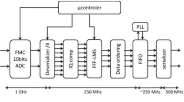
Digital Signal Processing
The Digital Signal Processing implemented in this paper is presented Fig.1.
The received analogue signal is sampled at 1 GSps by a pair of 10 bits resolution ADC, giving In-phase(I) and Quadrature phase(Q) digital signals. Both of them are then de-serialized to match the FPGA clock at 250MHz. An IQ compensator corrects the unbalanced default from optical and RF sub-system. An eleven taps T/2-fractionaly spaced adaptive equalizer, based on Least Mean Square (LMS) error, is used to compensate the channel intersymbol interference and the carrier frequency offset. Due to the sampling rate higher than the FPGA processing frequency, algorithms are computed by a full pipelined parallel architecture. Thereby, two processing units compute input data. This architecture is easily scalable for higher sampling rate frequency ratio. Two T/2-adaptive equalizers compute two consecutives symbols. The coefficients are identical for both filters and are updated at each FPGA cycle for maximal sampling and carrier frequency offset tolerance. Instead of classic solutions combining Gardner[5],[6] and a frequency recovery loop for the sampling frequency offset (SFO) compensation, a smart implementable solution using center-tap tracking algorithm[4] is implemented. This algorithm analyses the filters coefficients magnitudes and operates a
Fig. 1: Digital Signal Processing (FFF:
coefficient shift to keep the maximum energy on the central coefficient. If the TX sampling frequency is greater than the RX one, coefficients are shifted to the left and an additional symbol has to be computed compensating the temporal output shift. This is done through a dedicated third filter. Reciprocally, in the case of right shift, a redundant symbol is removed from the output stream.
Due to irregular data flow at the output of the decisions blocks, data are memorized in a First In First Out (FIFO) buffer. An FPGA internal Phase Locked Loop (PLL), controlled by FIFO filling, creates an image of the TX clock.
Boards used are FMC126 (FPGA Mezzanine Card) from 4DSP for the ADCs, VC707 from Xilinx for FPGA and HMC821 from Hittite for the sampling clock.
Tab. 1 highlights implementation results showing main FPGA resources usage. Although this study was performance oriented, it’s noticeable that few DSP resources (multipliers) are used.
Tab. 1: Ressources usage for Filter+LMS+ SFO+ décision
Resource Number of resources
DSP 143
Flip Flop 9484
LUT 5526
As described in Fig. 1, we propose a simple non-data aided (or unsupervised) transmission system because of its implementation efficiency and its ability to be scalable for higher sampling rates. We can notice that FMC126 supports 2GSps hence the proposed system can be easily upgraded for operating at 2GSps while keeping the same hardware configuration.
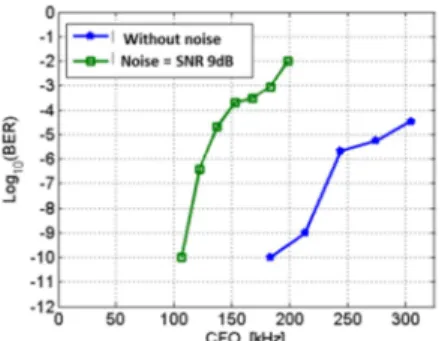
After processing by FPGA, the I/Q signals are analysed by a BER tester. The 1Gbitps QPSK signal used for measurement is generated with an 8GSps Arbitrary Waveform Generator (AWG). In first step, we have tested the
tolerance of our receiver to Carrier Frequency Offset (CFO) which is numerically generated and played by AWG. On Fig. 2, the CFO tolerance is greater than 100kHz with 9dB of SNR and 180kHZ without noise at error free.
System assessment
Our experimental set-up, equivalent to the one presented in[7],[8] is representative of a fully loaded 64 split class B+ PON.
The test RF signal is produced by the set of two AWG. The first AWG has two outputs with 1GSps, generating the QPSK baseband data with 500Mbps each and feeding the input of an IQ mixer. The RF Local Oscillator is obtained from a Frequency Synthesiser and can be tuned from 2 to 18GHz. The signal outputting the IQ mixer is called the “user signal” and is the one over which we measure the BER. The second AWG has 24GS/s capability and generates 11 dummy neighbouring RF channels around the users signal in order to simulate the presence of other users. This “complementary” signal occupies a bandwidth from 2 to 12GHz at maximum. A guard band of 20MHz is maintained each side of the user signal. The light is then amplified by an Erbium Doped Fibre Amplifier (EDFA) for an optical output power of +12dBm. To simulate a Passive Optical Network (PON) we use Standard Single Mode Fibre (SMF) spool (25 km long) and a Variable Optical Attenuator (VOA). A polarization scrambler is also used to make the set-up more realistic. Finally the light is photo-detected by a PIN photodiode with 7 GHz bandwidth and a responsivity of 0.8 A/W followed by a TIA. Then the signal inputs the receiver IQ mixer and ADC/FPGA board. The resulting BER is measured directly from the FPGA.
US Set-up (Fig. 4): An ECL is used to serve as LO in a coherent receiver and seed source for the reflective FDMA ONU. The launch power into the PON is set to +12dBm. The PON itself is made of a polarization scrambler followed by a 3dB optical coupler. After the coupler, two branches are considered. The first branch is made of a VOA, a 25km spool of SMF and reaches ONU1 whose structure is similar to the one reported in reference document[8]. Using the VOA, we can simulate optical budgets ranging from 16dB to over 40dB as required. The
Fig. 3: DS experimental set-up Fig. 2: B2B electric, error rate with phase rotation
second branch of the PON is made of another
3dB optical coupler. One branch is connected to a second ONU (denoted ONUx) while the other is connected to an EDFA used as Amplified Spontaneous Emission (ASE) source used to load the system with optical noise equivalent to the presence of 64 active ONUs on the PON
tree. ONU1 is modulated with a single user signal while ONUx is modulated with the complementary signal. At the OLT side, two RF signals are obtained from the coherent receiver as it is single polarization[7]. These signals are combined to produce another two signals containing the baseband data for the user signal under test[10] which can be used to feed directly the two 1GS/s ADC and FPGA where the BER is measured.
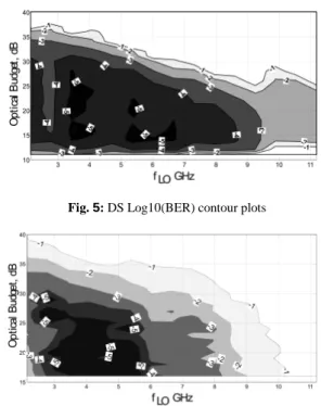
Results
Results are displayed in Fig. and Fig. . In the DS, it is possible to obtain a BER<10-3 up to 34dB of OB for the lowest frequency channel. Also, a BER of 10-3 could be obtained up to the channel whose centre frequency is 9GHz. In the US, an OB of 34dB is also demonstrated for the
lowest frequency channel for BER<10-3 while the last channel for which we can obtain a BER<10-3 is at 8GHz. Note that the limitations observed in these experiments rather come from the RF IQ mixers used and the roll-off of the frequency responses of the photodetectors and amplifiers rather than from the FDM receiver itself which operates purely in base-band.
Conclusions
For the first time, we have demonstrated in real-time the feasibility of a FDMA PON receiver at 1 Gbit/s for access network. We have developed transceiver modules for next generation PON systems that achieve smart implementable solution of the main digital signal processing functions.
Acknowledgements
This work has been carried out within the framework of the FAON project which is partly funded by the Agence Nationale de la Recherche under reference 11-INFR-005-01.
References
[1] L. Yuanqiu et al., “Time- and Wavelength-Division Multiplexed Passive Optical Network (TWDM-PON) for Next-Generation PON Stage 2 (NG-PON2),” JLT 31(4), p. 587-593, 2013
[2] G.989.1 : 40-Gigabit-capable passive optical networks (NG-PON2): General requirements
[3] C. Hungkei et al., “Demonstration of low-power bit-interleaving TDM PON,” ECOC, Paper Mo.2.B.1, 2012 [4] R. Gitlin et al. “Center-tap tracking algorithms for timing
recovery” AT&T Technical Journal Vol.66 Issue.6 Part.2, 1987
[5] Gardner, F.M., A BPSK/QPSK timing error detector for
sampled receivers. IEEE Transactions on
Communications, vol.34, pp.423–429, 1986
[6] R. M. Ferreira et al, Impact of TWDM on Optional Real-Time QPSK WDM Channels, ECOC 2014, P.7.19 [7] S. Straullu et al., “Single-Wavelength Downstream
FDMA-PON at 32 Gbps and 34 dB ODN Loss,” PTL 27(7), p. 774 - 777 F. (2015).
[8] S. Straullu et al., “Optimization of Reflective FDMA-PON Architecture to Achieve 32 Gb/s Per Upstream Wavelength Over 31 dB ODN Loss,” JLT 33(2), p. 474 – 480 (2015).
[9] B. Charbonnier et al, “Silicon photonics for next generation FDM/FDMA PON,” JOCN 4(9), p. A29-37, (2012).
[10] B. Charbonnier et al., “Demonstration of low DSP requirements for FDMA PON,” ECOC, P.7.5 (2014). Fig. 4: US experimental set-up
Fig. 5: DS Log10(BER) contour plots