HAL Id: cea-01842332
https://hal-cea.archives-ouvertes.fr/cea-01842332
Submitted on 15 Jan 2019
HAL is a multi-disciplinary open access
archive for the deposit and dissemination of
sci-entific research documents, whether they are
pub-lished or not. The documents may come from
teaching and research institutions in France or
abroad, or from public or private research centers.
L’archive ouverte pluridisciplinaire HAL, est
destinée au dépôt et à la diffusion de documents
scientifiques de niveau recherche, publiés ou non,
émanant des établissements d’enseignement et de
recherche français ou étrangers, des laboratoires
publics ou privés.
Diamond micro-electrode arrays (MEAs): A new route
for in-vitro applications
Myline Cottance, Sebastien Nazeer, Rousseau Lionel, Gaelle Lissorgues,
Alexandre Bongrain, Raphael Kiran, Emmanuel Scorsone, Philippe Bergonzo,
Amel Bendali, Serge Picaud, et al.
To cite this version:
Myline Cottance, Sebastien Nazeer, Rousseau Lionel, Gaelle Lissorgues, Alexandre Bongrain, et al..
Diamond micro-electrode arrays (MEAs): A new route for in-vitro applications. 2013 Symposium on
Design, Test, Integration and Packaging of MEMS/MOEMS (DTIP), Apr 2013, Barcelona, Spain.
�cea-01842332�
Diamond Micro-Electrode Arrays (MEAs): a new
route for in-vitro applications.
Myline Cottance
1, Sébastien Nazeer
1, Lionel Rousseau
1, Gaëlle Lissorgues
1, Alexandre Bongrain
2,
Raphaël Kiran
2, Emmanuel Scorsone
2, Philippe Bergonzo
2, Amel Bendali
3, Serge Picaud
3, Sébastien Joucla
4,
Blaise Yvert
41 Université Paris-Est, ESYCOM, ESIEE Paris (Engineering School), 2 boulevard Blaise Pascal, 93162 Noisy le Grand, France
E-mail :[email protected], [email protected],[email protected],[email protected] 2 CEA LIST, Diamond Sensors Laboratory, F-91191 Gif-sur-Yvette, France
E-mail : [email protected]
,
[email protected],[email protected],[email protected]3 Institut de la Vision, UMRS 968 Inserm/UPMC, UMR7210 CNRS, 17 Rue Moreau, 75012 Paris, France
E-mail :[email protected], [email protected]
4 CNRS and Université de Bordeaux, INCIA, Bât B2, Avenue des Facultés, 33405 Talence, France.
E-mail : [email protected],[email protected]
Abstract- Microelectrode arrays (MEAs) are extracellular devices allowing both recording and electrical stimulation of neuronal or cardiac cells. Interfacing cellular networks with MEAs leads to a better knowledge and understanding of the mechanisms of biological tissue and can be used for restorative purposes using neural prosthesis. We report the fabrication of in vitro 8×8 and 4×15 planar boron-doped nanocrystalline diamond (BNCD) MEAs using microtechnology. The BNCD for our MEA electrodes have been characterized electrochemically and we show that these devices offer good recording properties as compared to other standard electrode materials (such as Ti-Pt or Au).
Index Terms- microelectrode arrays, electrical stimulation, recording, neural network, diamond electrode.
I. INTRODUCTION
Micro-Electrode Arrays (MEAs) were developed since the early 1970s and play an important role in the comprehension of the mechanisms of electrogenic cell biological activity. They are widely used in various domains especially in neuroscience as they correspond to non-invasive techniques that allow both long-term stimulation and recording of bio-electrical signals of cultured cells and tissues [1]. For instance, MEAs can help to understand some currently misunderstood phenomena such as extracellular electrical stimulation mechanisms that excite nervous cells. In clinical research, extracellular electrical stimulation of the central nervous system is used in therapeutic aims to restore different sensory or motor functions (retinal [2] and cochlear implants [3], lesioned spinal cord stimulation [4], deep brain stimulation [5]). In fundamental research, this type of stimulation is used as a tool to investigate network of neurons to highlight their organization, connectivity, and also to study their modification in response to external stimulation. MEAs also enable extracellular electrical recordings which allow gaining of information about interactions between electrogenic cells, sampling distribution of electrophysiological behavior and/or monitoring changes of
electrical activity which are suitable for drug screening and discovery applications [6].
Here, we report on the fabrication of diamond planar MEAs of two matrix geometries, 8×8 and 4×15, designed for the stimulation and recording of respectively rat retina and mouse embryonic spinal cord. The material electrode chosen in this study is the boron-doped nanocrystalline diamond (BNCD) as it exhibits many valued advantages due to its physical and chemical properties [7] compared with common platinum and gold electrodes. Besides its 3V electrochemical water potential, BNCD also display biocompatible properties which render this material ideal for biological in-vitro applications. Moreover, the novelty of the work is related to an original process development since diamond growth is not obviously compatible with standard silicon micro-fabrication steps due to temperature constraints.
II. METHODS
A. Designs of MEAs
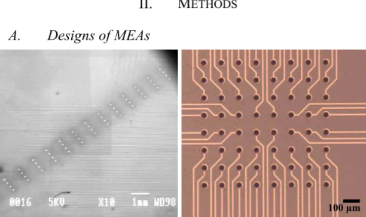
Fig. 1. On the left, electrodes arranged in a 4×15 matrix and on the right electrodes arranged in an 8×8 matrix.
Two designs of MEAs depicted in Fig. 1, were fabricated in order to suit the geometry of studied tissues for a better recording and stimulation of cells.
The first design consists of circular electrodes of 80 µm
diameter of unique size and 300×900 µm pitch arranged in a 4×15 matrix. It is adapted to the geometry of mouse embryonic hindbrain-spinal cord preparation with an active area of 11.34 mm².
The second design is made of circular electrodes of 34 µm diameter of unique size and 100 µm pitch arranged in an 8×8 matrix and it is adapted to the geometry of rat retina preparation with an active area of 0.49 mm².
B. Fabrication process of MEAs
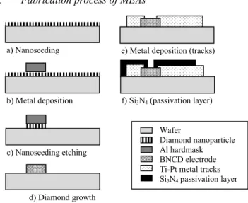
Fig. 2. Process flow of diamond MEAs fabrication process
We have investigated previously a process where we deposited the metal layer for contacting the diamond before growing diamond on top of the metal. Because of high temperature required for the diamond growth (above 850°C), the metal exhibits a blistered and cracked surface resulting in poor adhesion to the substrate. As the steps order was mainly governed by diamond growth temperature, a new fabrication process of diamond MEAs is developed (Fig. 2) where diamond is grown before metal deposition. First, detonation diamond nanoparticles were spin coated on a 4 inches silicon or glass wafer using the process described in [8]. An aluminum hard mask was then sputter deposited to define electrode shape by lithography. Diamond nanoparticles outside these protected areas were etched away using a short oxygen reactive ion etch (RIE) plasma. Next, the metal hard mask was removed chemically to reveal the diamond particles patterns which thus were exposed to a gas mixture of methane, hydrogen and trimethylboron in a MPECVD (Microwave Plasma Enhanced Chemical Vapor Deposition) diamond growth reactor (Seki technotron corp. AX6500X). The grown electrodes were individually contacted by the sputtered deposition of Ti (50 nm)/ Pt (150 nm) metal tracks using the lift-off process and Nlof 2020 as a sacrificial photoresist layer. A 600 nm silicon nitride (Si3N4) layer was deposited
on the substrate by plasma-enhanced chemical vapor deposition in order to insulate the metal tracks from the electrolyte solution. Then, a sulfur hexafluoride (SF6) RIE
was performed to etch locally the silicon nitride to open contact pads and diamond electrodes, which also defines the electrode size. Finally, the photoresist used to selectively
etch the nitride layer was removed and the MEAs were diced using a diamond saw, being ready to be used for biology.
III. RESULTS
A. Morphological characterization
Fig. 3. Optical microscope images of a 80 µm diamond electrode of a 4×15 MEA before passivation (on the left), and a 34 µm diamond electrode of a
8×8 MEA after passivation (on the right).
The grown diamond electrodes, characterized using a UV–Vis Spectroscopic Ellipsometer (Horiba Jobin- Yvon, UVISEL), present a thickness of approximately 300 nm over a diameter of 80 µm for the 4×15 MEA. After the passivation step which defines the active area, electrodes exhibit a smooth surface aspect and metal annular contacts and tracks are well defined as shown in Fig. 3.
Fig. 4. SEM image of BNCD film
The morphology and grain size were observed using scanning electron microscopy (SEM). The typical morphology of a boron-doped diamond layer is shown in Fig. 4. The diamond crystals are highly faceted, with an average grain size of 100 nm and the obtained diamond films are uniform and continuous. The measured boron concentration determined with a secondary ion mass spectrometry (SIMS) depth profiling using a Cameca IMS 4f ion microprobe was approximately 2×10²¹ at.cm−3.
B. Electrochemical characterization
Cyclic voltammetry (CV) provides information on the potential window of the electrode which is the voltage range between which the material electrode does not induce water oxidation nor reduction. This window is important for the stability of cells and tissues facing the electrodes to prevent them to be exposed to ionic species nor hostile pH.
Fig. 5 presents the result of CV characteristics as probed on our manufactured diamond MEA electrode (80-µm diameter) in a 0.5 M aqueous LiClO4 solution scanned at
20 µm 50 µm d) Diamond growth Wafer Diamond nanoparticle Al hardmask BNCD electrode Ti-Pt metal tracks Si3N4 passivation layer a) Nanoseeding
b) Metal deposition
c) Nanoseeding etching
e) Metal deposition (tracks)
0.1 V.s-1. This experiment demonstrates that diamond
electrodes have a wider window potential (3.5 V) than platinum and gold electrodes (2.5 V) reported in literature [9, 10].
Fig. 6 presents the CV of the same electrode in a ferri/ferrocyanide solution where the peak to peak separation of the oxidation and reduction potential was probed at 63 mV at a 0.1 V.s-1 scan rate. This experiment
demonstrates the extreme reactivity of the diamond surface. This wide potential window of diamond can be explained by the inertness of its surface for adsorption (hydrogen termination) [11].
Fig. 5. CV of diamond electrodes on a 0.5 M aqueous LiClO4 solution scanned at 0.1 V.s-1.
Fig. 6. CV of diamond electrodes in ferri/ferrocyanide scanned at 0.1 V s-1.
Electrochemical impedance spectroscopy (EIS) was also performed to study the impedance of the electrode. Measurements were made at 1 kHz (sine wave) thus corresponding to characteristic frequency of neural biological activity. They are performed using a NanoZ device (Fig. 7) from Multichannel Systems (Reutlingen, Germany) with an Ag/AgCl electrode in phosphate buffered saline (PBS) aqueous solution of pH 7.2. The equipment gives the magnitude and phase of the impedance value for each electrode.
We found at 1 kHz that impedance values were within
200-300 kΩ for 80-µm planar electrodes.
Fig. 7. A 8×8 MEA fixed on NanoZ device to measure the magnitude and phase of the electrode impedance at 1 kHz.
C. Functional Tests
Two sets of experiments are currently being performed with the fabricated MEAs: the first one is the extracellular signal recording and electrical stimulation of an embryonic mouse hindbrain-spinal cord and the second one is the recording of spontaneous extracellular signals of a retina.
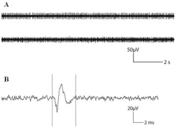
Preliminary results obtained on a whole embryonic hindbrain-spinal cord (as in [12]) show that BNCD MEAs could successfully detect spontaneous activity composed of spike bursts with and amplitude in the range of a few µV and lasting for a few seconds (see Fig. 8).
Fig. 8. Recording of a spike burst with a 4×15 matrix diamond MEA.
Extracellular recordings of spontaneous activity of an ex
vivo rat retina on an 8×8 MEA are shown in Fig. 8. Pieces
of retina were placed on the array with the ganglion cells (spiking neurons in the retina) facing the electrodes. Spontaneous activities of a retina were recorded on several electrodes of which two recordings of two different electrodes can be seen on Fig. 9 (A) and an enlargement of the recording exhibits on Fig. 9 (B), a typical shape of a recorded action potential.
C u rrent d ens it y (µ A/c m ²) Potential (V) Electrochemical window of Diamond : 3.5 V C u rrent d ens it y (µ A/c m ²) Potential (V vs. Ag/AgCl)
Fig. 9. Spontaneous activity of a retina recorded with a 8×8 matrix diamond MEA: (A) trace recorded during 10s, (B) typical shape of a
recorded action potential.
IV. CONCLUSION
We have presented a novel microfabrication process of diamond planar MEAs, assessing that the combination of standard silicon micro-fabrication processes with diamond growth is possible to fabricate functional devices for neural recordings.
The manufactured MEAs were characterized with cyclic voltammetry demonstrating that MEAs were successfully fabricated. The wider potential window of diamond compared to other material electrode is an important attractive feature for sensor applications [10].
In-vitro electrical recordings of spontaneous activity of an embryonic mouse hindbrain-spinal cord with our 4×15 MEA and of a retina rat with our fabricated 8×8 MEA were successfully accomplished. Extracellular electrical neural stimulation using MEAs is the purpose of current development.
New materials or combination of materials will be also studied to improve our MEAs properties. Moreover, as our MEAs and diamond material exhibit promising results, they also led us to head towards in-vivo applications such as working on the development of retinal implants with similar diamond electrodes.
ACKNOWLEDGMENT
The authors would like to thank the French National Research Agency for their financial support through the MEDINAS project as well as the European Community's Seventh Framework Programme (FP7) under grant agreement n° 280433 (NEUROCARE project).
REFERENCES
[1] F. O. Morin, Y. Tkamura, E. Tamiya, “Investigating Neural Activity with Planar Microelectrode Arrays: Achievements and New Perspectives”, vol. 100, N°2, pp. 131-143, 2005.
[2] J.-U. Meyer, “Retina implant – a bioMEMS challenge”, Sensors
and Actuators. A, Physical A 97-98, pp. 1-9, 2002
[3] B. S. Wilson and M. F. Dorman, “Cochlear implants: Current designs and future possibilities,” JRRD, Vol. 45, N° 5, pp. 695-730, 2008.
[4] T. S. Grabow and al., “Spinal Cord Stimulation for Complex Regional Pain Syndrome: An evidence-based Medicine Review of the literature,” The Clinical Journal of Pain, Vol. 19, No. 6, pp. 371-383, 2003.
[5] V. Voon and al., “Deep Brain Stimulation: Neuropsychological and Neuropsychiatric Issues”, Movement Disorders, Vol. 21,
Suppl. 14, pp. 305-326, 2006.
[6] A. Stett and al., “Biological application of microelectrode arrays in drug discovery and basic research”, Anal Bioanal Chem, vol. 377, pp. 486-495, 2003.
[7] A. Fraft, “Doped Diamond: A Compact Review on a New, Versatile Electrode Material”, Int. J. Electrochem. Sci., Vol. 2, pp.
355-385, 2007.
[8] E. Scorsone, S. Saada, J.C. Arnault, P. Bergonzo, “Enhanced control of diamond nanoparticle seeding using a polymer matrix,”
J. Appl. Phys., vol. 106, 014908, 2009.
[9] A. Kraft, “Doped Diamond: A Compact Review on a New , Versatile Electrode Material”. Int. J. Electrochem. Sci., Vol. 2, 355-385, 2007.
[10] C. E. Nebel and al., “Diamond for bio-sensor applications”,
Journal of Physics D: Applied Physics, 40(20), 6443–6466, 2007.
[11] M. Alexander, M. N. Latto, G. Pastor-Moreno, D. J. Riley, The influence of surface termination on the electrochemical properties of boron doped diamond, Electrochem Soc. Proceedings, Vol. 2001-25, 2001.
[12] B. Yvert, C. Mazzocco, S. Joucla, A. Langla, P. Meyrand, “Artificial CSF motion ensures rhythmic activity in the developing CNS ex vivo : A mechanical source of rhythmogenesis?”, Journal
of Neuroscience, 31:8832-8840, 2011.
BIOGRAPHY
Myline Cottance got her bachelor's degree in organic chemistry in 2010 from the Science Faculty of Orsay and her master's degree in chemical engineering in 2011 from the University of Pierre and Marie Curie. She currently conducts PhD studies at ESIEE-Paris working on the fabrication of MEAs for retinal implants and neuro-electronic interfaces.