HAL Id: in2p3-00161376
http://hal.in2p3.fr/in2p3-00161376
Submitted on 10 Jul 2007
HAL is a multi-disciplinary open access
archive for the deposit and dissemination of
sci-entific research documents, whether they are
pub-lished or not. The documents may come from
teaching and research institutions in France or
abroad, or from public or private research centers.
L’archive ouverte pluridisciplinaire HAL, est
destinée au dépôt et à la diffusion de documents
scientifiques de niveau recherche, publiés ou non,
émanant des établissements d’enseignement et de
recherche français ou étrangers, des laboratoires
publics ou privés.
A Low Power Multi-Channel Single Ramp ADC With
up to 3.2 GHz Virtual Clock
E. Delagnes, D. Breton, F. Lugiez, R. Rahmanifard
To cite this version:
E. Delagnes, D. Breton, F. Lugiez, R. Rahmanifard. A Low Power Multi-Channel Single Ramp
ADC With up to 3.2 GHz Virtual Clock. 2006 IEEE Nuclear Science Symposium, Medical Imaging
Conference, and 15th International Room Temperature Semiconductor Detector Workshop, Oct 2006,
San Diego, United States. �in2p3-00161376�
Eric Delagnes, Dominique Breton, Francis Lugiez, and Reza Rahmanifard
Abstract– During the last decade, ADCs using single ramp
architecture have been widely used in integrated circuits dedicated to nuclear science applications. These types of converters are actually very well suited for low power, multi-channel applications. Moreover their wide dynamic range and their very good differential non-linearity are perfectly matched to spectroscopy measurement. Unfortunately, their use is limited by their long conversion time, itself limited by their maximum clock frequency. A new architecture is described in this paper. It permits speeding up the conversion time of the traditional ramp ADC structures by a factor of 32 while keeping a low power consumption. Measurement results on a 4-channel, 12-bit prototype using a 3.2 GHz virtual clock are then presented in detail, showing excellent performances of linearity and noise.
Index Terms– Analog-digital conversion, Time measurement,
Delay lock loop, Mixed analog-digital integrated circuits, Front-end electronics, CMOS.
I. INTRODUCTION
HE trend in data acquisition systems for modern physics experiments is to digitize signals closer and closer to the detector. With the very high level of integration achievable with modern submicron technologies, the benefit of integrating inside the same chip the analog front-end, the digitization, and a part of the digital treatment is becoming more and more obvious. Nevertheless, the design of high performances ADCs remains a difficult task. As the nuclear science detector granularity is continuously increasing, and thus the number of channels, the readout circuits are becoming massively multi-channel. For these two reasons, multi-channel integrated ADCs are becoming necessary. Multi-channel lower speed ADCs, associated with demultiplexing structures based on fast analog memories, may also replace a high speed ADC.
Today, a large spectrum of ADC architectures is available. But, for applications with a large number of channels and a dynamic range higher than 6 bits, flash architecture are excluded by power dissipation and area constraints. Semi-flash or pipelined architecture, at the basis of most of the modern commercial ADCs, are better suited. But they are more difficult to design, especially if good
Manuscript received March 12, 2007.
E. Delagnes and F. Lugiez are with CEA, DSM/DAPNIA, CE-Saclay, F-91191 Gif-sur-Yvette Cedex, France (email: eric.delagnes@cea.fr).
D. Breton is with CNRS/LAL, BP34, 91898 Orsay, France.
R. Rahmanifard was with CEA/DSM/DAPNIA during the chip design, he is now with, L.E.A. Immeuble Lafayette 2 Place des Vosges 92051 Paris La Défense , France
differential linearity performances are required. Successive approximation architectures are easier to design, but their area may become prohibitive if a large dynamic range and a good linearity are needed.
II. THE SINGLE RAMP ADCARCHITECTURE AND ITS LIMITATIONS
At last, the single ramp architecture appears to be the easier to design and the most adapted to multi-channel circuits. It has been widely used in front-end ASIC [1] for two decades. Several types of implementations of this architecture are possible. In the most efficient one, the voltage to digital conversion is performed by measuring the time between the start of a voltage ramp and its crossing, detected by the comparator, of the voltage to be converted. Classically, the time measurement is achieved by a counter started synchronously with the ramp as shown on Fig. 1. To avoid metastability effects, a resynchronization of the comparator output by the clock of the counter is required to stop or memorize the counter state.
Fig. 1. Chronogram of the standard single ramp ADC operation.
The main advantage of this particular implementation is that , as appearing on Fig. 2, the counter and the ramp generator can be shared between the channels so that the ADC part replicated in each channel can be reduced to a discriminator and a memory used to copy and memorize the counter state when the discriminator triggers. So the power consumption and the area used can be very small even for high dynamic range and the linearity, mainly dominated by that of the ramp generator, can easily be very good. But, unfortunately, the use
A Low Power Multi-Channel Single Ramp ADC
With up to 3.2 GHz Virtual Clock
of this kind of ADC is limited by its long conversion time. In fact, for an N bit conversion, it requires 2N / Fck, where Fck is the clock period of the counter. So for a 12-bit conversion, making use of a 100 MHz clock, which appears to be a maximum for reasonable power consumption, 40 µs are required. This time is prohibitive for a lot of applications.
Fig. 2. Possible architecture for a standard multi-channel single ramp-ADC.
III. ANEW ARCHITECTURE TO SPEED UP SINGLE RAMP ADCS
A. Global Architecture and main choices.
In the new architecture, as in the usual one, the analog to digital conversion is performed by a time measurement, but with a better time resolution. To achieve this, we propose to virtually increase the counter clock frequency. For this purpose, a structure similar to those of modern Time to Digital Converters, also used in the field of High Energy Physics instrumentation [2,3], will be used to measure the ramping time. As in modern TDC, the most significant bits of the conversion are obtained by a counter operating at moderate Fck frequency while the least significant bits are obtained thanks the use of a Delay Lock Loop (DLL). Many different implementations of this principle are possible, we have chosen one based on the Nutt method also used in [2].
As in the previous designs, the counter and the ramp are started simultaneously. When a comparator triggers, its output is synchronized by the clock to memorize the state of the counter. In parallel the asynchronous signal output of the comparator is sent to the input of the DLL. Then the DLL is frozen by the resynchronized comparator signal, so that the DLL memorized state is a measurement, with a 1/(m.Fck)
precision, of the elapsed time between the triggering of the comparator and the next clock edge used to memorize the state of the counter.
The main interest of this architecture is, for a given clock frequency, to decrease by a factor m the time required for the conversion and this without any power consumption penalty.
B. Main specifications for a demonstrator chip.
To validate this architecture a 4-channel demonstrator, named WILKY, has been designed in the AMS CMOS 0.35µm technology. Its specifications were defined to match those of the SAM chip [4] for the H.E.S.S.-II experiment:
- 12-bit dynamic range (and precision) over a 2 V full range: LSB value of 0.5 mV
- Power consumption < 1 mW per channel - Easily extendable up to 64 channels.
- For this design, nominal values of Fck = 100 MHz and m = 32 have been chosen. Thus the LSB time step is 312.5 ps and the maximum conversion time is 1.3 µs. It corresponds to a virtual frequency of 3.2 GHz.
- Reasonable stability with temperature.
This implies that in the WILKY chip the seven most significant bits will be obtained from the counter whereas the five less significant ones will come from the DLL.
IV. DETAILED DESIGN DESCRIPTION.
A. The Counter.
As in the previous designs [1], the counter is using gray code. In this code, only one bit is changing between two consecutive codes. This minimizes the digital noise and decrease the power consumption of both the counter itself and the digital buffers needed to drive the counter outputs through the channels. This counter is based on a cascade of elementary modular asynchronous blocks.
Its depth is programmable from 6 to 10 bits with a nominal value of 7 bits.
B. The Synchronizer.
To deal with metastability effects, the block resynchronising the discriminator output is using two cascaded RS latch. The first one has its clock input connected to the clock, the second one uses the clock delayed by four cascaded elementary delays similar to those used in the DLL and using the same control voltage. This design minimizes the delay induced by the synchronizer.
C. The DLL.
As shown on Fig. 4, the total propagation time of the DLL must be larger than the clock period to compensate for the latency of the synchronizer and to deal with edges effects and unexpected delays in the design. For this purpose, m+p elementary delays, of 1/(m.Fck) each, are
used. In the WILKY prototype the value m=32 and p=8 have been chosen. The DLL elementary delay is the cascade of two starved inverters. The DLL states are memorized by RS latches, more compact than DFF, when the resynchronized comparator output is triggered.
The main advantage of this architecture including a DLL in each channel is that digital signals are propagating in the DLL only after the comparison is achieved. It minimizes digital activities and so power consumption and noise compared to alternative designs with master DLL continuously operating with the clock [2].
But it requires special calibration phases during which the total delay of each DLL must be servo-controlled to (m+p)/(m . Fck). To perform this operation, a calibration pulse is sent to the input of the DLL. The phase of the DLL output is compared with the one of the calibration pulse delayed by one clock period (by a DFF) plus p elementary delays.
The output of the phase comparator drives a charge pump providing the voltage controlling the elementary delay value. A minimum of two clock periods are required for this calibration phase, adding extra dead time in the conversion. Practically, at the “cold start” of the ADC operation, 70 calibration pulses are required to ensure the DLL convergence. Afterward, a 50µs calibration periodicity is enough to compensate the charge pump leakages. In the nominal operation, with a 700 kHz repetitive conversion rate, a 2-clock duration calibration phase only is performed at the beginning of each conversion.
D. The ramp generator.
The fast conversion implies a larger sensitivity to the timing parameters of the ramp generator. Both the slope and the offsets of the ramp must be stable with temperature. To achieve a good linearity, the ramp generator, shown on Fig. 5, is based on the integration of a constant current by an active integrator.
Fig. 5. Principle of the common ramp generator.
To ensure the required stability with temperature: - The current source is servo-controlled.
- All the injected charges are minimized or cancelled by use of dummy switches.
- The differential input pair of the integrator operational amplifier is biased with a transconductance stable with temperature, in order to ensure a constant gain-bandwidth product of the OPAMP.
The rms noise of the voltage ramp scales with the time as: Vn = 1/Ci .( A . t + B . t2 )1/2 (1)
where Ci is the integration capacitor and A and B coefficients related to respectively the thermal and 1/f contribution to the noise of the current source.
For a given ramp noise, a faster conversion, like that possible with this design makes it possible to decrease the value of the integration capacitor and then to decrease the size of the ADC. In this design the value of this capacitor is only 5 pF.
E. The comparator.
The fast conversion makes this block really critical. Its delay must be very stable with both the input level and temperature variations. To achieve this, a first solution would be to use a very fast comparator. This solution was eliminated because of its huge power consumption, incompatible with the replication of the comparator in each channel. Instead, a moderate speed, low power structure has been chosen. As shown on Fig. 6, the comparator is based on the cascade of three moderate gain stages followed by a digital level restorer. Actually, this structure is the one offering the best speed-power trade-off.
Fig. 6. Principle of the comparator.
The three *10 gain stages of Fig. 7 (right side), are based on simple differential stages. A cascod pair is used to increase speed and to decrease sensitivity to the input level. These gain stages are biased with a temperature-stabilized current source. The active loads of these stages consist of a PMOS used as a diode in parallel with a second PMOS used as a voltage-controlled resistor. This load behaves like a resistor for small signals and limits the output swing for larger signals. The active resistor value is controlled by the voltage reference common to all the channels of Fig. 7 (left side). This reference uses a replica of the active load to servo-control the gate voltage of the PMOS resistor in order to set the quiescent output voltage of the gain stage and therefore the resistance of the active load.
Fig. 7. Replica-based voltage reference (left side) and Gain stage (right stage) used in the comparator.
The carefully control of the output swings and output resistances ensure a good stability of their delays.
F. Maximum conversion rate.
The practical conversion time is (6 + 2 Nc )/ Fck where Nc is the number of bits obtained with the counter. The 6 extra clock periods are needed for the following reasons: - 2 for DLL calibration before conversion
- 2 after the ramp start to wait for the ramp to enter its very linear region.
- 1 for the comparator output synchronization. - 1 for DLL encoding.
For a 100 MHz clock Frequency, the conversion time is then 1.34 µS, corresponding to a 746 kHz maximum rate.
V. PERFORMANCES OF THE PROTOTYPE CHIP. The 4-channel WILKY prototype is very compact. The area of the common ramp and counter block is 300 µm x 300 µm whereas 1 mm x 34 µm are needed for each channel. The form factor has been optimized for a multichannel application.
On this prototype, the depth of the counter together with the slope and the offset of the ramp are tunable in order to explore several possible operation modes of the ADC.
The ADC prototype has been tested using a USB test bench based on a 16-bit 4-channel DAC with a 75 µV LSB. The DAC channels are used as quasi-static inputs for the ADC prototype.
A. Test in the Standard Mode.
The prototype has been firstly tested in his nominal configuration: 12-bit dynamic range, 100 MHz clock. In this configuration, with a power supply voltage of 3.3 V, the power consumption is only of 3.3 mW + 0.5mW/channel.
Fig. 8. ADC transfer function in standard mode (data and linear fit superimposed).
The ADC LSB, calculated from the transfer of Fig.8 function is 534 µV. It can be noticed that the range of the ADC is actually larger than 2V, and that the code delivered by the ADC can be larger than 4096 because the maximum counter depth was set to 8 bits.
Fig. 9. Integral Non Linearity as a function of ADC output code.
The Integral Non Linearity (INL) plotted on Fig. 9 shows the residue to a linear fit performed on the data of Fig. 8. The INL is less than +/-1 LSB over the 12-bit range. A zoom of the INL, shown on Fig. 10, reveals a periodicity of 32 ADC counts in the INL characteristic.
For each input voltage of the Fig.8 transfer function, 512 acquisitions have been performed and standard deviations on these measurements have been calculated. They are plotted on Fig. 11 as a function of the mean ADC code obtained. The noise is smaller than 0.6 LSB and is increasing with the ADC code as expected from the theoretical noise behavior of the voltage ramp. As for INL, the noise characteristic also reveals a 32 ADC-count periodicity.
The ADC Differential Non-Linearity (DNL) has been characterized using the statistical density of code method assuming a good enough linearity of the test DAC. On Fig.
12, the normalized density of code is plotted as a function of the ADC code. It is equivalent to 1 + DNL.
Fig. 10. Zoom on the Fig. 10 plot.
Fig. 11. Variation of noise with ADC output code.
Fig. 12. Normalized statistical density code as a function of ADC output code.
The DNL value is smaller than +/- 0.2 LSB peak to peak, or equivalent to 0.1 LSB rms. As for INL and noise, a zoom on the DNL characteristic reveals a pattern with a periodicity of 32. This pattern appears to be the major contributor to DNL.
Fig. 13. DLL codes probability density.
In Fig. 13, the statistical density of code method has been applied only to the 5 bits provided by the DLL. The characteristic is not flat: some codes are more probable than others. It means that the DLL is not perfectly linear. The DNL of the DLL can be estimated to +/- 0.15 LSB, corresponding in the time domain to +/- 50 ps peak to peak or 20 ps rms. This pattern is the main contributor to the ADC DNL and INL periodicity. It is similar on all the channels and is probably due to digital couplings inside the DLL.
The offset between channels is 15 mV peak to peak in good agreement with monte-carlo simulations. The spread of transfer function between channels is smaller than +/-1/1000, this is slightly larger than the expected value. No crosstalk between channels is measurable.
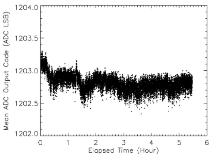
Fig. 14 demonstrates the good stability of the ADC measurement with time for a fixed input and Fig. 15 its low sensitivity to temperature variations.
Fig. 14. Stability of the ADC measurement with time. Each plotted dot is the mean value of 512 measurements.
Fig. 15. Variation of the ADC measurements with temperature. Each plotted dot is the mean value of 512 measurements.
The drift due to temperature is less than 3 LSB in a 10°C range. It is better than our expectation and sufficient for our applications. The shape of the temperature characteristic appears to be identical on all channels.
The performances of the ADC used in the standard mode are excellent and comparable to those of a genuine 12-bit ADC. If we consider that the prototype is a real 12-bit ADC we can calculate its Figure of Merit (FOM) defined in [5] by FOM = (P / (2NBits . 2 . FBW)) (2)
where FBW is the ADC Nyquist frequency - we will take equal to conversion frequency divided by 2 for the calculation - and P is the ADC power consumption.
The FOM is equal to 1.2 pJ/conversion in the case of a single channel ADC but is decreased to respectively 0.4 pJ/conv and 0.2 pJ/conv in the cases of a 4 or a 32-channel ADC as the power of the common block is shared between the channels. These FOM values are comparable to the one obtained on the best ADCs using deep-submicron technologies. This has to be temperate by the fact that there is no track and hold stage included in this architecture. B. Tests in other conditions.
The ADC has been also successfully tested with 25 and 50 MHz master clocks. In theses conditions the results are comparable to those obtained at 100 MHz with only a 10 to 20% noise increase for the largest codes due to the largest noise of the longer ramps as expected from (1).
A test has also been performed with a ramp slope decreased to obtain a larger LSB value of 1 mV, but over a dynamic range of only 8 bits. With Fck=100 MHz it means a 140 ns conversion time. The INL, measured in these conditions, is plotted in Fig. 15. It is smaller than +/-0.7 LSB, clearly dominated by the modulo-32 pattern. This is again due to the DLL non linearity contribution which remains unchanged in this case compared to the nominal one.
Fig. 16. ADC Integral Non Linearity as a function of ADC output code in the 8bit, 1mV LSB configuration.
The funny shape of the variance versus mean ADC code characteristic of Fig. 16, measured in this condition, is exactly the one due to quantization effects expected on a low noise ADC: the variance is 0 when the voltage is in the middle of the code and is reaching a maximum value of 0.5 when it is approaching the limit between two codes. A noise of 0.15 LSB rms corresponding to the ramp and the comparator noises have been computed from this characteristic.
Fig. 17. Zoom on the variance vs mean ADC measured in the 8-bit, 1mV LSB configuration.
The chip has also been characterized with a smallest LSB of 270 µV over a dynamic range of 13 bits corresponding to a longer conversion time of 2.6 µs.
In this configuration, the INL, plotted on Fig. 18 is smaller than +/- 3 LSB. The noise plotted in Fig. 19 is increasing from 0.7 to 1.2 LSB rms with the ADC code. This is corresponding to almost the same noise voltages than in the standard mode.
Fig. 18. ADC Integral Non Linearity as a function of ADC output code in the 13bit, 270µV LSB configuration.
Fig. 19. ADC noise as a function of ADC output code in the 13bit, 270µV LSB configuration.
For this reason this LSB value seems to be the smallest practicable. To decrease it, the noise of the ramp generator at large ramp voltages should be decreased by increasing the integrating capacitor of Fig. 5.
VI. CONCLUSION.
A new multi-channel single ramp ADC architecture has been proposed, prototyped and tested. It permits increasing the conversion speed by a factor of 32 without power consumption or other performances penalties. The characterization of the prototype in its nominal 12-bit/1.34µs configuration has shown excellent performances compatible with a real 12-bit operation together with a good stability. Its differential non-linearity performances make it usable for spectroscopy applications. Considering these excellent results, a 64-channel version of this ADC is going to be integrated on the next generation of a gigaHertz analog memory dedicated to the future Cherenkov Telescope Arrays [4].
Extra measurements, made on other configurations have shown that it is possible to easily adapt this
architecture to other application as long as the LSB remains larger or equal to 0.5 mV. For a smallest LSB, the ramp generator should be re-optimized to reduce the noise. Some other configurations not tested here, as 5 bits / 100 ns, where the conversion is achieved by the sole DLL may also be interesting for tracker electronics.
REFERENCES
[1] O.B. Milgrome, S.A. Kleinfelder, and M.E. Levi, “A 12-bit analog to digital converter for VLSI applications in nuclear science”, IEEE
Trans. Nucl. Sci., vol 39, pp. 771-775, 1992.
[2] P. Bailly, J. Chauveau, J F. Genat, J F. Huppert, H. Lebbolo, L. Roos, and B. Zhang, “A 16-channel digital TDC chip with internal buffering and selective readout for the DIRC Cherenkov counter of the BABAR experiment” , Nucl. Instrum. Methods, vol A 433, pp. 157-169, 1999.
[3] M. Mota and J. Christiansen, “A High-Resolution Time Interpolator Based on a DLL and a RC Delay Line”, IEEE Journal of Solid-State
Circuits, vol 34, no.10, Oct 1999.
[4] E. Delagnes, Y. Degerli, P. Goret, P. Nayman, F. Toussenel, and P. Vincent, “SAM: A new GHz sampling ASIC for the HESS-II front-end electronics”, Nucl. Instrum. Methods, vol 567 pp. 21-26, 2006. [5] D. Draxelmayr, “A 6b 600MHz 10mW ADC array in digital 90nm