An Analysis of MRAM Based Memory Technologies
by
Rangarajan Vijayaraghavan
B. Tech., Metallurgical and Materials Engineering (2002) Indian Institute of Technology, Madras
Submitted to the Department of Materials Science and Engineering in Partial Fulfillment of the Requirements for the Degree of Master of Engineering in Materials Science and Engineering
at the
Massachusetts Institute of Technology September 2006
©2006 Massachusetts Institute of Technology All rights reserved
MASSACHUSETTS INST UTE
OF TECHNOLOGY
OCT 0 2 2006
LIBRARIES
Signature of Author:Department bf Materials Science and Engineering August 11, 2006 Certified by:
Caroline A. Ross Merton C. Flemings Career Development Professor of Materials Science and
Engineering
Thesis Supervisor Accepted by:
Samuel M. Allen
POSCO Professor of Physical Metallurgy
Chair, Departmental Committee for Graduate Students
An Analysis of MRAM Based Memory Technologies
by
Rangarajan Vijayaraghavan
Submitted to the Department of Materials Science and Engineering on August 18, 2006 in Partial Fulfillment of the
Requirements for the Degree of Master of Engineering in Materials Science and Engineering
ABSTRACT
MRAM is a memory (RAM) technology that uses electron spin to store information. Often been called "the ideal memory", it can potentially combine the density of DRAM with the speed of SRAM and non-volatility of FLASH memory or hard disk, and all this while consuming a very low amount of power. However, it is the need for a fast and non-volatile computer memory that has been the key driver for evolution of this technology. At the moment, MRAM is in its final stages of development and much of the current research concentrates on issues like reducing the write current, increasing the density and making the process more reproducible.
A lot of companies are pursuing research on this technology and are likely to introduce it into the market in the near future. However, it will be a while before MRAM can replace conventional memories. Nevertheless, since MRAM can resist high radiation, and can operate in extreme temperature conditions, it is likely that we will see the first MRAM in applications that need such properties.
Thesis Supervisor: Caroline A. Ross
Title: Merton C. Flemings Career Development Professor of Materials Science and Engineering
Table of Contents
Chapter 1: Technology Analysis ... 1
1.1 Introduction ... 1
1.2 A Very Brief History of MRAM ... 2
1.3 M RA M Cell Designs ... 4
1.3.1. Anisotropic M RAM ... .. ... .. ... ... 5
1.3.2. The Discovery of Giant Magnetoresistance... ... 6
1.3.3. Spin Valve M RAM ... ... ... ... 7
1.3.4. Pseudo Spin Valve M RAM ... ... . ... ... ... 8
1.3.5. M agnetic Tunnel Junction M RAM ... ... ... ... 9
1.3.6 Toggle M TJ-M RAM ... . .... ... 15
1.3.7 Spin Momentum Transfer - MRAM: ... ... ... 18
1.4 Fabrication: ... ... 20
1.5 Fabrication Issues: ... ... 22
1.5.1. Resistance uniformity of sub-micron MTJ cell ... 22
1.5.2 Control on the Switchingfield: ... ... ... 23
1.5.3 Half-select instability: ... 24
1.5.4 Superparamagnetism limit:... .... ... ... ... 24
1.6 Research Space of MRAM ... 25
1.7 Latest developments at Industry ... 30
Chapter 2: Market Analysis for MRAM ... 32
2.1 MRAM Market Drivers ... 32
2.2 R etarding Factors:... ... 32
2.3 Com petition... 33
2.3.1 FeRAM: . ... ... ... 33
2.3.2 O U M ... ... ... 35
2.3.3 3DM- 3-Dimensional Memory Technology ... 36
2.4 Comparison with Other Memory Technologies ... 38
2.5 Key Markets for MRAM ... 39
2.6. 1. Computing/handheld M emory segment: ... ... 40
2.6. 2 RFID applications ... ... 42
2.6. 3 Sensor M arket ... ... ... 44
2.7 M ost Likely Choices for Com m ercialization ... ... 45
Chapter 3: Intellectual Property Analysis ... ... 47
3.1 Introduction ... 47
3.2 Dom inant Firm s and related activity... 47
3.3 A few key patents... 48
Chapter 4: Business M odel ... ... 50
4.1 Keys to Success in the M RA M M arket ... ... 50
4.2 Possible strategies ... 51
4.2.1 Fab model ... 52...
4.2.2 Fabless model ... 54
4.2.3 IP M odel ... 56...
Chapter 5: Concluding Thoughts ... ... 65
Chapter 1: Technology Analysis
1.1
Introduction
The history of scientific research and technological development is replete with examples of breakthroughs that have advanced the frontiers of knowledge, but seldom does it record events that constitute paradigm shifts in broad areas of intellectual pursuit. One notable exception, however, is that of spin electronics, wherein information is carried by electron spin in addition to, or in place of its charge. It is now well established in scientific and engineering communities that Moore's Law, having been an excellent predictor of integrated circuit density and computer performance since the 1970s, now faces great challenges as the scale of electronic devices has been reduced to the level where quantum effects become significant factors in device operation. Electron spin is one such effect that offers the opportunity to continue the gains predicted by Moore's Law, by taking advantage of the confluence of magnetics and semiconductor electronics. The use of both charge and spin degrees of freedom in semiconductors is expected to enable a revolutionary class of electronics whose functionality will surpass that of existing semiconductor technology.
Spin electronics combines semiconductor microelectronics with spin-dependent effects that arise from the interaction between electrons and a magnetic field. Since the characteristic length for spin-dependent effects is on the order of 1 nm compared to 10 nm for semiconductor electronics, spin-electronic devices have the potential to achieve much higher integration densities. Conventional electronics is based on the number of charges and their energies, and device performance is limited in speed due to energy dissipation, whereas spin electronics is based on the direction of spin and spin coupling, and is capable of much higher speeds at low power consumption. The advantages of spin-electronic devices would include non-volatility permitting data retention in non-powered conditions, increased integration densities, higher data processing speeds, low electrical energy demands, and fabrication processes compatible with those currently used in semiconductor microelectronics. There is strong evidence that the technology shift, taking place from semiconductor electronics to spin-dependent devices will help to meet
the sensing and storage demands of information technology in the 21st century. During the next decade, spin electronics will accelerate development in quantum computing, communications, and revolutionary molecular and chemical systems.
To date, the principal applications of spin-electronic devices have been in read heads for magnetic discs, and in magnetic field sensors. However, the greatest impact of spin-electronic devices is expected to be in magnetic random access memories (MRAM) to be used in conjunction with, or as replacements for, EEPROM, DRAM and flash memory in computer applications, where MRAM's lower writing energy, faster writing times, and no wear-out with writing cycle become significant factors. Thus, given its potential attributes, MRAM can essentially replace all the incumbent memory technologies and capture the semiconductor memory market segment that keeps growing at a steady pace. The drawback to this new technology, however, is the fabrication complexity that makes it difficult for MRAM to be implemented into the industry.
There are many attributes of Magnetic Random Access Memory, but in order to fully understand the impact that the technology could have on various industries, one must understand the technology itself. The history and current configurations of MRAM technology are explained in the following pages.
1.2 A Very Brief History of MRAM
While spintronic transistors and logic lie off in the future, magnetic memories are in use now. In fact, magnetic memory is not a new idea at all. The earliest mainframe computers used magnetic memory cores that were very similar to MRAM in that they used a matrix of current carrying wires to program magnetic elements. The "modern" MRAM grew out of research work that began in the late 1980s. In this type of technology information is stored through the magnetic polarization of thin films of magnetic material that are integrated with semiconductor materials. MRAM make use of the magneto-resistance (MR) effect, in which magnetic fields cause a change in the electrical resistivity of a material. Some kinds of MRAM are based on "giant magneto resistance" (GMR) [1,2] that uses thin layers of metallic film to produce an enhanced version of MR in which the effect is considerably stronger than with the "basic" MR effect.
The story of MRAM in its modem form dates back to 1989, which is when IBM announced new discoveries of GMR effects in thin film structures. In 2000, that is, slightly over a decade later, IBM and Infineon established a joint program to develop MRAM using an MTJ approach. Anisotropic MRAM was developed originally by Honeywell and what was then Nonvolatile Electronics (now NVE) back in the 1990s. NVE licensed some of its patents to Motorola and Cyprus. Meanwhile, actual MRAM products have started to be introduced. The year 2004 turned out to be a watershed year for productization of MRAM. Not only did Infineon announce a prototype of a 16-Mbit MRAM chip, but also Freescale, which has inherited Motorola's MRAM business, announced that MRAM was now a standard product that was sampling.
A variety of different kinds of MRAM have been built or at least described in the
literature using the basic ingredients described above. These are profiled in the following Table.
Type of Description
MRAM
Developed by Honeywell and NVE in the early 1990s, with early work done at Iowa Anisotropic MR) State University. It uses anisotropic magneto-resistance variations in ferromagnetic
materials.
Uses the GMR effect, which was discovered in the late 1980s by researchers in France and Germany. Uses a tri-layer structure consisting of a soft magnetic layer and a harder magnetic layer which are spaced by a thin layer of non-magnetic material. Each layer is between 5 nm and 25 nm thick.
Spin Valve Important work on spin valve MRAM was done during the late 1990s by NVE, IBM and
at the University of Minnesota. Honeywell is believed to have built and used MRAM using this approach and it has also been developed by Union Semiconductor and (to a very limited extent) by Texas Instruments. Integrated Magnetoelectronics has shown a device that combined spin- valve with a GaAs diode.
Pseudo Spin As the name suggests, this is a variation of the spin valve approach in which the MRAM has two magnetic layers, one of which rotates more easily than the other. Originally described by Motorola in 1996 with some later work from NVE.
Permanent Developed by Integrated Magnetoelectronics. Described as "a closed flux structure using RAM GMR materials." The GMR thin films are connected in series and are coupled to a
magnetic field for programming.
Magnetic Motorola, IBM and Infineon, use the effect of spin alignment on a tunneling current Tunnel perpendicular to two films that can be spin aligned or unaligned (parallel or antiparallel). Junction (MTJ) Having the current flow perpendicular to the films rather than parallel is architecturally
Hall Effect
simpler, more compatible with standard lithographic techniques and more easily scaled to a dense memory structure.
It seems as if MTJ MRAM will be the market leader and Motorola describes its adoption of MTJ as a key development of its MRAM product. Supposedly, higher densities can be achieved using MTJ than with other approaches.
Uses the Hall Effect in which a current in a thin film is deflected by a magnetic field. Work on Hall Effect MRAMs has been done by Honeywell, Pageant Technologies and at the U.S. Naval Research Lab.
1.3
MRAM Cell Designs
Like other high-density semiconductor memory types, the core of an MRAM is one or more two-dimensional arrays of storage cells. Multiple subdivided arrays are used to speed up access times by shortening the signal paths. Each cell will usually store one bit of information, either "0" or "1". The rows in each array are traversed by parallel polysilicon wordlines running in one direction, while the columns are traversed by parallel bitlines or sense lines running in the orthogonal direction. Storage cells are positioned at the intersections of wordlines and bitlines (or sense lines); this allows each cell to be identified and accessed conveniently by means of a row and a column address. The conductors are used to create magnetic fields at the desired cell location(s) that are of sufficient strength to cause controlled magnetization state changes, but not so strong as to disturb the states of non-addressed cells. The non-addressed cells include cells that are half-selected, that is, cells that have current flowing through one (but not both) of the crossing conductors. Cells that are fully unselected may still be vulnerable to disturbances caused by stray magnetic fields produced by currents in nearby rows and columns.
The various MRAM technologies differ by the implementation of the storage cell. The state of a bit, either "0" or "1" is recorded using the magnetoresistive states of a structure comprising one or more thin film ferromagnetic regions associated with the cell. At least one of the films is programmable (i.e. free) by changing the magnetization vector between two possible orientations. The magnetization in the one or more other ferromagnetic films may remain fixed. Write operations are accomplished by inducing changes in the magnetization in the programmable films using the local magnetic fields
produced by currents driven along the bitlines, wordlines, sense lines, and/or digit lines. Read operations are accomplished by measuring some property of the cell, usually a magnetoresistance that depends on the magnetization state of the free film. In cells that use magnetoresistance, a key figure of merit is the magnetoresistance ratio, MR = (Rmax
-Rmin) / Rmin, where Rmax and Rmin are the maximum and minimum values, respectively, of
the programmable cell resistance. Much MRAM development effort has been required to increase the MR from only a few percent to up to over 40% in recently described designs. The remaining subsections briefly review the basic MRAM cell designs that have been reported in the literature.
1.3.1. Anisotropic MRAM
Anisotropic MRAM was investigated in the late 1980s and early 1990s by Honeywell Inc., NonVolatile Electronics Inc. (NVE, a company based in Eden Prairie, Minnesota that was spun off from Honeywell in 1989 to pursue MRAM technology), and by researchers at Iowa State University [3, 4, 5]. The cell name comes from the fact that the programmable Permalloy thin film is shaped to permit only two magnetic polarizations. The sense line through a column of cells is connected in series, in the long direction, to the ferromagnetic cell regions. The wordlines pass orthogonally at a 1.0 Rim distance over the cells without making electrical contact with them.
An anisotropic cell is written by passing currents simultaneously along the wordline and sense line. The resulting combined magnetic field at the cell is strong enough to force the polarization in the programmable ferromagnetic region. At selected cells, the
half-strength magnetic field is insufficient to affect the cell's state. With the wordline carrying a positive direction current (e.g. 30 mA), the two possible sense current directions (positive and negative) are used to force two polarizations that encode either a "0" or a "1". The two polarizations can be sensed by the slightly different resistances (MR <2%) experienced by a positive sense line current when a negative wordline current is present.
Although anisotropic MRAM chips of 16 kbit capacity were reportedly built by Honeywell [6], this early MRAM technology has serious drawbacks. The required write currents are high and the read signals in real arrays are very weak (e.g. $1.0 mV), making
reliable sensing questionable in large, densely packed cell arrays. Work on anisotropic RAM was superceded in the early 1990s by work on MRAMs that exploited the then recently discovered giant magnetoresistive effect.
1.3.2. The Discovery of Giant Magnetoresistance
One of the most significant events in the development of MRAM was the independent discovery in the late 1980s by two European teams - one group led by Albert Fert at the University of Paris- Sud, and a second group led by Peter Grtinberg at the KFA research institute at Jillich, Germany - of the giant magnetoresistive (GMR) effect [1, 2]. These two teams observed unexpectedly large magnetoresistive variations (MRs of 6% and
50%, respectively) in layered nanoscale structures containing ferromagnetic films separated by nonmagnetic metallic spacer layers. The sensing current in GMR devices passes in parallel with the spacer layer. When the magnetizations of the two ferromagnetic layers are in a parallel orientation, the electrical resistance is observed to be lower than when the magnetizations are antiparallel.
The theoretical basis of GMR was determined to be spin-dependent scattering of electrons in the ferromagnetic layers [7]. When an electrical current passes through a ferromagnet, the spins of the electrons are quantized, or spin-polarized, along the axis of magnetization with two possible values, which are usually called up (parallel with the field) and down (antiparallel with the field). The minority population of spin-down electrons is strongly scattered during passage through the ferromagnet while the majority population of spin-up electrons passes through with less scattering. Electron scattering at the interfaces between the magnetic and ferromagnetic materials is believed to be an important factor. When both ferromagnetic layers have parallel magnetizations with respect to each other, the spin-up electrons pass through the GMR structure with a lower resistance; when these layers have antiparallel magnetizations, then both the spin-up and spin-down electron populations are more strongly scattered in the GMR structure, and hence a higher resistance is experienced by the cell current.
In the early work, the GMR effect was observed only at low temperatures and in the presence of relatively strong magnetic fields. However, the potential impact of GMR on
magnetic sensors, and hence magnetic memories, was quite apparent. IBM, in particular, was quick to develop GMR sensors that could be used in the recording heads of magnetic hard disks [8]. The discovery of GMR also stimulated much research into other devices, such as monolithic MRAMs.
1.3.3. Spin Valve MRAM
Attempts to exploit the GMR effect in MRAM led to new cell designs called spin valve and pseudo spin valve MRAM cells. Both types of cells include three-layer sandwich structures comprising two magnetic layers (alloys of Ni, Fe and Co) separated by a nonmagnetic metal (often made of Cu), with the entire structure ranging between 5 and 25 nm in thickness. As in other GMR devices, the sensing current is passed along the direction of the layers.
The orientation of the magnetic field in one of the magnetic layers is fixed or pinned as a result of the presence of a fourth antiferromagnetic layer (often of FeMn or IrMn) that is formed along the outside surface of the pinned magnetic layer. The second free magnetic layer can be changed as a result of magnetic fields generated locally by orthogonal electrical currents. The GMR structure is relatively immune to external magnetic fields due to the strong coupling between the two magnetic layers.
Spin valve MRAM cells based on GMR structures were significant improvements over earlier magnetoresistive cells, with MRs increased from at most a few percent up to MRs in the range from 8% to 15%.
f[vc l•rii l
•Ut l ci Li N ,i
4 W
Fig 1: A schematic of spin-valve from ref. IF-1].
performed by comparing the voltage drop along a current-carrying sense line through the cell before and after the cell is over-written into a known state. After the read, the original contents of the cell must then be restored to the cell. A nondestructive read can be performed by comparing the voltage drop of a current path through the cell with the voltage drop produced by a reference cell. This second method requires an access transistor at each cell site that allows the current path to be steered during read operations.
Several important problems affect the spin valve cell. As the cell geometries shrink further, stronger magnetic fields are required to switch the free layer, while at the same time those stronger switching fields tend to disturb the polarization of the pinned layer. These problems threatened to drop the MR back down to a few percent at submicron geometries.
1.3.4. Pseudo Spin Valve MRAM
Pseudo spin valve cells are GMR-based cells that are designed to allow the polarization of two magnetic films to rotate [9]. The two films have different thicknesses so that the thinner sense layer is more susceptible to magnetization changes than the thicker storage layer. Local magnetic fields are generated by passing currents through both a sense line and a wordline, which is electrically isolated from the cell. If the magnetization of the two layers opposes the generated magnetic field, then as the field strength is increased, first the sense layer followed later by the storage layer will switch polarizations. Thus with respect to the sense current path, the cell resistance will be observed to increase momentarily while the two layers have opposite polarizations. If instead the two layers had started out being both polarized in the same direction as the generated field, then no polarization switches, and hence no resistance changes, would occur. Data is recorded by the two possible magnetizations, denoted by "0" and "1" that can be established in the shaped storage layer. Nondestructive read operations involve generating moderately-strong magnetic fields that are moderately-strong enough to switch the sense layer, but are not moderately-strong enough to switch the storage layer. The moderate field is used to force the sense layer first into the "O"polarization, then back to the "1" polarization. If the storage layer holds
the "0" ("1") polarization, the resistance of the cell will be observed to change from low (high) to high (low). Write operations involve using a stronger local magnetic field to force either the "0" or "1" polarizations on both the sense and storage layers. The written data is determined by the direction of the wordline current. Honeywell has been a pioneer in GMR MRAM technology, and military applications appear to have been one of the intended markets [10]. Its MRAM program led to 256-kb parts in 1997 [11] followed by 1-Mb parts [12].
magnetic layer • non-magnetic layer
magnetic layer
Low resistance
High resistance
Fig 2: Depiction of GMR effect in a pseudo-spin valve (Ref. F-2)
1.3.5. Magnetic Tunnel Junction MRAM
Most industrial MRAM programs appear to have chosen to pursue an alternative technology to GMR-based MRAM that exploits a quantum mechanical phenomenon called tunneling magnetoresistance (TMR) [13, 14, 15, 16].
Within a ferromagnet, the quantum mechanical spins of the conduction electrons are quantized into two possible vector values: the majority of electrons have their spins aligned up with respect to the magnetic field, while the minority population of electrons will have their spins aligned down. Fig. 3 illustrates the configuration that exhibits switchable TMR. A fixed ferromagnet plate is separated from a free ferromagnet plate by a very thin (e.g. <1.5 nm thick film) insulating barrier. The magnitude of the tunneling current through the barrier is proportional to the product of the densities of spin-aligned electron quantum states in the conduction sub-band of the plates on either side of the barrier. If the magnetizations (and hence the majority electron spins) in the two plates are in parallel, then the majority spin-aligned electrons in the two plates will tunnel more readily across the tunneling barrier. If the magnetizations (and hence majority electron
plate are inhibited from tunneling to the other plate (and vice versa) because the spin-aligned electron states are in the minority there. Data can be retained in the relative spin orientations of the fixed and free ferromagnetic plates, and the stored data can be sensed by measuring the tunneling current.
w-Iir fA- larr tr IO nt
-4 ---
---Fixe
-11
0. , 'I r- ION;^ 0
EEU'UII a III ga %fo g Il II Ii - P1lW.l
(a) Parallel Spins (b) Antiparallel Spins
Fig 3: An MTJ and its switching behavior (Source F-3)
The advantages of TMR-based MTJ-MRAM over GMR-based MRAM stem from the far higher MR ratios (about 7% for GMR-based MRAM versus 20% to 40% in MTJ-MRAM).
As shown in Fig. 4, a typical MTJ-MRAM memory cell includes a stack of materials, with an ultra-thin (e.g. < 1.5 nm, only a few atomic layers of A1203) insulating barrier
separating two very thin layers of ferromagnetic material (e.g. 10 to 20 atomic layers of iron-cobalt-nickel film). As in a spin valve cell, the magnetic spin orientation in one of the plates is pinned, while that of the other plate is free to be changed. The plates are oblong in shape (viewed from above) to create two preferred magnetizations in the longer (i.e. the easy) direction in parallel with the underlying, unconnected digit line. The digit line is used to create a magnetic field in the shorter (i.e. the hard) direction across the free plate.
lines lines
Pinned layer Exchage bias
ord Is antiferromagnetic layer
Fig 4: The architecture of an MRAM chip. The blow up displays the structure of MTJ. (Ref. F-4) The structure of MTJ has continuously improved over the years that has lead to phenomenal improvements on the read/write characteristics as well as its reliability. This is schematically shown in Fig. 5.
(b)
S-II=] Magnetic free layer
S Magnetic pinned layer
Tunnel barrier layer
S Ru spacer layer
E Antiferroagnetic exchange bias layer
(d)
Underlayers
Seed layer
Substrate
Fig.5: Evolution of tunnel junctions engineered for MRAM applications. (a) Basic magnetic tunnel junction structure consisting of two ferromagnetic metals separated by a thin insulating layer. (b) MTJ with Pinned antiferromagnetic layer (c) MTJ formed by replacing a simple pinned layer with a synthetic antiferromagnetic pinned layer (d) Structure in which both the pinned and free elements consist of antiferromagnetically coupled pairs. (From Ref. F-5)
1.3.5.1 Read mechanism:
Read operations involve passing a sensing current across the tunneling barrier of a single element selectively within an array of elements and measuring the resulting voltage drop. In principle, this is a very simple electronic problem; one connects the top of the MTJ to the bit line and the bottom of the MTJ to the word line. By applying a potential difference
between one bit line and one word line, a current path can be selected that passes through only one element. Hence, the resistance of a single stack can be measured and a single data bit read. Unfortunately, this is not true because of a phenomenon known as "sneak path currents". Fig. 6 illustrates the problem. If current can pass both ways through the MTJs, then current can pass down one element, back up another, and down again through a third. Thus, there will be a component of resistance from all the other elements mixed in with the resistance of the element that is being measured. There are two ways to prevent this. One way is simply to insert a diode in series with each stack, to prevent current coming back up another path. However, the difficulty of integrating a thin film diode with sufficiently little surface roughness on the submicron scale has not yet been solved. The other solution is to integrate a transistor into each cell, allowing a break between each cell and either the word or the bit line. Only a single transistor is switched on during read back of data, ensuring that all of the sense current passes through the element under interrogation. The transistor can be built using standard CMOS processes.
-V
Fig. 6 The problem of sneak path currents during the reading of MRAM cells. The green arrows show the path of the current through the cell that is targeted for reading; the red arrows show how current can also find alternative paths, which mix with that of the target cell, in erroneous data readings. (Ref. F-4)
1.3.5.2 Write operation:
In almost all cases, the MRAM write operation is done by a coincidence of x- and y-currents.
-bk~itb"/7
IM
corVe Stable, tiagetl &'tS/Qi the hc~a~ . =~J~*"·n~~TQCP~9~;'OJr·n;'~WA01:D~r--~2eSswitching event in any of the half-selected bits (part (a) of Figure 8). Without a carefully balanced pinned layer structure, the astroids can be offset to the right or left. In addition, the element shapes are not perfectly uniform in size, causing the astroid sizes and shapes to vary. Finally, it turns out that the energy barrier that separates the two stable states vanishes as the write field approaches the astroid boundary. Thus, there is a non-negligible probability of the magnetization spontaneously switching by a thermally activated process as this occurs [17]. A more advanced "toggle" MRAM write architecture was later introduced by Motorola for a bilayer storage film, as depicted in Fig. 9(d), which considerably lessens the write-control challenges [18].
Selectec bit lir (gBL)
Selected WL - -4-.* 4--(a) * Fa~y DL)
Fig 8: Coincident field selection for writing a magnetic element of an MRAM. (a) Schematic of array with colored dots indicating the selected (red) and half-selected (blue and green) bits. (b) Switching threshold (astroid) curve with appropriate field values indicated for the write operation and with magnetization orientation fields. (Source: Ref F-5)
1.3.6. Toggle MTJ-MRAM
The operating margins of the MTJ-MRAM design described above have been found to be too narrow to allow for sufficiently manufacturable devices [19]. The new toggle MTJ-MRAM (also called as "Savtchenko bit") offers much better operating margins, and could be a significant development [20, 21]. The basic MTJ-MRAM cell is modified as follows: The free plate is formed using a stack of two (or more) ferromagnetic films that have magnetizations that are antiferromagnetically coupled to each other by means of a conductive spacer layer (e.g. of Ru) so as to have roughly opposite magnetizations.
Savtchenko switching relies on the unique behavior of a synthetic antiferromagnet (SAF) free layer that is formed from two ferromagnetic layers separated by a non-magnetic coupling spacer layer. This is shown schematically in Figure 9(d).
The synthetic antiferromagnet (SAF) sandwich typically comprises of CoFe/Ru/CoFe, with the Ru thickness being 7-8 A [22]. In this thickness range, the Ru exchange-couples the moments of the two ferromagnetic layers in opposite directions. The new structure dramatically changes the shape of the critical switching curve, as shown in Figure 9(e) [23]. The bit can now tolerate a half-select field many times larger than the smallest required full-select field, thus relaxing the requirement on control of the switching fields from bit to bit. Furthermore, as shown in Figure 9(f), the activation energy under half-select actually increases, thus making the bit more rather than less thermally stable [24]. This essentially eliminates the activated-error problem.
The magnetic poles formed at the edges of each of the two magnetic layers (Fig 9(d)) create dipole fields, which make the two layers line up anti-parallel (AP) in zero field. This flux closure has several ramifications. First, in this flux-closed anti-parallel state, the shape anisotropy does not determine the orientation of the moments in zero field, since there is no net moment. Instead, the zero-field orientation is determined by the intrinsic anisotropy of the two magnetic layers, which is chosen to lie at 45 degrees to the bit lines and word lines (by depositing and annealing the films in a magnetic field). This direction is termed the easy axis. Second, the zero-field activation energy is set by the intrinsic
anisotropy, not by the shape anisotropy, as in Stoner-Wohlfarth switching. Further, the flux closure results in an appreciable reduction in the bit-to-bit dipole field coupling. In the synthetic antiferromagnet configuration considered here, the coupling field, composed of the sum of the dipole and spacer exchange coupling, is substantially smaller, so that the spin-flop switching can be achieved at fields less than 100 Oe.
'ouplin larye
T•o$.r I pinmd lakyerI
3') kT k
K,
We li fre laayer
Fig 9. Illustrative switching by Stoner-Wohlfarth reversal (a, b, c) and toggle-MRAM (d, e, f) IF-71
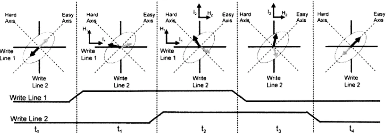
When a field is applied, the two antiparallel layer magnetizations will rotate to be approximately orthogonal to the applied field, rather than following it. A current pulse sequence is used to generate a rotating magnetic field that moves the free-layer moments through the 180-degree switch from one state to the other, as shown in Fig. 10. Both the free and fixed plates are shaped so as to favor magnetization along an axis that lies at 450
to the X and Y axis of the intersecting digit lines and bitlines, as shown. By pulsing the Y and X-axis currents unidirectionally, a rotating external magnetic field is imposed on the free plate and causes its coupled magnetization components to rotate by 1800 with respect to that of the fixed plate.
Hard Easy
Axis., Axis
Writel
Line 1I . .. .
/
SHard Easy Hard
Axis Axis Axis,
i/ I
KILLWrite Write Write Write
Line 2Line Line2 Lne2 2 2
Write Line t
Write Line 2
to tj I t2 I t3
Fig. 10. Schematic of the toggling operation of Savtchenko switching. Pulses are aj sequence designed to rotate the SAF 1800 to the opposite resistance state (Ref. F-8)
Easy A, Write Line 2 tplied in a )plied in a
Read operations are performed, as with the original MTJ-MRAM, by measuring the tunneling current, whose magnitude depends on the relative orientation of fixed moment layer and the adjacent free layer. Write operations are performed by initial read operations followed by conditional toggle operations. The toggle MTJ-MRAM therefore incurs the time penalty of a slower write operation. However, as shown in Fig. 11, the operating margins of the toggle MTJ-MRAM are much more relaxed as compared to the conventional MTJ-MRAM. Essentially, it is harder to disturb half-selected cells, which will not experience the required external rotating field, and so the upper bounds on the currents are much higher.
ii (HI [liftftfil
-~ET~l
i~Operatingti
ilt llllla
il (H1)
Fig 11. Switching map of an entire 4-Mb die showing the large operating region. (From Ref. F-8)
!
1.3.7 Spin Momentum Transfer- MRAM:
The toggle MRAM solved a few key issues with conventional MRAMs. However, the problem of scaling down to less than 60 nanometers still posed a problem. One of the significant developments that could be used to circumvent this problem is the spin-momentum-transfer effect (SMT), which was theoretically predicted in 1996 [25,26] and was experimentally observed in 2000 [27].
SMT offers the potential of orders of magnitude lower switching currents and concomitantly much lower energy per bit write. SMT works because of the net angular momentum that is carried by a spin-polarized current and the transfer of this momentum to the magnetization of the free layer. This effect becomes important when the minimum dimension of the memory cell is less than 100 nanometers and becomes more efficient as the cell size is reduced. This is the opposite of what occurs with the use of conventional magnetic field switching, for which the fields necessary to switch a nanoscale cell become larger as the size of the cell shrinks.
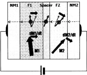
The difference between an SMT-RAM and a conventional MRAM is only in write operation mechanism, and read system is the same. A memory cell of the Spin-RAM is composed of a transistor, an MTJ, a word line (WL), a bit line (BL) and a source line (SL). An MTJ has two magnetic layers and a tunnel barrier layer between them, as shown in Fig. 12. One of the magnetic layers is switching layer, and the other is pinned its magnetization direction. A tunnel barrier layer is made of a material like crystallized MgO whose thickness is controlled less than Inm for the proper resistance area (RA) product of the MTJ. On the write operation, a WL is selected, and positive voltage is applied on a BL or a SL of a selected column. The magnetization direction of a switching layer is controlled by the current direction. On the read operation, a WL is selected, and a voltage of the order of -0.1 V is applied on a BL of a selected column.
i
~III.
Fig 12. A schematic showing the operation mechanism of spin torque transfer switching. (Ref: F-9) Quite recently, Sony Corporation fabricated and demonstrated a working model of the SMT-MRAM [28]. In their design, the authors used an STS element that has two ferromagnetic layers, F1 and F2, and a spacer layer in between them. The MTJ in this experiment consisted of a pinned layer (F1), an MgO tunnel barrier layer (Spacer) and a free magnetic layer (F2). When a spin polarized electron flows from F2 to Fl, the spin direction rotates according to the directions of magnetic moment Ml and M2. The rotation of spin direction of the electrons in F1 and F2 layer are the origin of a spin torque, dM1/ldt and dM2/dt, to the magnetic moment Ml and M2. If the given torque is large enough, magnetization of F2, M2, is reversed. Then, the magnetization of F1 and F2 transforms from parallel to anti-parallel alignment (from low resistance state to high resistance state).
According to the authors [28], the switching behavior of the Spin-RAM can be well characterized by the switching current (Ic) and the energy used for the writing process (A). Both are simplified as follows:
Ic=A *Ms2 * V
A =B * Hco * Ms * V
where A and B are constants, Ms is magnetic material parameter, Hco is anisotropic magnetic energy, and V is volume of switching layer. As MTJ size decreases, which is
NMI R " co FZ NM2
xthi < . _ _
a
*-,l·,-r
i_
•.,"IM
equivalent to smaller V, Hco value increases. Then, Ic is reduced while maintaining a
certain amount of A. Hence, smaller MTJs will be able to reduce write current according to the theory. This excellent scaling possibility is one of the most attractive features of the Spin-RAM.
Another interesting phenomenon regarding SMT is that the free layer could be rotated in both directions by reversing the direction of the current [27]. This bidirectionality is enhanced when the easy axes of the two magnetic layers have a small misalignment so that the moments of the two magnetic layers (hard and soft) are not collinear.
It appears that SMT switching can significantly improve the performance of MRAM and make it a truly universal memory. A summary of the projected performance of MRAM and SMT-MRAM is shown in the table below, which also includes entries pertaining to the performance of conventional semiconductor memories. It can be seen that SMT-MRAM has the potential to dominate the memory market, particularly because of its nonvolatility and very low power.
Standard MRAM DRAM SRAM SMT-MRAM FLASH FLASH SMT-MRAM
(90 nm)*
(90 nm)t
(90 nm)t
(90 nm)* (90 nm)t
(32 nm)t
(32 nm)*
Cell size 0.2 0.25 5 I 13 0.12 0.1 0.02 0.0 I
(pm2 ) 25 Mbicm 256 Mb/cm 64 Mblem 512 Mb/cm 512 Mb/cm 2.5 Gbi/cm 5 Gb/cm Read time 10 ns 10 os 1.1 ns 10 as 10-50 s 10-50 ns I ns Program time 5-20 ns 10 ns 1.1 ns 10 as i0. 1 100 ms 0.1 100 rnm I ns
Program energy 120 pJJ 5 p 5 pJ 0.4 pJ 30 120 n 10 al 0.02 pJ per bit Needs refresh
Fardurance >10'" >!0
I
s >101s >101 > 10" read, >10's rad, >1015
"-- 106 write >I0a 6 rite
Nonvlatilitv yes no o yes yes yes yes
1.4
Fabrication:
1. Preparation of the substrate (Fig. 13-1). To obtain ideal MTJ device performance, it
is critical to achieve atomic-scale flatness over areas of the order of the size of an MTJ. This reduces N6el coupling effects and makes a well-controlled MTJ device [29]. Substrates are thus generally prepared either with a careful silicon wafer
oxidation/cleaning or with the deposition of a dielectric such as silicon nitride on the silicon substrate, followed by a chemical-mechanical planarization (CMP) step to smooth the surface.
2. Magnetic film stack deposition (Fig. 13-2). The magnetic stack is generally composed of the following layers: a (typically nonmagnetic) seed layer to promote proper polycrystalline growth (e.g., Ta), an antiferromagnet for strong pinning of the reference layer (e.g., PtMn or IrMn), an antiferromagnetically exchange-biased pair of ferromagnets (e.g., CoFe/Ru/CoFe), the insulating tunnel barrier (e.g., A1203 or
MgO), a switchable free layer (e.g., CoFeB/Ru/CoFeB), and a suitably stable cap and hard mask layer (e.g., Ta, TaN, or TiN). Sputtering is used to deposit the metallic layers and the oxide layer is grown by reacting the metal in 02 plasma.
3. Tunneljunction patterning (Fig. 13-3). A commonly used, straightforward approach to patterning the MTJs is through the use of a conducting hard mask. Refractory materials commonly used in the semiconductor industry such as Ta, TaN, and TiN are suitable as masks for MTJ patterning. The MTJ shapes are defined in the hard mask by transfer from a first photomask level in a process like the following: apply resist/expose and develop/RIE through hard mask/strip resist. The pattern is further transferred downward to penetrate to (or through) the tunnel barrier, leaving behind a low-resistance base layer, which covers the entire wafer.
4. Dielectric encapsulation (Fig. 13-4). The encapsulation of the etched MTJs protects
them while at the same time forming the environment in which the MT wiring level will be created. The choice of encapsulation is determined from three requirements: a) it must not damage the MTJs; b) it must adhere well to the substrate; and c) it should closely emulate the interlayer dielectrics (ILDs) that would be used in a fully integrated wafer process. The dielectric thickness is chosen such that it will be thick enough to provide the environment for the wiring level above the MTJs.
5. Planarization (Fig. 13-5). The wiring process adopted is the damascene copper
wiring process and hence, the wafers generally undergo a gentle dielectric CMP process at this stage. The purpose of the CMP is to remove topography from the surface that is caused by the underlying MTJs. This step is also the first check of the adhesion of the dielectrics to the underlying metal films, as well as the cohesion of
the metal films to each other.
6. Wiring (Fig. 13-6). This final step comprises of a photomask-defined trench being
etched into the dielectric with RIE. After the trench etching and a suitable cleaning step, the wiring liner film is deposited, along with a thin copper seed layer. This deposition is followed by the electroplating of copper to completely fill the trench and provide enough overburden so that the ensuing CMP step will planarize the metal coincident with the surface of the dielectric. A post-polish cleaning of the wafers is the final preparation step before electrical testing.
Fig 13. Schematic cross-sectional representation of the basic steps involved in fabricating the short loop. The red lines represent the MTJ tunnel barrier. Source: Ref F-10
1.5 Fabrication
Issues:
To accomplish high-density MRAM, the fabrication of a sub-micron MTJ cell array sensitive to cell design and the process, must be a precedent. In light of the fabrication process, the deposition and etching of the MTJ are most critical because the layer-thickness control as well as the spatial layer-thickness uniformity is directly related to the sensing margin. Listed below are a few technical challenges that presently face the MRAM manufacturing process.
1.5.1. Resistance uniformity of sub-micron MTJ cell
The junction resistance is determined by the tunnel barrier (typically, AlOx) thickness. In particular, the resistance uniformity originating from the thickness uniformity of the
-;-- : :- - ;; ; ; i- ; ~'~-~;--- ;; ;; ---:-;; i -6.
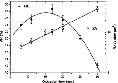
4ý
tunnel barrier is extremely important since it should distinguish the data status of either 0 or 1 within less than 50% of the resistance difference. Fig. 14 shows how sensitively MR ratio and junction resistance varies depending on the barrier plasma oxidation time. Unlike the resistance that changed linearly as a function of oxidation time, the MR ratio varied nonlinearly. Fortunately, with present day deposition systems, the uniformity of the resistance and the resistance change can be much easily controlled.
E
1
Oxidation time (sec)
Fig. 14. Variation of MR and resistance in MTJs as a function of barrier oxidation time. From IF-11].
1.5.2 Control on the Switching field:
Another major problem arises due to a spreading of the switching field. This can be avoided or at least minimized by having a very high degree of uniformity in the magnetic properties of the elements. This applies on two levels.
Firstly, the switching field required by one element must be as similar as possible to that required by another element. This requires uniformity in anisotropy across the wafer, which in turn requires identical chemical composition and processing conditions at all points on the wafer. As elements become smaller, however, the switching field will increasingly depend not only on the composition and processing of the magnetic material, but also on the precise shape of the element itself, through a phenomenon known as "Shape anisotropy". Local failures in lithography will, therefore, translate directly into variation in switching field.
The second level on which uniformity applies is the repeatability of the switching process within a single element. One of the surprising observations in the studies of MRAM-like elements is that there can be a large variation in switching field from one cycle to the next within the same element [30]. This is caused by thermal fluctuations, which allow hopping over energy barriers [31] and may select between two competing reversal mechanisms. It is possible to design out these competitions through careful choice of the element's shape. Flat-ended rectangular elements are particularly unpredictable, as the magnetization can form a C-shape, an S-shape [32], or a vortex [33] when it reaches the end of the element. Pulling the flat end of the rectangle out into a point (to form an elongated hexagon) can improve repeatability [34], although forming too sharp a point renders the element very sensitive to small changes in lithographic definition [35].
1.5.3 Half-select instability:
Stability is very important in a memory element. Of particular concern is a problem known as 'half-select instability'. During writing, all of the elements along one bit and one word line are exposed to some magnetic field. According to the Stoner-Wohlfarth astroid, this field should not be sufficiently strong to cause writing to occur, because only one of the required field components is present. These elements are said to be half-selected. However, as one approaches the astroid curve, the stability of the element against thermal fluctuations will be reduced [31]. There is concern that the half-selected elements will have an increased probability of suddenly changing data state, leading to data loss.
1.5.4 Superparamagnetism limit:
Superparamagnetism concerns the loss of magnetic stability as a result of thermal fluctuations that occur when magnetic particles are made too small. This could limit the ability of MRAM to follow Moore's law in the future. As a rule, industry will only invest in the infrastructure needed to establish a new technology if several future generations at progressively higher densities are assured.
the total volume of the magnetic particle. Interestingly, this is easily achievable, either through a change in material from magnetically soft materials, such as permalloy or CoFe, to magnetically harder materials like Fe or FePt, or, as is more probable, through making the element shape more elongated to generate strong shape anisotropy fields. The difficulty comes in then writing data to these stabilized elements: the current density that must be carried in the word and bit lines quickly exceeds the failure threshold of the tracks. Even if the track does not fail immediately, the thermal power dissipation from the chip will be greatly increased, leading to severe thermal management problems. The mathematical form of the dependence of required current density on element size is such that finding new conducting materials that have higher failure thresholds is unlikely to yield much improvement [36]. One of the proposed solution involves [37] heating the antiferromagnetic layer of the MRAM element above its Neel temperature through electrical heating from the currents in the word and bit lines, thus lowering the required write field.
1.6 Research Space of MRAM
In spite of its distinctive advantages, MRAM faces a few hurdles that must be surmounted before it can enter the commercialization stage. Some of the important difficulties are increasing the TMR values, improving the storage density and reducing the current required for switching. However, a number of potential advances in the materials used in MRAM are currently under discussion and experimentation.
At present, most of the research concentrates around increasing the magnitude of the TMR response. This would allow greater tolerances on other aspects of the design, as well as being a prerequisite for some of the future directions of MRAM. One attempt is to change the material in the insulating barrier. Alumina (A1203) has been the material of
choice for most MTJs. However, since Alumina tunnel barriers are amorphous, the maximum TMR that could be achieved is only -70% [38]. It has been predicted that crystalline tunnel barriers may give rise to much higher TSP and TMR values because of a highly spin-dependent evanescent decay of certain wave-functions, with particular transverse momentum values, across the tunnel barrier [39]. In particular, calculations for
perfectly ordered (100) oriented Fe/MgO/Fe MTJs, suggest TMR values of hundreds or even thousands of percent, for sufficiently thick MgO tunnel barriers [40,41]. Recently, such giant values were realized independently by researchers at IBM and AIST, Japan [42, 43] using crystalline MgO as the insulating barrier, where they reported TMR ratios of -300%. The impact of such discoveries on various information storage technologies would be immense; for example, MRAM with read performance an order of magnitude greater than current prototypes. This has motivated intense research activities on epitaxial MTJs grown on single-crystalline substrates using molecular beam epitaxy deposition techniques.
An alternative approach is to find a ferromagnetic material with 100% spin polarization that can be integrated into MTJs. The commonly used materials like Ni, Fe, and Co have spin polarizations of less than 80%, which means that the tunnel current is not completely shutoff when the layers are oppositely magnetized. The best devices currently have changes in resistance (called the TMR ratio) of over 40%. A class of magnetic materials called half-metallic ferromagnets [44] should, in principle, provide full polarization, since only one species has any states at the Fermi level. Potential candidate materials theoretically include [45] NiMnSb, PtMnSb, Lal-xSexMn0 3 (LSMO), and Cr02
-although experimental results to date have not been encouraging.
The TMR ratio is known to decrease with increasing bias voltage, which limits the absolute size of signal that can be obtained during read back. Inomata and coworkers [46] have demonstrated a double tunnel junction in which the TMR depends less strongly on bias voltage and therefore allows high TMR ratios even at moderate bias voltages. The increased fabrication difficulty and cost of a double junction must, however, be taken into consideration.
Efforts have also been made to improve the tolerance limits of the MRAM operation regime. Correct MTJ-MRAM operation depends critically on being able to sense changes in the tunneling current. However, the magnitude of the tunneling current depends exponentially on the thickness of the tunneling barrier. It is therefore critical to maintain tight control on the barrier thickness [47]. Differential and/or self-referencing sensing
schemes have been investigated that are inherently insensitive to the absolute tunneling current in a cell [19]. Variations in the tunneling current can also be masked by the presence of pinhole defects in the insulating barrier, which are hard to entirely avoid when the barrier thickness is less than 1.5 nm [47]. Many variations on the basic MTJ-MRAM cell structure and material composition have been investigated to improve performance and to maximize the operating margins [15, 47].
Advances have also been made in the switching methodology to make the switching robust to disturbances [18, 48] and magnetic cladding of the word lines and bit lines has been used to reduce the write current [15].
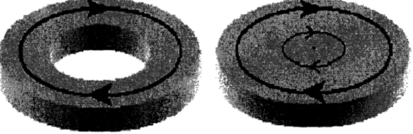
As devices scale to smaller sizes, the equilibrium magnetic states and magnetization reversal mechanisms are strongly determined by the interplay of magnetic anisotropies with the physical shape of the element. In fact, on the micrometer scale the shape of the element so fundamentally influences the switching behavior of the magnetization that a large effort has been spent with the purpose of finding the geometries that provide the simplest, fastest, and most reproducible switching mechanism, which are essential prerequisites for device applications [49, 32, 50-53]. Different geometries have been studied for this purpose, from simple circular discs [51, 54] to more advanced needle-shape elements [55]. The magnetic configuration in these elements is defined by the shape of the edges and is very sensitive to shape fluctuations and edge roughness. Thus the switching mechanism in these elements is quite complex. One possible way to overcome these complications in circular elements is to use the vortex state in which the magnetic flux is closed in the element and where the edge roughness and edge domains play a minor role. The zero stray field in this state will also favor high-density storage. However, the vortex is only stable in discs for diameters above some 100 nm [51], depending on the thickness and the material, which limits the density achievable. Moreover, the vortex formation is complex and hard to control [51, 53]. The vortex state can be made more stable if the highly energetic vortex core is removed by using the high-symmetry ring element [56] (Fig. 15), which has been proposed for use in MRAM [49, 57].
Fig. 15. Schematic representations of the vortex state in a ring and a disc. (Source: Ref. F-12) Current research on MRAMs conducted by Prof. Ross' group at MIT focuses on using a ring-shaped magnetic element which can be scaled down to the order of a few hundred nanometers [58] due to the minimal interaction between these type of elements. Further, these ring structures have the capability to store multiple bits with a high degree of reliability and are responsive to ultra-fast switching.
Two stable vortex configurations, clockwise and counterclockwise vortices, are known to exist in a ring element at remnant state. For MRAM applications, two stable vortices would be used as two distinct bit states, 0 or 1. However, specially designed conducting wires are required, as suggested in a vertical MRAM structure [59], to achieve pure vortex switching. In order to avoid the complex wiring system, an idea on magnetic switching of ring elements by an in-plane magnetic field was sought. Thus, an asymmetric ring element was proposed by a few researchers [60, 61] to meet the in-plane field switching. In this shape, magnetization reversal occurs by the motion of domain walls nucleated at a notch or naturally produced defect during the fabrication process. Recently, two stable magnetization configurations, namely "onion" states, were observed at remnant state in a narrow ring element [62]. The onion state has two symmetrical single domains with head-to-head (HTH) domain walls. A ring element with the onion state rather than the vortex state is more favorable for two-bit states in MRAM devices because it is easier to switch the onion state configuration by an in-plane applied field
[62].
Much effort is currently being focused on finding new ways to make use of the spin degree of freedom, as well as the electron's charge. A relevant example of this to the future development of MRAM is the newly discovered phenomenon of spin transfer.
First predicted in 1996 by Slonczewski [25] and Berger [26], the spin transfer effect exploits the fact that when a current flows through a ferromagnetic material, the conduction electrons become spin polarized. If these electrons then pass into another magnetic layer, there will be an interaction between the spin polarization of the carriers and the magnetization of the new host material that can lead to precession of the magnetization. An elegant experimental verification of this has recently been published [28] in which an MRAM cell was switched purely by passing an electrical current through it. No magnetic field was involved in the switching process at all. Spin transfer may provide the solution to superparamagnetism in very small MRAM elements, as a much stronger action can be generated in small elements than could be achieved through the equivalent classical magnetic field. It should, therefore, be possible to stabilize the elements against thermal fluctuations and still be able to write data. It should be noted, however, that the lithography involved in the narrow, nanoscale pillars required to access spin transfer is nontrivial.
Although SMT should contribute significantly to the write speed of MRAM, extremely large magnetoresistive ratios approaching 300% using MgO tunnel barriers [42, 43] should significantly improve the read speed. The overall expected improvement is by a factor of 2 or 3 [63]. Additionally, for performance-optimized MRAM, the overall performance could be improved by a factor of 5 to 6, that is, to 4 to 5 ns compared to 25 to 30 ns in the first MRAMs.
One of the more exotic developments of MRAM would extend its scope from purely memory into digital logic. Many of the advantages promised by MRAM (nonvolatility, radiation hardness, rapid writing, and high density) would be equally appreciated in logic devices such as microprocessors, especially for mobile or highly distributed applications. Some researchers have proposed the concept of nanoscale magnetic logic. One way of viewing this new paradigm would be as a MRAM cell that not only stores information, but can also process it - in short, MRAM that thinks. Richter and coworkers [64] have developed a reconfigurable logic system that uses MRAM cells to define the routing and functionality of the logic circuit.
1.7
Latest developments at Industry
One of the major breakthroughs in the recent times in the field of MRAM was brought out by the IBM - Infineon partnership [65] when they announced the 16 MB prototype in mid-2004. The development of a new 0.18 gm MTJ deposition equipment had made this achievement possible.
Late year before last at the IEDM (International Electron Devices Meeting), several key developments were reported by various companies. The Renesas and Mitsubishi partnership announced new developments [66] in the choice of a new magnetic material, CoFeB (ferrocobalt boron) that produces better results than with the CoFe used previously in Renesas MRAM, including a 30 to 70% higher magneto-resistance ratio.
Using these developments, it is possible to achieve data read times of 5.2ns, making the read cycle approximately 7ns. Furthermore, Renesas claims, it is the world's smallest memory cell at 0.81 square microns.
At the same conference, Toshiba, working in partnership with NEC, announced its new cell architecture based on a cross-point cell [67]. The architecture does have transistors though: it's a kind of hybrid with four cross point (CP) cells controlled by each transistor.
Toshiba says that the new cell architecture realizes a CP cell with fast read times. A typical read time of 250ns is still four times faster than for conventional CP cells, and the cells are the same size as conventional DRAM and CP MRAM.
Toshiba and NEC have also pioneered a new shape for the MTJ; a rectangle with arc shaped bulges on either side. This new shape is responsible for halving the write current compared to previous technology and it reduces write errors (despite fluctuation in the switching characteristics of the cell). The prototype is a 1Mbit chip fabricated using
130nm process technology; it operates on 1.5V.
However, one of the most exciting disclosures in the very recent past was made by Sony Corporation [28]. Late last year, Sony presented details of a type of magnetic memory that utilizes spin torque transfer to effect the switch in magnetic fields, rather than rely on
a current to switch magnetic field in the magnetic tunnel junction (MJT). Sony refers to the new MRAM device as Spin-RAM, and demonstrated a 4 kbit Spin-RAM device that was fabricated on a 180 nm process with 4 metal layers of interconnect. Sony further states that write speed as fast as 2 ns and write currents as low as 200 pA were successfully performed on the test Spin-RAM device. Also, Sony claims that the new Spin-RAM cell structure shows great promise in terms of scalability to 45 nm and future processes, and that reliability of the Spin-RAM cell has been demonstrated through more than 1012 write cycles. This was an important discovery as this brings down the write current densities (currently - 0.8 MA/cm2) to less than 1 MA/cm2 which is considered as