Assembly Lead Time Reduction in a Semiconductor Capital Equipment Plant
through Improved Material Kitting
by Sonam Jain
Bachelor of Technology in Electronics and Electrical Communication Engineering Indian Institute of Technology Kharagpur, 2008
Submitted to the Department of Mechanical Engineering O INOLOGY
in Partial Fulfillment of the Requirements for the Degree of Master of Engineering in Manufacturing
at the
LIBRARIES
MASSACHUSETTS INSTITUTE OF TECHNOLOGY September 2014
( 2014 Sonam Jain
All rights reserved
The author hereby grants to MIT permission to reproduce and to
distribute publicly paper and electronic copies of this thesis document in whole or in part in any medium now known or hereafter created.
Signature redacted
Sig n at u re of A utho r... ... ...
Sonam Jain Department of Mechanical Engineering August 15, 2014
Signature redacted_
Certified by...
red acted_
Stephen C. Graves Abraham Siegel Professor of Management Sciences Thesis Supervisor
Signature redacted,
A cce pte d by ... . ... David E. Hardt Ralph E. and Eloise F. Cross Professor of Mechanical Engineering Chairman, Committee for Graduate Student
Assembly Lead Time Reduction in a Semiconductor Capital Equipment Plant
through Improved Material Kitting
by
Sonam Jain
Submitted to the Department of Mechanical Engineering on August 15, 2014
in partial fulfillment of the requirements for the degree of
Master of Engineering in Manufacturing
Abstract
Manufacturing operations were studied at a semiconductor capital equipment manufacturing plant, with an aim to reduce the production time of their longest lead time module.
Preliminary analysis was done by observing the assembly and test operations on the production floor, and material handling operations at the warehouse. Detailed time studies were then performed on the assembly and test processes, to establish baseline measurements and to gather in-depth information on the value added and non-value added activities. It was found that 18% of the assembly activities were non-value added activities, 28% of which were related to material handling on the production floor. Based on the analysis a new kit design and kitting process were developed, which enabled parts to arrive from the warehouse in kits specific to each assembly procedure performed on the module. A method of indicating shortages was also proposed. The new design and process also facilitated Just-in-Time ordering and arrival of parts.
The new kitting process was piloted, and based on two trial runs it was found that it reduced material handling time on the production floor by 70% and overall time spent on non-value added assembly operations was reduced by 20%.
Thesis Supervisor: Stephen C. Graves
Acknowledgements
I would like to express my sincere gratitude and thank everyone who made this thesis and my journey at
MIT possible.
First and foremost, I would like to thank MIT and Varian Semiconductor Equipment Associates for giving me the opportunity to work on this project. I would like to thank my thesis advisor Professor Stephen C. Graves, for his mentorship and guidance. The thesis would not have been possible without his invaluable advice and feedback. I would also like to thank Jennifer Craig for reviewing my thesis and providing insightful feedback.
I would like to thank my supervisor Daniel Martin at Varian Semiconductor Equipment Associates for
believing in my ideas, and for his support and help in implementing them. I would like to thank Christopher Girardin, David Adkins, Jonathan Smith, Robbie Roberts, Vincent Cook, Brian McLaughlin, and Maria Doyle, who were an integral part of my project and made it possible. I would also like to thank Rusty Lake, Juan Sanchez-Caldero, Ryan Santos, Michael Ercolani, Robert Muise, Andrew Steadman, Mark Tedesco, Anthony Ciaramitaro, Gary Hoyt and Cathy Cole for their help and feedback on my project. I would also like to thank Debrework Legesse for all her help during my stay at Varian Semiconductor Equipment Associates.
I would like to sincerely thank Blake Sedore, with whom I shared several successful collaborations at
MIT, this project being one of them. He was an awesome teammate and I am grateful for all his help and support throughout my stay at MIT.
I would like to thank Professor David Hardt and Jose Pacheco for their guidance and help throughout the
program. This program provided me with a great learning opportunity and a platform to meet some amazing people. I would like to thank the other members of the M.Eng cohort, with whom I worked and socialized over the last year. They made my stay at MIT truly enjoyable. I would especially like to thank
Dale Thomas for being a great friend.
Most importantly, I would like to thank my husband for his unending support, encouragement, and patience through this intense yet exciting period of my life. I would also like to thank my parents for their love, support, and all the sacrifices they have made for me. I will be forever indebted to them.
Table of Contents
1. Introduction...13
1.1. Sem iconductor M anufacturing ... 13
1.1.1. Industry O verview ... 13
1.1.2. Sem iconductor Fabrication Process ... 14
1.1.3. Ion Im plantation... 15
1.2. Varian Sem iconductor Equipm ent Associates Background... 15
1.2.1. Prod uct Line ... 16
1.2.2. M achine Architecture... 17
1.2.3. Universal End Station Architecture ... 20
1.3. Problem Statem ent ... 21
1.3.1. M otivation ... 21
1.3.2. Problem Identification... 21
1.3.3. Approach ... 23
1.4. Thesis Organization... 24
2. Description of Current Operations ... 25
2.1. UES Production Process Overview ... 25
2.2. W orkforce Scheduling... 26
2.3. Assem bly and Test Process ... 27
2.4. M aterial Inventory ... 28
2.5. W arehouse Operations ... 29
2.5.1. Overview ... 29
2.5.2. Layout... ... 30
3. Assem bly and Testing Time Studies ... 34
3.1. Objectives ... 34
3.2. M ethodology ... 34
3.3. Assem bly Time Study ... 36
3.3.1. Data and Observations ... 36
3.3.2. Sum mary ... 39
3.4. Testing Time Study ... 40
3.4.1. Data and Observations ... 40
3.4.2. Sum mary ... 42
4. Analysis of Non-Value Added Assembly Activities ... 43
4.1. Objectives ... 43
4.2. M ethodology ... 43
4.3. Non-value Added Assem bly Activities ... 44
4.3.1. Analysis ... 44
4.3.2. Sum mary ... 47
4.4. Existing M aterial Kitting Process ... 47
4.4.1. Analysis ... 50
4.4.2. S u m m a ry ... 51
5. Theoretical Fram ework ... 52
5.1. Lean Philosophy ... 52
5.2. M aterial Feeding Systems ... 53
5.3. M aterial Kitting ... 54
5.4. Previous M IT Projects at VSEA ... 56
6. New Kitting Process ... 57
6.1. Objectives ... 57 6.2. New Kit Design Features
6.3. Design Development M ethodology ... 59
6.3.1. Sorting Parts by Sub-module ... 60
6.3.2. Sorting Parts by Size ... 62
6.3.3. Kit Design Selection ... 65
6.3.4. Kit Design Development ... 67
6.4. New Kitting Process Flow ... 68
6.5. Advantages of the New Kit Design and Kitting Process ... 70
7. Im plem entation and Results ... 72
7.1. M ethodology ... 72
7.2. Im plem entation: Phase I ... 73
7.2.1. Objectives ... 73 7.2.2. Im plementation Process ... 73 7.2.3. Results ... 74 7.2.4. Sum m ary ... 77 7.3. Im plementation: Phase 11 ... 77 7.3.1. Objectives ... 77
7.3.2. Im plem entation Process ... 77
7 .3 .3 . R e su lts ... 8 0 7.3.4. Sum m ary ... 82 7.4. Discussion ... 82 7.5. Next Steps ... 84 Recom m endations ... 86 9. Conclusions ... 88 Appendix ... 89 References ... 91
List of Figures
Figure 1: V IlSta pro d uct line ... 17
Figure 2: Schematic of ion implanter [6]... 18
Figure 3: Universal End Station schematic [8]...19
Figure 4: D M A IC m ethodology ... 23
Figure 5 UES production process flow ... 26
Figure 6: UES production floor layout ... 28
Figure 7: W arehouse layout ... 31
Figure 8: Picking and consolidation process ... 33
Figure 9 : Logboo k structure ... 35
Figure 10: Overall state of UES module during assembly [6]... 37
Figure 11: Overall UES assembly active time vs inactive time (a) including unavailable production hours (b) excluding unavailable production hours... 37
Figure 12: Overview of the assembly time study [6]... 38
Figure 13: (a) Active and Inactive time during assembly; (b) Breakdown of Active time into VA, NVA-P, and NVA-M time; (c) Breakdown of Inactive time into NVA-W and NVA-1 time... 39
Figure 14: Overall state of the module during testing [6]... 40
Figure 15: Overall UES test active time vs inactive time (a) including ECO (b) excluding ECO... 41
Figure 16: Overview of the testing time study [6] ... 41
Figure 17: (a) Active and Inactive time during testing; (b) Breakdown of Active time into VA, NVA-P, and NVA-M time; (c) Breakdown of Inactive time into NVA-W and NVA-1 time...42
Figure 18: Value added vs non-value added time per sub-module ... 45
Figure 19: Non-value activities during assembly... 46
Figure 20: Assembly production kit parts ... 49
Figure 21: Staging of production kit parts on the kit rack on UES flowline ... 49
Figure 22 :N ew Kit D esign ... 58
Figure 23: Four phases of development of the new kitting process ... 60
Figure 24: Parts distribution for existing sub-module structure ... 61
Figure 25: Parts distribution for new sub-module structure...61
Figure 27: Parts sorted by sub-module and size for the new sub-module structure... 63
Figure 28: Bin-boxes on a rack system (a) Fixed bench rack [10] (b) Mobile rack [11]... 66
Figure 29: Bin-boxes on a cart system [12]... 67
Figure 30: Modified bin-boxes on a cart system ... 68
Figure 31: Process Flow (a) Existing material handling process (b) New kitting process... 70
Figure 32: Implementation Methodology ... 72
Figure 33: Bin-boxes on a cart kit design ... 74
Figu re 34 : Final Kit D esign ... 76
Figure 35: Consolidation of parts into the kits at the warehouse ... 79
Figure 36: Cart strapped down to the truck for transportation ... 80
List of Tables
Table 1: Assembly and test times for the different modules ... 20
Table 2: Shift structure for the UES line ... 27
Table 3: Order types and warehouse order fulfillment time targets ... 32
Table 4: Z-pick kit codes for UES assembly ... 48
Table 5: Different Material Feeding Systems [16]... 53
Table 5: Size classification of parts...62
Table 6: Bin requirement per sub-module ... 64
Table 7: Overall bin requirements for existing and new sub-module structures...64
Table 8: Changes in parts ordering ... 75
1. Introduction
Varian Semiconductor Equipment and Associates (VSEA) is a wholly owned subsidiary of Applied Materials based in Gloucester, Massachusetts that designs, manufactures, markets, and services ion implantation systems, which are widely used in semiconductor fabrication. The ion implantation tool manufactured at VSEA is broadly divided into four modules- the Source, the Analyzer, the Corrector and Universal End Station (UES). These four modules are assembled and tested in parallel. The assembly and test lead time of the UES module is significantly greater than that of the other three modules, making it the bottleneck operation. This thesis describes the work done in analyzing the current assembly, test, and warehouse operations, and the implementation of an improved material kitting process, which significantly reduces the non-value added time in assembly, resulting in an overall lead time reduction of the UES module.
This section of the thesis briefly describes the semiconductor industry, the wafer manufacturing process, and the ion implantation process. It also gives a background of VSEA and describes the machine architecture of the ion implantation machine and the UES module. Finally it discusses the advantages of having a shorter lead time and the approach adopted to achieve this.
1.1. Semiconductor Manufacturing
Semiconductor manufacturing is a highly competitive business where each manufacturer seeks to provide products that consume the least power and fastest processing speed at the least cost. The industry is characterized by continuous growth, but in a cyclical pattern with high volatility with respect to demand of the products. The industry also operates on high degrees of flexibility and innovation to keep up with the rapid change of pace of the market.
1.1.1. Industry Overview
The semiconductor industry can be divided into two segments - microchip manufacturers and capital equipment manufacturers. The microchip segment produces microprocessor chips, memory chips, system on chips (SOC), and other commodity integrated circuit chips. Companies in this segment include Intel, Samsung, SK Hynix, Taiwan Semiconductor Manufacturing Company (TSMC), Analog Devices, Global Foundries etc.
The capital equipment segment manufactures equipment used in the production of microchips. This segment is further divided into two segments- Front End of the Line (FEOL) and Back End of the Line
(BEOL). In FEOL components like transistors, diodes, resistors, and capacitors are formed, while in BEOL the wires and interconnects joining the front end components are formed. VSEA traditionally has produced equipment that is used to form FEOL components. Other capital equipment manufacturers include Tokyo Electron Ltd., Axcelis Technologies, SEN Corporation etc.
1.1.2. Semiconductor Fabrication Process
Semiconductor fabrication is a complex multi-step process which involves creation of electronic circuits on a silicon wafer. This process is performed in specialized facilities called 'fabs' and takes six to eight weeks. The manufacturing process can be broadly divided into four steps- Wafer Processing, Die Preparation, IC Packaging, and IC Testing.
The process starts with growing an ingot of pure silicon, by placing a perfectly structured silicon seed into molten silicon. The molten silicon forms a chemical bond with the seed and an ingot of pure silicon, mimicking the properties of the seed, can then be pulled out as the silicon cools down. The diameter of the ingot is typically 200 mm or 300 mm. The ingot is then sawed into thin wafers and made ready for further processing.
Wafer Processing involves creation of the integrated circuits on the silicon wafer. This includes creation of transistors, capacitors, resistors, diodes, wires, and interconnects. There are several different steps and processes involved in Wafer Processing, which can be grouped into four categories- Deposition, Removal, Patterning, and Modification of Electrical Properties. Deposition involves growing, coating, or transferring material onto the wafer. Processes include Physical Vapor Deposition (PVD), Chemical Vapor Deposition (CVD), Atomic layer Deposition (ALD), and Molecular Beam Epitaxy (MBE). Removal process removes material from the wafer and includes processes like Wet Etching, Dry Etching, and Chemical Mechanical Planarization (CMP). Patterning involves shaping or altering the deposited material and is also known as Lithography. Modification involves creating transistor sources and drains through doping. Processes involved here are Ion Implantation, Furnace Annealing, and Rapid Thermal Annealing (RTA). After wafer processing the wafer is put through testing to check for damage.
Die Preparation is the step where the wafer is prepared for IC packaging and testing. It involves two steps - Wafer Mounting and Wafer Dicing. In wafer mounting the wafer is mounted on a plastic tape attached to a ring, which is then followed by wafer dicing where the wafer is cut into multiple identical rectangular pieces called dies.
IC packaging involves encasing the die in a supporting case to prevent physical damage. The case also
supports the electrical contacts that connect the device to a circuit board. The packaged chips are then put through further IC Testing to ensure that there was no damage during packaging [1].
1.1.3. Ion Implantation
Ion Implantation is a method of introducing dopants in the wafer. The purpose of doping is to introduce impurities into pure silicon that will modulate its electrical properties. A hole can be created using a p-type dopant like boron and electrons can be created by using n-p-type dopants like arsenic and phosphorous. Ion implantation is used to create p-n junctions, sources, and drains of transistors, which are the building blocks of all electronic circuits.
Ion implantation starts with creating ions of the desired element from its gas form to ensure high levels of purity. The ions are then electrostatically accelerated to high energy and made to impinge with the substrate, onto which they get implanted.
An implant is characterized by the dose and the depth of the penetration of the dopant. The dose is the integral over time of the ion current. The depth of penetration of the ions is determined by the energy of the ions, the ion species, and the composition of the substrate. Typical ion energies are in the range of 10 -500 keV and the depth of penetration is 10 nanometer to 1 micrometer [2].
1.2.Varian Semiconductor Equipment Associates Background
Varian Associates was founded in 1948, in San Carlos, California, by brothers Russell and Sigurd Varian, with the aim to commercialize the klystron technology developed by them. Klystrons are specialized linear beam vacuum tubes, used as amplifiers for electromagnetic waves at high frequencies. In 1975, it acquired Extiron Corporation, based in Gloucester, Massachusetts, which was founded in 1971 and manufactured ion implantation equipment. In 1999, the company spun out the Gloucester facility into Varian Semiconductor Equipment Associates (VSEA) [3].
Applied Materials, Inc. is a leading producer of equipment, services, and software that enable manufacture of semiconductor chips, flat panel displays, energy efficient glass, and solar photovoltaic cells. It was founded in 1967 in Santa Clara, California. Applied Materials's initial efforts were focused on developing Chemical Vapor Deposition equipment, but over the years the company has developed a wide portfolio of product offerings. In 2011, Applied Materials acquired Varian Semiconductor Equipment Associates [4].
1.2.1. Product Line
VSEA offers five different single wafer implanter products, which cover the full range of dose and energy
requirements of semiconductor doping applications. These are medium current, high current, high energy, ultra high dose, and Solion TM [5].
Medium Current implanters are characterized by low dose and very low energy of the dopant. These implanters are widely used in logic and memory chips. They provide superior overall throughput, precision doping, and high levels of contamination control.
High Current implanters are characterized by high dose and low energy of the dopant. They provide high levels of implant angle accuracy, beam steering correction, and tilt angle capability in addition to high productivity and contamination control. High current implanters are used in logic, memory, and foundry applications, especially in advanced device fabrication. High Current implanters have the highest demand among all the implanters and a steady increase in demand is anticipated, given its use in advanced microchip fabrication. In 2010 a new version of the high current implanter called the Trident was introduced, which provides high device performance, energy purity, micro-uniformity, and tight angle control.
High Energy implanters are used for low dose and very high energy applications. These implanters are primarily used in memory chip manufacturing, where increased device packing density is required. Ultra High Dose implanters are characterized by very high dose and very low energy of the dopant. This category of implanters uses a technology different from the medium current, high current, and high energy tools, in which a focused ion beam is used. Here, a plasma of the dopant is created in the chamber where the wafer is held. A pulsed DC voltage is then applied to the wafer platen which draws ions into the wafer proportional to the DC pulse. Ultra high dose doping is required in DRAM and flash memory chip fabrication.
Solion TM ion implanters were introduced in 2010 for use in solar cell manufacturing. They differ from
regular ion implanters as they handle square solar wafers, instead of round wafers. These implanters enable high throughput, in-situ patterning, and junction engineering capabilities- all of which are critical for high efficiency solar cell design.
VllSta PLATFORM
Medium Current High Current High Energy Ultra High Dose Sol ion TM
VIISta 810XP VIISta H CS VIISta H E VIISta PLAD VIISta Solion TMV
VIISta 81OXE VIISt a T ride nt VIISta 3000
VIISta 900XPT
Figure 1: VllSta product line
Demand for High Current ion implanters is the highest, followed by Medium Current and then High Energy; and within the High Current category, the Trident model is the most popular. The Trident assembly and test process is also more complex and labor intensive as compared to the other models. For these reasons, the project and thesis focus specifically on the Trident model, however the proposed improvements can be easily extended and applied to all other models.
1.2.2. Machine Architecture
VSEA's ion implanters are automated production tools that enable implantation of a single dopant species onto a silicon wafer, one wafer at a time. The ion beam is produced to a specific design criteria or process recipe using the control system. The system allows for the selection of the dopant species, dose, beam energy, implant angle, and the number of processing steps. The ion implanter consists of five modules- the Source module, the Analyzer module, the Corrector module, and the Universal End Station module, and the Equipment Front End Module (EFEM) as seen in Figure 2.
The Source module extracts and focuses the ions. Boron Trifluoride, Arsine, and Phosphine are the standard gases used by VSEA implanters to generate dopant ions. The ions are produced in a cathode source, and then extracted by creating a voltage difference between two power supplies. The ion beam is focused vertically and spread horizontally during extraction, to allow for better beam transmission to the Beamline [7].
Beam Line I
Analyzer Corrector I
9 0 = Beam Path
I*Magnet
Magnet Wafer Path
4
4-j
Facilites Process Wafer II
Facilities Gas Box Chamber H g
I I System I 0
Source Equipment Front
Source i | Universal End Station I End Module
Figure 2: Schematic of ion implanter [6]
The Beamline is where the ion beam is decelerated, focused, analyzed, measured, and made parallel. The Beamline consists of two modules- the Analyzer module and the Corrector module. In the Analyzer module, the beam leaving the source module is passed through a quad lens which focuses the beam. This focused beam then passes through the 90 degree analyzer magnet. This electromagnet creates a strong field that bends the beam by 90 degrees, to allow for the ions traveling at correct speeds (beam energy) to make it through, while eliminating undesired ions. The analyzed beam passes through two more lenses for focusing, before entering the Corrector module. This module houses a 55 degree magnet, which bends the beam by 55 degrees, so that it enters the process chamber and strikes the wafer at a 90 degree angle [7].
The Universal End Station (UES) consists of two sections - the wafer handling section and the process control section. The wafer handling section moves wafers from atmosphere to high vacuum, orients the wafer, and places it on the platen for implantation. The process control chamber interfaces with the Beamline module and is where the beam is profiled and measured, and this is where the implantation takes place. A schematic diagram of the UES module can be seen in Figure 3.
Equipment Front End Module Universal End Station
I I
Loadport I Loadlock Wafer Handler
I (Left) Robot (Left) Loadport I
Transfer I
RobprtOrienter Roplat
Loadport
Loadlock Wafer Handler Loadport II (Right) Robot (Right)
1
--Figure 3: Universal End Station schematic [8]
The wafer transport section of the UES uses the buffer robot located in the Equipment front End Module
(EFEM) to transport wafers to the load locks. The wafers are placed in the EFEM either manually or
through an automated delivery system. A mapping laser on the buffer transport robot determines the presence of wafers and then delivers them to the pass through cassette in the left or right load lock. After the mapped wafers are loaded, the load lock door closes and the load lock is pumped to high vacuum. After the high vacuum state is reached, the load lock isolation valve opens up to the wafer transfer chamber. Here another robot picks up a single wafer and transfers it onto an orienter, where the notch on the wafer is repositioned to align the crystal orientation to match the process recipe. The opposite robot arm then moves the wafer from the orienter to the platen, where it is electrostatically clamped for implantation. After implantation, the wafer is placed back in the load lock, and after all wafers in the cassette are implanted, the load lock isolation valve closes and is vented to the atmosphere. The buffer transfer robot then transfers the wafers back to the EFEM [8].
The Source, Analyzer, Corrector, and UES module are assembled and tested in parallel, and shipped separately due to size constraints. They get integrated directly at the client site, unless the client specifically requests a complete functional test, in which case they are integrated and tested at the Gloucester facility and then again broken down to the four modules for shipment. The EFEM module is a vendor supplied assembly and is not built by VSEA. The average lead times for assembly and test for each of the modules can be seen in Table 1 (the averages are based on lead times of the Tridents built between November 2013 and July 2014). UES production is evidently the bottleneck process, as its lead time is significantly larger than that of the other three modules.
Table 1: Assembly and test times for the different modules
Module Assembly Lead Time Testing Lead Time Total Lead Time
Source 2 days 2 days 4 days
Analyzer 0.6 days 0.4 days 1 day
Corrector 1.2 days 0.6 days 1.8 days
UES 5.5 days 5.4 days 10.9 days
1.2.3. Universal End Station Architecture
The Universal End Station consists of six major assemblies: the Frame, Top Process Chamber, Bottom Process Chamber, Wafer Handler, Electronics Control Rack, and Tool Control Rack. These assemblies are built independently and then integrated to form the complete UES module. After integration, the UES module is put through a series of functional tests for qualification.
Frame: The weldment frame forms the base of the UES module onto which the remaining assemblies
are mounted. The frame is a High Level Assembly (HLA) that is outsourced to an external supplier. It comes with all of the harnessing and routing done, however, some re-routing is required.
Top Process Chamber: The Top Process Chamber houses the cryo pumps (two for Trident and three in
other models) that are required to create high vacuum in the process chamber. The top process chamber also houses gate valves that are used to regulate the cryo pumps.
Bottom Chamber: The bottom process chamber houses the rotating platen (roplat). The roplat is
mounted to the tilter assembly that provides X-axis movement to adjust the implant angle. The tilter and the platen are mounted on an air bearing that provides for Y-axis movement and provides functionality for incident angle correction and multiple angle implants. The wafer is secured to the platen through electro-static clamping.
Wafer Handler: The wafer handler has three major components: the load locks, robotic arms, and the
orienter. The left and right load locks are used to hold wafers. Each load lock contains a wafer cassette platform which holds up to 25 wafers, wafer mapping lasers to detect the location of wafers in the cassette, an elevator drive to move the cassette through the laser beam for wafer mapping, a load lock isolation valve to separate the load locks from the high vacuum area of the wafer handler, and a turbo pump to create vacuum in the load locks. The robotic arms are used to move individual wafers from the cassette in the load lock to the orienter, then from the orienter to the platen for implant, and then back
to the cassette after implantation. The robot arms are driven by theta and radial motors with optical encoders for precise and repeatable positioning. The purpose of the orienter is to determine wafer eccentricity and notch position. The orienter then re-positions the notch so that the crystal orientation of the wafer matches the implant recipe. The orienter uses LEDs to establish the rotational position of the notch.
Electronics Rack: The chassis of the electronics rack is supplied with the Frame HLA. It is then removed
from the frame and built separately. It houses special power supplies and Analog-Digital-Input-Output interface modules (ADIO).
Tool Control Rack: The tool control rack houses specific control computers and control modules for the
process chamber and wafer handler.
1.3. Problem Statement 1.3.1. Motivation
The UES module is the longest lead time module in the ion implanter production process. Its lead time is significantly greater than the lead times of the other three modules, and lowering it will have several benefits.
Firstly, lowering lead time of the UES module will reduce the overall lead time of the entire machine. This will result in shorter delivery and response times to clients, making the production process more efficient.
Secondly, it will reduce the work in process inventory (WIP). The machines are high in cost and have expensive parts. Reducing WIP will result in less money tied up in in-process inventory. It will also reduce clutter on the shop floor and offer more visibility of the production flow process. Furthermore, it will reduce the risks associated with obsolescence and engineering changes.
Thirdly, in order to offer high levels of customer service, VSEA allows its customers to change or cancel their orders at any point in the production process without any penalty. Short lead times will help in reducing the risks associated with such changes.
1.3.2. Problem Identification
The problem identification process started with observing the UES production process and conducting interviews with people involved. This included the production manager, production supervisor,
production lead, production controller, manufacturing engineers, UES assemblers, UES technicians, and material handlers. Detailed time studies were then carried out to develop a deeper understanding of the process and the challenges associated with it. The details of the time studies and the observations are documented in Chapter 3 of this thesis. Analysis of the time study data resulted in identification of three major areas of improvement, each of which independently contributes towards reduction of UES lead time. The three projects
were-i) Reduction of assembly lead time through improved material kitting ii) Reduction of assembly lead time through constraint based scheduling iii) Reduction of testing lead time through optimized testing protocols
This thesis documents the work done in reduction of non-value added assembly time through kitting of parts received from the warehouse. The time study showed that 18% of the assembly labor hours are spent in non-value added activities. Of this, 28% of the time is spent in looking for parts. Approximately 200 parts are delivered from the warehouse for assembly, and these parts are not sorted by procedure or operation. Also, if there are any shortages, it is not known until the assembler specifically looks for that part. The goal of this project was to design and implement a new kitting process which would address these issues and ultimately result in reduction of the overall lead time.
Reduction of idle time through improved sequencing and scheduling of operations was looked into and documented by Sedore in his thesis [6]. The assembly time study indicated that the current grouping of tasks is not ideal, leading to dependencies between tasks across groups. Since dependencies are not clearly known, critical scheduling of tasks to achieve minimum lead time is also not known. Sedore's research focuses on re-organizing and re-grouping tasks to optimize their sequencing, and then developing build schedules for different production rates, with an aim to reduce idle time, WIP, and overall assembly the lead time.
Reduction of non-value added testing time was looked into and documented by Bhadauria in her thesis
[9]. Since most activities during testing are performed to ensure compliance and do not change the
form, fit, or function of the machine, these can be considered to be non-value added. Bhaduaria evaluates the possibility of introducing automated testing, parallel testing, and simultaneous build and test as a means to reduce the testing lead time.
1.3.3. Approach
The team adopted the DMAIC methodology as a tool for problem solving. DMAIC is a data-driven lean tool that is used to improve existing processes and is widely used in the industry. This methodology breaks down the problem solving process into five discrete ordered phases- Define, Measure, Analyze, Improve, and Control. See Figure 4.
GROUP INDIVIDUAL
- - - --- --- -- - - - - - - - - - -- - - - - - - - - -
-Figure 4: DMAIC methodology
In the Define phase, the problem was identified and the goal was defined. The project scope and resource constraints were also identified.
In the Measure phase, the existing process was studied and data was gathered to establish the baseline for future improvement. Historical data was gathered, process flow maps and value stream maps (VSM)
were drawn, and detailed time studies were performed for the assembly and test processes. The Define and Measure milestones of the project were accomplished as a group, at the end of which three potential areas of improvement were identified.
In the Analyze phase, each team member picked an area of focus and thoroughly analyzed the data gathered in the Measure phase. Gantt charts, pareto charts, and other statistical analysis tools were used, and root causes of problems were identified.
In the Improve phase, process improvement ideas were generated, developed, tested, and implemented. This included implementing a new material kitting procedure, which reduced the non-value added spent in searching and sorting parts at the production floor and the warehouse; implementing a new build schedule, which optimized sequencing of tasks and reduced idle time; and proposing a set of recommendations to reduce non-value activities in testing.
In the Control phase, measures were implemented to sustain the proposed changes. This involved creating reference documents, and updating existing documents and business systems.
1.4. Thesis Organization
The thesis has been structured in keeping with the DMAIC methodology discussed in the previous section.
Chapter 2 forms the Define section and describes the current UES production operations. It briefly describes the assembly and test process, the material flow, the workforce schedule, and the warehouse operations.
Chapter 3 forms the Measure section of the thesis and documents the time studies performed on the assembly and test processes. It states the objectives and describes the methodology for the time studies, and then presents the data gathered and observations made.
Chapter 4 forms the Analysis section of the thesis and documents the analysis of the non-value added operations in UES assembly. It analyzes the various non-value added activities with an aim to find specific areas for improvement. After establishing that material handling is the most significant non-value added activity, it analyzes the existing material handling process and identifies the inefficiencies in
it.
Chapter 5 documents the literature review performed prior to proposing and implementing any improvement steps.
Chapter 6 forms part of the Improve section and proposes a new kit design and a new kitting process. The goals for the new kitting process are defined, and the methodology used for developing it is discussed. The features of the proposed kit design and the potential advantages of the new kitting process are also discussed.
Chapter 7 forms the Improve and Control sections of the thesis. It documents the procedure followed for the implementation of the new kitting process and discusses the results. It also describes the next steps in the implementation process which need to be carried out by VSEA.
2. Description of Current Operations
2.1. UES Production Process OverviewThe production process starts with establishing a build start date, also known as the 'lay-down' date. The Material Resource Planning (MRP) system back calculates this date based on the delivery date specified by the customer and the average lead time information that is entered into the system based on historical data. The lead time of the build is measured from the lay-down date to the date that it completes testing. The lay-down rate can vary from 1 machine per day in high season to 1 machine per week in the low season.
Each machine is built-to-order and the details of the build are documented in a 'production build order' (PBO). The machines can have special features called 'options', in addition to the basic features. Machines also have 'selects', where typically one out of two available features needs to be selected. The options and selects are documented in the PBO, and the assemblers and testers use this document to build the tool. A PBO can be changed upon customer request up to 10 days before the ship date and such changes are very common.
Material inventory is stored at five different locations, and centrally coordinated using the MRP system. The inventories that feed the production line are: Supplier-managed Inventory, Warehouse Inventory, Supermarket Inventory, Gold-Square Inventory and In-line Inventory. The production lead places the order for the warehouse parts 24 hours before the scheduled laydown, and up to 5 days ahead for the supermarket parts. The supplier inventory and gold square inventory are managed through a Kanban.
On the lay-down date, building of all six assemblies starts in parallel, depending on the availability of the assemblers. Once the six assemblies are built, they are integrated, and this is followed by testing. This entire process for the Trident machine currently averages 10.9 days, with assembly and integration taking an average of 5.5 days and testing averaging 5.4 days. Once the machine completes testing, it is sent to the packaging and shipping department. The different modules - Source, Analyzer, Corrector,
UES, and the Equipment Front End Module are packaged and shipped separately. This method of
separate shipping is called 'Smart Ship'.
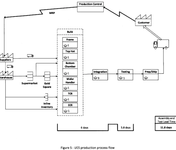
The Value Stream Map (VSM) for the current UES production process can be seen in Figure 5. It shows the process flow, material flow, and information flow during the complete UES production cycle.
Production Control Customer Buid Suppliers Warehouse Supermarket Gold I Square Inline Inventory L Bottom Wafer Handler
E-CR,-__
-_ __ _i'
Integration Testing Prep/Ship
6 days 5.8fdas
Figure 5 : UES production process flow
2.2. Workforce Scheduling
Production takes place in four shifts. On weekdays there are two 8.5 hour shifts and one 10.5-hour shift on each day, except for Friday when there are only the first two shifts. On weekends there is one 12-hour shift on each day. Each shift has a production supervisor, assemblers, and technicians. The work-force is a mix of full-time workers and contractors. The shift structure and the workwork-force distribution for the UES line can be seen in Table 2.
Asebyand
Test Lead Time
Table 2: Shift structure for the UES line
Shift No. of No. of Test Technicians
Numer Hours Days N.o ____ ________
Number Assemblers Dedicated Floating Final Test
1 7am - 3:30pm Mon -Fri 9 1 6 2
2 3pm - 11:30pm Mon -Fri 5 0 4 4
3 9pm - 7:30am Mon - Thu 5 2 0 2
Sat- Sun +
4 7am-7pm Seka Sun+_4 0 4 7
1 weekday
Due to the high variability in demand of the product, the company prefers to have its assemblers and technicians cross-trained and capable of working across different assemblies and modules. For example, within the UES cell an assembler can work on any of the assemblies- Top Chamber, Bottom Chamber, Wafer Handler, Frame etc. The testing workforce distribution is even more complicated. The testing crew is divided into three categories- technicians dedicated to the UES line, technicians that float between UES line and the 'Mixed-Mod' line where the Source, Analyzer, and Converter modules are built, and final test technicians who primarily work in the clean room but can also work on the UES line if needed. At a given point, any mix of these three categories of technicians can be assigned to work on testing of the UES module. While this structure benefits the company by enabling them to maintain a smaller work force and offering flexibility, it also makes resource planning and scheduling very challenging.
2.3. Assembly and Test Process
UES production is broadly divided into two phases: assembly and testing. Assembly can be further
broken down into build and integration. In the build phase the six assemblies (HLA Frame, Top Chamber, Bottom Chamber, Wafer Handler, ECR, and TCR) are built in parallel, typically with one assembler working on one assembly. This is followed by integration, where the built assemblies are mounted onto the frame and integrated electrically and mechanically with each other. Integration is performed by up to three assemblers, depending on their availability and workload. Assembly requires approximately 174 labor hours. Integration is followed by testing, where the module is put through a series of functional tests. This process requires approximately 59 labor hours. The average lead time for the assembly and testing of the UES is currently 10.9 days. After testing, the U ES module is sent for packaging and crating. The UES line functions as a flow line. It has designated areas for build, integration, and testing. There are two bays each for the Top Chamber build, Bottom Chamber build, and Wafer Handler build; three bays
for integration, which are also used for the frame lay-down and buildup; and nine bays for testing. Only six test bays are shown in UES production floor layout in Figure 6, as three bays are in a different location. Also, the ECR and TCR are built in a separate area on the production floor.
PICK STORAGE I
I
--
-
-- -- -
-TH1i ___ BUILD TH2 2C WHi WH2 I BC1 BC2 -- K STAG I -0 - AR I Ln- 0 FT l L - ----- ----i I INTEGRATION INTl INT2 INT3
I
I
ING EA1
I TB2 I TB4 TB6 L---GOLD SQUARE ---TBl TESTING TB3 TB5I
Figure 6 : UES production floor layout
2.4. Material Inventory
The raw material inventory for production is divided into five categories: supplier-managed inventory, warehouse inventory, supermarket inventory, Gold-Square inventory, and in-line inventory. These inventories are managed through the MRP system.
Supplier-managed inventory is the inventory of parts that are delivered directly from the supplier to the shop floor. The supplier-managed inventory is managed through a supplier kanban and includes complex HLA's such as the Frame, castings for the top chamber, bottom chamber, and wafer handler, and TCR. Suppliers for these parts are mostly local and have a turn-around time of around 2 days. The delivery of these parts is scheduled through MRP, but the production supervisor can also directly place an order for these parts with the supplier in case of an emergency.
Warehouse inventory is parts that are stored at the warehouse (Building 80) on the VSEA campus. These include large, medium and small parts that are required at the Supermarket and the assembly lines. Parts required from the warehouse are pulled 24 hours before the laydown by the production lead and production controller, through Z-picks orders and shop orders respectively. Bulk of the material required for assembly comes from the warehouse.
Supermarket inventory is inventory of the assemblies built in the supermarket. These sub-assemblies get assembled into the top level sub-assemblies. The demand for these parts is driven by shop orders. The supermarket is fed by the warehouse and also through direct deliveries from the suppliers. The supermarket in-turn feeds the gold-squares.
Gold Square inventory is the inventory of parts that are made-to-stock by the Supermarket. These are typically high volume- fast moving subassemblies and are stored in the assembly area on special racks called Gold Squares. This inventory is controlled through a visual Kanban system, managed by the planners.
In-line inventory is the inventory of parts that are stored at the assembly line. In-line inventory is further divided into two categories: 'Free Stock' or 'min-max' parts and 'Line-side' parts. Free Stock is primarily hardware parts like screws, washers, nuts, 0-rings etc., while Line-side parts are bigger parts like harness assemblies, ADIOs etc. This inventory is replenished by the warehouse. All in-line parts have a bin and a barcode associated with them. Each part also has a fixed 'order quantity' on the system depending on usage. The production lead performs a visual check of the line side bins and if the bins require more parts, he scans the barcode on them, which places an order equal to the order quantity for replenishment.
2.5. Warehouse Operations 2.5.1. Overview
The warehouse is a separate building on the VSEA campus, and is commonly referred to as 'Building 80'. It is VSEA's primary storage location and it houses large, medium, and small parts. It is responsible for fulfilling production orders, sales orders, kit room orders, window requisitions, and replenishment
orders.
Production orders are orders for parts required for assembly and testing of machines at the main building (Building 5). These are further divided into shop orders- parts required to build the base
module, and production kit orders -parts required to build a module which mostly consist of options and selects.
Sales Orders are orders for parts directly placed by the customers. These are further classified as international, domestic, or emergency orders. Sales orders are typically prioritized over other types of orders, with emergency orders being given the highest priority.
Kit Orders are orders for parts like upgrade kits, service kits, and other kits which are shipped as accessories with the ion implant machine.
Window requisitions are orders for one-off parts, such as in the case of a failure on the production floor or to replace damaged parts. Replenishment orders are used to replenish small parts stored in the main building, like in the supermarket area or in the in-line inventory on the production floor.
2.5.2. Layout
Parts are received at the warehouse from suppliers and other VSEA buildings on campus. These parts are unloaded and staged in the receiving area. Bulk parts are unloaded in the bulk staging area, barcoded, and then put away in their designated storage location. Smaller boxes are sent to the conveyor belt, where they are checked against the purchase orders. They are then either sent to the sorting and de-trash area, QA rack, or Check 80 racks. At sorting and de-trash area, the quantities are checked and the parts are made ready to be sent to the storage locations. The parts going through the
QA racks are checked at the Quality and Inspection department, before being sent for storage. Parts
which come in with missing dimensional or weight information are sent to Check 80 racks for measurement before being sent to storage.
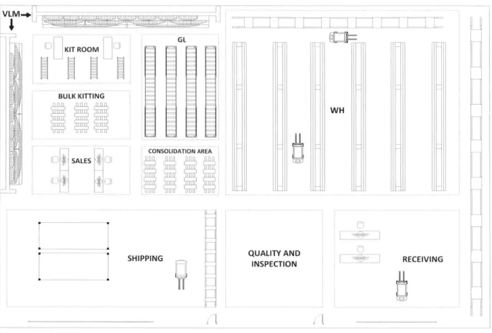
Building 80 has three primary storage locations- Warehouse (WH), General Location (GL), and VLM (Vertical Lift Module). WH holds the large and medium sized parts and is fork-lift accessible. It is further divided into sub areas called Rack (RK), Cantilever Rack (CK), and Bulk. GL holds small parts on racks, which need to be manually accessed. VLM is an automated storage system that holds fast moving small parts. It consumes very little real estate, but because of its height and design, can densely store a very large quantity of parts. See Figure 7.
VLM I GL KIT ROOM G BULK KITTING CONSOLIDATION AREA SALES
it
il I [Ll [EU SHIPPING WH QUALITY AND INSPECTIONFigure 7: Warehouse layout
There is a consolidation area with four bays. Each bay corresponds to a particular active order, and parts corresponding to this order are picked from different locations of Building 80 and dropped off here by the pickers. The parts are then consolidated, binned, and made ready for shipment. There is currently one consolidator working one regular shift in this area.
The kit room handles all kit orders, while the sales department is responsible for handling all the sales orders. They receive orders, consolidate the parts, and then complete the transaction once the orders are ready.
2.5.3. Picking Process
The picking process starts by the generation of a 'wave'. At the beginning of each shift, the warehouse coordinator checks for the open orders and generates waves for these orders based on predetermined priority. Each order type has an associated priority and a target fulfillment time. Fulfillment time is measured from the time the order is received at the warehouse to the time it takes to ship it out. The different order types, their priority, and their target fulfillment times can be seen in
RECEIVING
El
L-1
Table 3.
Table 3: Order types and warehouse order fulfillment time targets
. . Fulfillment
Priority Order Type Time t
Time Target
1 Sales - Emergency Order 5 hours
2 Sales - International Orders 5 hours 3 Sales - Domestic Orders 5 hours
4 Production- Kit Orders 24 hours
5 Production- Shop Orders 24 hours
6 Window Requisitions 48 hours
7 Transfer Orders 48 hours
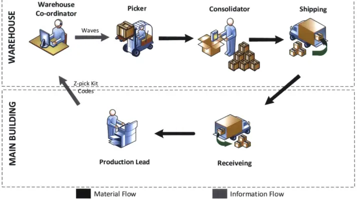
UES production orders are placed 24 hours before the scheduled laydown date through the MRP
system. The production controller places the shop orders while the production lead places the orders for the production kits. The production kits are ordered and picked using Z-pick kit codes. There are 8 pick codes associated with the UES module. Of these, 6 correspond to parts required for assembly and 2 for testing. Typically all parts associated with assembly are ordered together, as are parts for testing.
After the waves are generated at the warehouse, picking tasks are batched based on warehouse location. Pickers login to their designated zones using their scanning 'guns'. The location and quantity of the items to be picked is displayed on the gun, zone by zone. Pickers use forklifts to access parts in WH and walk to the racks in the GL location. VLM operates differently from WH and GL. There is a bin corresponding to a particular order and the all parts stored in the first VLM station are picked, and then the bin is passed onto the next station. There are 13 VLM stations in all.
I Warehouse
Co-ordinator Picker Consolidator Shipping
0 Waves
_Z-pick Kit
X
-- --- piKtod --- ---
---
-A-Production Lead Receiveing
Material Flow Information Flow
Figure 8: Picking and consolidation process
Parts are picked and dropped off at the consolidation area. The consolidator then sorts these parts based on the 'Consolidation Codes'. Consolidation Codes are codes corresponding to a particular kit code, i.e. every part associated with a given kit code has the same Consolidation Code; however each production order has a unique set of Consolidation Codes. Each production order also has unique set of 'Handling Units ' that are used for ensuring the completeness of a pick. Each kit code has three different Handling Units corresponding to the WH, GL, and VLM picks under it. If a pick is not complete, the Handling Unit flashes as 'open' on the scanning guns. Once all Handling Units are closed, it indicates that picking is complete, and final consolidation can be done. After consolidation the parts are moved to the Truck 35 staging area and made ready to be sent to Building 35 on the next available truck. Figure 8 summarizes the picking and consolidation process.
3. Assembly and Testing Time Studies
3.1.ObjectivesPreliminary analysis of the UES production process based on interviews and first person observations indicated that there were several inefficiencies in the process. It was decided that an in-depth time study would be required to develop a better understanding of the process and the issues involved. This study had three key objectives.
The first objective was to capture the time durations for each of the tasks involved in the assembly and test processes. This was necessary in order to establish baseline metrics for further analysis. The company was also interested in documenting these times in their standard work instructions.
The second objective was to observe the process and determine the time spent in value added activities and non-value added activities, and also the time that the machine was inactive during the lead time due to labor constraints or due to material shortages and failures.
The third objective was to determine the dependencies between the different tasks, in order to come up with a better grouping structure and sequence of tasks, which would maximize labor utilization and reduce idle time. This would also help determine the theoretical minimum lead time for the entire process.
3.2. Methodology
Two time studies were performed - one for assembly and another for testing. These were performed independently on two different Trident machines due to availability constraints. The time studies involved observing the complete assembly and test cycles from start to finish, by having at least one member of the team on the shop floor at any given point, throughout the duration of the study. The assembly test study took place over 6 days and the testing time study took place over 5 days.
VSEA documents its standard work instructions on a platform called Lotus Notes. Each machine has a
specific set of work instructions generated for it based on the PBO, and it is called the 'logbook'. The logbook also serves as a signoff document for the assemblers and technicians, where their signatures are captured electronically. A logbook has instructions broken down by 'modules', which are further broken down into 'sub-modules'. The sub-modules are further broken down into 'tasks'. The assemblers
and technicians sign off on individual tasks under the sub-modules. There is often a detailed procedure linked to every task for reference. Each task is accomplished through several 'steps'.
The UES module is broken down into 21 assembly sub-modules and 61 test sub-modules. The number of tasks within each sub-module varies, but there are 198 tasks in all for assembly and 1297 for testing. For the purpose of further analysis, the assembly sub-modules will be referred to as A1,A2,..,A21; and the testing sub-modules will be referred to as T1,T2,..T61. The tasks within the sub-module Al will be
referred to as A1.01, A1.02, etc., and so on. See Figure 9.
MODULE UES SUB-MODULES ASSEMBLY Al-A2- -- A21-TEST T1- -T2 -T61
-Figure 9: Logbook structure
-' -L TASKS A1.01 A1.02 A1.03 A2.01 A2.02 A2.03 A21.02 . LA 2 1.03 T1.01 T1.02 T1.03 T2.01 T2.02 T2.03 T3.01 T3.02 T3.03 L.
For the purpose of the time study, five terms were
defined-Value Added Process (VA): These were processes that changed the form, fit, and function of the
machine. Examples included - installing parts and subassemblies, making internal connections, calibrations etc.
Non- Value Added Process (NVA-P): These were processes that did not change the form, fit, or function
of the machine. All rework was classified as NVA-P. Other examples included - searching for parts, unpacking parts, cleaning parts, making facilities connections for testing, inspections and verifications etc.
Non-Value Added Movement (NVA-M): Any movement that was significant enough, during the assembly
or test process was captured as NVA-M. Examples included - movement of sub-modules or the machine itself from one part of the floor to another, movement of assembler for fetching parts that were stored far away etc.
Idle Time (/T): This was the time that a sub-module was not being worked on, once it was started. This
included scheduled and unscheduled breaks, and worker unavailability.
Wait Time (WT): This was the time the sub-module was not being worked on, once it was started,
because it was waiting on parts due to material shortages or quality issues.
During the time studies, the steps performed by the assemblers and technicians were documented, and the following information was
captured-i. Start and end times of steps
ii. Category of steps -VA,NVA-P, NVA-M, IT, or WT iii. Dependencies between tasks
iv. Recommendations for improvement based on observation and interviews
3.3.Assembly Time Study 3.3.1. Data and Observations
The time study captured the start and end times of tasks, dependencies between them, and their classification (VA,NVA-P,NVA-M,IT, WT). This information was analyzed at task level and at sub-module level and it led to five key observations.
The first observation was that the UES module overall was in an 'active' state for majority of the assembly process, as can be seen in Figure 10. The module was considered to be active when at least one of the twenty one sub-modules was being worked on. The inactive periods were attributed to unavailable production hours on weekends, overlapping breaks, and inefficient scheduling of sub-module operations. Figure 11(a) and Figure 11(b) show the percentage of active and inactive time for the overall assembly process, including unavailable production hours and excluding unavailable
production hours respectively.
Overall State of the Machine During Assembly
Active Inactive0 1 2 3 4 5 6
Figure 10: Overall state of UES module during assembly [6]
Figure 11: Overall UES assembly active time vs inactive time (a) including unavailable production hours (b) excluding unavailable production hours
Time from Start of Build (Days)
Act *Aie Active (b) Inactive (a) 0 Active NJ Inactive
The second observation was that there was a significant amount of 'inactive' time within the sub-module, i.e. the sub-module was not being worked on after it was started. Figure 12 shows the different assembly sub-modules, their relative start and end times, the active and inactive time within them, and also the dependencies between them. This inactive time within the sub-module was primarily attributed to dependencies between tasks across sub-modules which caused one module to become inactive when the prerequisite task from another sub-module was being performed. Extended breaks, part shortages,
and unavailability of personnel also contributed to the inactive time.
Assembly Time Study: Trident ES131234
Laydown and Prep Frame Wafer Handler/Load Lock Buildup Bottom Hat Buildup ECR Build Bottom Hat installation to Frame Wafer Handler/Load Lock Installation TCR Build Top Hat Buildup Roplat installation Process Chamber Liners Top Hat to Bottom Hat Installation Trough and Manifolding Tool and Electronics Rack Installation Process Chamber Buildup Scan Rotate Harness Load Lock Additions Tubing, Harnessing, and Light Links Misc End Station Items B
Gas Control Final Steps 0 = Active Inactive
_7K
1 2 3Time from Start of Build (Days)
4 5 6
Figure 12: Overview of the assembly time study [6]
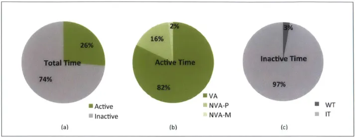
The third key observation was that on an average 82% of the active time within sub-modules was spent on value added processes (VA), while 18% was spent on non-value added activities (P and NVA-M);and 97% of the inactive time was attributed to labor unavailability (IT), while only 3% was attributed to material unavailability (WT). See Figure 13.

![Figure 2: Schematic of ion implanter [6]](https://thumb-eu.123doks.com/thumbv2/123doknet/14098139.465271/18.918.123.793.115.474/figure-schematic-ion-implanter.webp)
![Figure 3: Universal End Station schematic [8]](https://thumb-eu.123doks.com/thumbv2/123doknet/14098139.465271/19.918.102.790.112.401/figure-universal-end-station-schematic.webp)


![Figure 12: Overview of the assembly time study [6]](https://thumb-eu.123doks.com/thumbv2/123doknet/14098139.465271/38.918.99.809.328.876/figure-overview-assembly-time-study.webp)