XIII. COMMUNICATIONS BIOPHYSICS Prof. Prof. Prof. L. D. Braida S. K. Burns H. S. Colburnt Prof. L. S. Frishkopf Prof. J. L. Goldsteint Prof. J. J. Guinan, Jr Prof. R. G. Markt Prof. W. T. Peaket Prof. W. M. Siebert Prof. T. F. Weisst** Dr. I. M. Ashertt C. Bayer E. Berliner L. Bonn R. Bourk H. Conrad H. Domnitz Esquissaud E. Gorelick Hasan J. M. Arnold L. K. Brown N. B. Dowling, Jr. S. L. Foran, Jr. R. A. Gahl D. I. Geisser
Academic and Research Staff Dr. J. S. Barlowtt N. I. Durlach Dr. R. D. Hall Dr. A. J. M. Houtsma Dr. N. Y. S. Kiangt Dr. L. U. E. K6hlloffel***::- ,-Dr. H. J. Liff Dr. E. C. Moxont Dr. M. J. Mulroyf Dr. W. R. Websterf T D. W. Altmannt Graduate Students B. L. Hicks D. H. Johnson C. H. Karaian J. I. Kleinbaum M. C. Liberman*':"* R. P. Lippmann L. C. Makowski S. L. Moshier J. Myers S. Nagano Undergraduate Students R. C. Johnston J. C. Kiehl II M. Levy N. D. Megill W. Moran F. Morrison B. H. Pak R. M. Brownt D. J. Callahan A. H. Cristt B. Gaiman J. L. Henleyj $ P. W. Herman, Jr. W. F. Kelley Elizabeth M. Marrt J. M. Onorato, Jr.t L. H. Seifel J. B. Walters, Jr. Nedzelnitsky M. Oman M. Rabinowitz B. Roberts L. Smith L. Sulman Tung G. Turner, Jr. R. Willemain W. Szklannik Jean Tam J. Taylor D. A. Wade J. S. Wiley G. Woulff
This work was supported by the National Institutes of Health (Grant 5 P01 GM14940-06, the National Aeronautics and Space Administration (Grant NGL 22-009-304), Boston City Hospital Purchase Order 10656, and a grant from B-D Electrodyne Division, Becton Dickinson and Company.
TAlso at Eaton-Peabody Laboratory, Massachusetts Eye and Ear Infirmary, Cam-bridge, Mass.
Also Instructor in Medicine, Harvard Medical School, Boston, Mass.
Also Instructor in Preventive Medicine, Harvard Medical School, Boston, Mass. "Also Visiting Lecturer in Physics, University of Massachusetts, Boston, Mass. "Research Affiliate in Communication Sciences from the Neurophysiological Lab-oratory of the Neurology Service of the Massachusetts General Hospital, Boston, Mass.
Visiting Scientist from University of Stuttgart, Germany. Visiting Scientist from Monash University, Australia. 1Visiting Scientist from Albert Einstein College of Medicine.
A.
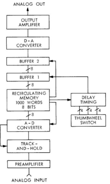
ANALOG SIGNAL DELAY
A wide-range analog signal delay has been developed that can provide delays from
1-999 ms of a signal sampled 1000 times per second with an 8-bit (1 part in 256)
reso-lution.
It is intended for use with relatively low-frequency signals that arise in
physiologic measurements that are strictly bandlimited to frequencies less than 500 Hz.
The delay is implemented by conversion
ANALOG OUT
of the input signal to an 8-bit sample, storing
the most recent 1000 samples in a
recircula-OUTPUT
AMPLIFIER
ting digital memory, and converting the sample
selected from the stored history back to a
D-ACONVERTER representative
analog output signal.
Fig-BUFFER 2
ure XIII-I is a block diagram of the system
8
and illustrates the data flow. The analog input
BUFFdrives a high-input impedance preamplifier
RECIRCULATING (10
M2) that conditions the signal to the proper
MEMORY DELAY
1000 WORDS - TIMING
range for the analog-to-digital conversion
8 THUMBWHEEL
(normally ±5
V, but adjustable from±1
to ±10).A-D SWITCH
CONVERTER Optionally, filtering could be included at this
point to eliminate the possibility of aliasing
TRACK-AND-HOLD errors. A track-and-hold circuit holds the
PREAMPLIFIER
sample value during the 200
ps
(maximum)
conversion time.
The 8-bit digital
represen-ANALOG INPUT
tation of the sampled analog signal is loaded
Fig. XIII-1.
into the recirculating memory at 1-ms
inter-Diagram of the system, illustrating
vals. A 1-second history, ending at the
cur-Diagram of the system, illustratingdata flow.
rent sample, is stored in the 1000 words of
this memory.
All samples appear at the
memory output with each complete 1-ms recirculation.
The first buffer is connected
to the memory output and its output follows the recirculating data stream until the
selected sample occurs. At this time, it ceases to follow the memory and the selected
sample is retained.
As a new sample is loaded, the sample stored in the first buffer
is transferred to the output buffer and directly converted to its analog representation.
An output amplifier provides signal conditioning and low source impedance to the analog
output connection.
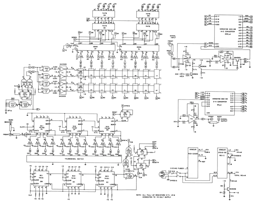
Figure XIII-2 is a schematic diagram of the entire system. The system can
be considered in several parts:
analog input,
recirculating memory,
multiple
memory buffers,
and delay timing.
Brief descriptions of each of these sections
follow.
03 Do f 3 2 I 00 7476 8y 91SI 0 61 B? 66 7475 16 164 2 93 1 " A65 7475 3E A 7 e E6 3 13 P.7 6 3 a a II T. B s 1 4 L 2 6K266 60 4266 V O 7 4 'a 10 31 6 2 I , 14 IS 11 1 56 2, T I O 1 NH 25 AS D F 48 L 2 AD T 0 FI N TI A 3 90.001 4>02 53i a+ F J L N 6 767 2TA C M T 2 6 506 36 6y4 T 01 11 IS IT IA IV 1IT 13 1 7400 7400 10.00. 5 olk CLK 5 A I N 2 2 > 8 12 -12- t 0 30 5 6 74 3 4 2 71 *0 5 I 01 I J 16 IL IN IN IF 74A 74 o CF 2 J 0.001 N30025 _12 + 00 .2 P 11 390 12 I ART 066 265063363 662 FCI 360 741 ?400C 00 1 3 13 12 IS IT 30 06 I T I 0 1 3 1 2 IS 1 7 B3 5 3
7
* Tc o S 02 3 A 14 5 6 7 0 6 1 I I 136CLK NOTEI ALL FALL-OF 6E61670
+L.- 5 +8>C +9', ONNCTE +5 +5 TO +D VO 4 1 "'2 49 + + ++ + + + + 1 02 5 6 ST T-RE T2 A 74 747 2,A .5 Of0 C 4 5 e ?Ce+ C9 C C1 1 1 2 7 4 1 14L I .2 111 4 I t41l Ill 11 141 811 11 C 1 TO EEP 'A'. 2 A TC*I 3 4 56 3 41 51 6 +5 +5 +5 +5C I C1 x I to 2 0- 0, VURTDNE D-29
Iook 5 0-A CONVERTER 50 0D
014 +1
E
015 6 Ds 0.1e7 016 *I FRONT SACIC 4T, 10k SIGNAL +0 0. OUTPUT -15ARMOUR
+V
ARMOUR
1 15V
12,13 -1 R C CHASSIS IoREP is "4.... 89 at 22 -lovn 1 TOTAL 190mA CHASSI F t 160 A 5IS 0 RIS 4.7 k IM Wo1k T SUPPLY1. Input Conversion
An integrated circuit follower provides a 10-MQ input impedance. The input range is determined by a noninverting amplifier stage with adjustable gain. A commercially obtained analog-to-digital conversion module is used for quantization. This module produces an 8-bit representation in 200
ps
(worst case); hence, a track-and-hold circuit is needed to retain the desired resolution. Since the A-D converter has an input imped-ance of 5000 , a rather simple FET switch followed by a rather large (1 mF) capacitorserves this purpose adequately. The FET switch is normally closed, but is opened by the BUSY signal produced by the A-D converter; hence, the voltage on the capacitor normally tracks the input signal and remains constant during the conversion.
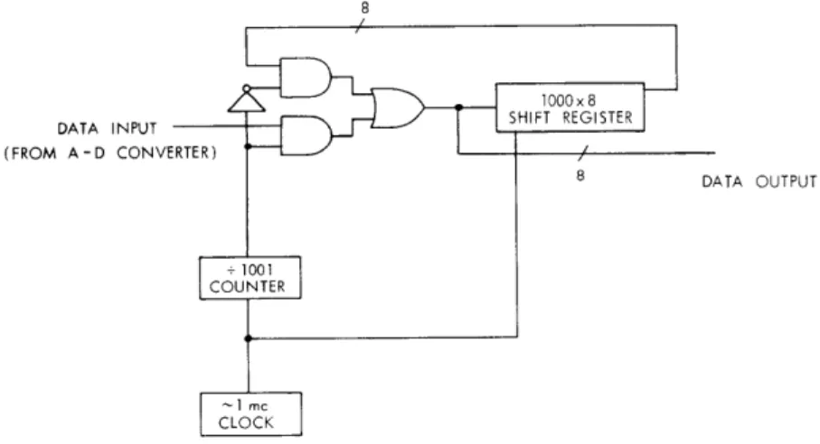
2. Recirculating Memory
A 1000 -word recirculating memory is the key element in the analog signal delay and allows selection of delays ranging from 1-999 ms. This memory is organized to accept new data at 1-ms intervals and stores the immediately previous 1000 data points in such a way that each stored datum appears sequentially, from the oldest to newest, at the output of the memory. Each stored sample will have appeared in the 1-ms inter-vals between new samples. The organization of this memory is illustrated in Fig. XIII-3.
8
1000x 8
DATA INPUT SHIFT REGISTER
(FROM A-D CONVERTER)
8 DATA OUTPUT
. 1001 COUNTER
1 mC CLOCK
Fig. XIII-3. Recirculating-memory section.
The memory is implemented by use of 16 National Semiconductor Type MM5016 500/512 bit shift registers cascaded to form 1000 8-bit words. The output of the shift register is connected to the input of a two-input multiplexer switch which is normally connected so as to cause the output of the memory to be fed back into its input. Input and output clock pulses are developed by a relaxation oscillator operating at approximately
(XIII. COMMUNICATIONS BIOPHYSICS)
2 mc (actually 2 X 1001/1000 mc) that is divided to form the necessary two-phase clocking waveform. A National Semiconductor NH0025 clock driver is used to interface the shift register. Thus data shifts through the register at half the relaxation oscillator fre-quency or ~1-mc rate and, after 1000 clock-pairs, the data have completely recirculated. With the onset of the 1001t h clock-pair the divide-by-1001 counter produces an output and causes the input of the shift register to be connected to the output of the A-D con-verter. As a result, the oldest stored sample is replaced by the just-converted sample that appears on the output of the A-D converter.
By selecting the appropriate sample, delay up to 1000 ms, corresponding to the oldest stored sample, might be selected. Selection is implemented by sampling the output of the shift register when the desired sample appears and storing its digital representation in Buffer 1, the first of two 8-bit buffer registers.
The output of the recirculating memory is, in fact, the output of the two-input multi-plexer which is also the input of the 1000-bit shift register. This choice is required if minimum delays of 1 ms are to be realized, since A-D conversion requires some time, and propagation through the memory requires exactly 1 ms.
3. Delayed Sample Buffering
Selection of the appropriately delayed sample (Fig. XIII-4) is implemented by con-tinually loading the output of the shift register into Buffer 1 until the desired sample
appears, holding this sample until recirculation is complete, and then transferring it into Buffer 2 whose output is connected directly to the input terminals of a D-A con-verter. This multiple buffering is necessary, since the delayed sample appears at the
Fig. XIII-4. Example of signal delayed 500 ms. Upper channel: undelayed original. Lower channel: delayed, quantized output.
output of the recirculating memory after the new sample is loaded.
An added virtue of using a second buffer is the synchrony of appearance of the input
and output samples. If a D-A converter with appreciable transient generation and long settling times (glitches) is used, it is desirable to use a sample-and-hold circuit in place of this all-digital buffering.
4. Delay Timing
When the memory input control connects the input to the A-D converter, the oldest stored sample appears at the output of the shift register. If we count from the terminal edge of the memory control pulse, samples s(-1000T), s(-999T), s(-998T), etc. appear at the recirculating memory output at the end of clock cycle T = 0, 1, 2, and so forth. Thus s(-mT) will appear at the end of clock cycle 1000 m. A three-decade counter, DC1, DC2, and DC3, which loads a three-digit number (m) from a thumbwheel switch, and a D flip-flop (SA) comprise the delay-timing chain. Flip-flop SA is set during the first clock cycle after the memory-load operation and connects Buffer 1 to the memory. When the decade counter overflows, SA is reset, one unit later, and causes sample s(-mT) to be retained in Buffer 1. Flip-flop SB produces a 1-unit delay so that the num-ber of the thumbwheel switch corresponds exactly to the desired delay. Flip-flop SC produces the signal to initiate another A-D conversion. SB is not used for this purpose in order to avoid a possible error caused by the nearly simultaneous sampling and clearing of the A-D converter with 1-unit delays.
5. Output Conversion
A commercially available D-A converter is used to convert the sample stored in Buffer 2 to the desired analog output voltage. Since this system is intended to operate
in conjunction with a device that samples and again quantizes these data, we decided not to interpolate further with lowpass filtering. Better transient response might be obtained by substituting a sample-and-hold circuit for the second buffer. This would, of course, necessitate modification of the signals controlling Buffer 1, unless an A-D
converter which settled in considerably less than 1
p
s were used. A buffer amplifier is placed in the output of the D-A converter to reduce the effect of circuit loading, as well as to set the output range.S. K. Burns
B.
PORTABLE CLINICAL OR LABORATORY COMPUTATION SYSTEM
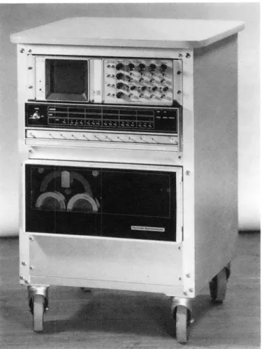
1. Introduction
A small, portable, relatively inexpensive computer system (Fig. XIII-5) has been developed for on-line use in clinical or laboratory situations. The system features an integrated hardware-software package that permits use of all peripherals, such as
(XIII. COMMUNICATIONS BIOPHYSICS)
Fig. XIII-5.
Portable clinical laboratory computation system.
interpreter constructed around the BASIC programming language.1 This report gives
a brief description of the hardware of the system. Conceptually, the system is similar
to the LINC system, which was developed in 1962.
2This was the earliest computer
sys-tem designed explicitly for application in a laboratory environment.
Since the
devel-opment of the LINC, advances in integrated circuit technology have made much more
compact and powerful systems possible.
The Analog Interface is a system of I/O devices which communicate among the
NOVA series of computers (Data General Corporation), the analog world, and the user.
In combination with the NOVA, this system provides a compact, powerful,
easy-to-operate system for processing physiologic data.
The interface consists of a 15 X 15 in.
main logic board and a 5 1/4 in. half-rack analog chassis (Fig. XIII-6). The main logic
board is inside the NOVA main frame and the analog chassis is mounted near the
NOVA main frame, sharing rack space with a small X-Y display oscilloscope
(Tektronix, Inc.).
QPR No. 106
I - -r P 4 2 C: ~f 1 -173Fig. XIII-6.
Analog chassis.
Figure XIII-7 is a block diagram of the system, which is organized around a NOVA
line processor and its associated memory. As well as the familiar teletype, special
peripherals have been added to enhance the capabilities of the system. The NOVA line
includes small general-purpose processors that are compatible from model to model.
MEMORY
NOVA LINE
CPU Fig. XIII-7.
I/O BUS
GENERL- IGGER
biagram of the
clinicallaboratory
system.TELETYPE LIN PURPOSE TRIGGER
TAPE REGTER INPUTS
ANALOG HIGH- ANALOG DISPLAY CHARACTER
RESOLUTIONCK OUPUT CHANNELS GENERATOR
CLOCK
The Central Processing Unit (CPU) is organized around 4 general-purpose registers,
two of which may be used as index registers. The NOVA shown in Fig. XIII-5 (NOVA
800)
contains 8192 16-bit words of 800-ns memory. At the bottom of the rack is a LINC tape
(Computer Operations, Inc.) that provides inexpensive and reliable storage for random
access of programs and data. A second system in current use also includes a 256K
fixed-head disk for high-speed storage and retrieval.
All of the other preipherals shown in
Fig. XIII-7 were developed in this laboratory, and will be described in more detail.
(XIII. COMMUNICATIONS BIOPHYSICS)
2.
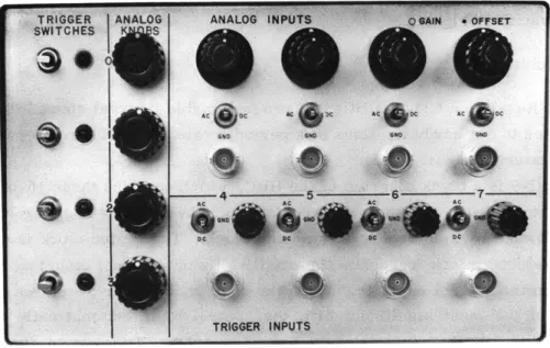
Analog Chassis Front Panel
The analog chassis front panel (Fig. XIII-8) provides a convenient point of
inter-action between the user and the system. It is divided into four sections: analog inputs,
analog knobs, trigger inputs, and trigger switches.
The analog inputs and analog knobs
provide input for 8 of the 16 available analog-input channels.
The trigger switches allow
the user to set flags in the device corresponding to switches; similarly, the trigger
inputs accept analog signals as input and set flags when the input exceeds a set threshold.
SWITCHES S
AC -C
-TRIOGER,
tOPINMrFig. XIII-8.
Analog chassis front panel.
The analog inputs accept analog signals over a range of ±0. 2 to ±4 V and allow the
user to adjust gain and offset controls to bring the signals into the normal operating
range of the analog multiplexer (±Z V).
The user may also select ac or dc signal
coupling.
The analog knobs provide a convenient method of presenting parameters to a
pro-gram. A full counterclockwise setting on a knob corresponds to minimum input, while
a full clockwise setting corresponds to maximum input.
The trigger inputs accept signals in the range ±10 V.
The user may set a threshold
voltage; if the signal exceeds this voltage, the corresponding trigger flag will be set.
The trigger circuit provides approximately 0. 25 V of hysteresis as protection against
noise.
The user may also select signal coupling at these inputs.
The trigger switches provide a convenient method of setting a program flag. They
may be depressed, in which case they spring back to the rest position when released,
or they may be pushed upward into the latch position. The switch will remain in the latch
position until the user resets it. A Light-Emitting Diode (LED) lamp is associated with each switch. These lamps are under program control, not electrically connected to the switches. While it is convenient to associate them with the state of a switch, they
may indicate any condition the user desires.
All signal inputs at the front panel are fully protected against input voltages of ±30 V. Any input signal outside the normal operating range (~ ±12 V) will activate the protective circuitry. If the protective circuitry is overloaded, the circuit will break down in such a way as to open the signal line, and thus disconnect the overload signal from the signal-conditioning electronics.
3. Special System Peripherals
a. High-Resolution Clock
The High-Resolution Clock (HRC) is a programmable interval clock. The HRC may be programmed to set hardware flags at a periodic rate, or perform interval measure-ments on an external signal.
Figure XIII-9 is a block diagram of the HRC, which contains three 16-bit registers: the preset, the counting, and the output registers. The counting register is periodically incremented by the HRC control logic's scaled clock. The scaled clock is derived by dividing the selected clock frequency (internal 1 MHz or external clock) by the clock scale factor in the control register. When the counting register overflows (produces a carry-out of the most significant bit), the control logic automatically presets the counting register with the contents of the preset register. Thus, for a given
scaled-clock frequency, the period between counter register overflows is determined by the contents of the preset register. By loading the preset register and control register with appropriate values, the user can program the counter register to overflow at precise intervals. The scaled-clock frequency selected by the user determines the basic reso-lution, while the contents of the preset register determines the interval within that resolution. The major constraints on the user are the number of available scaled-clock frequencies (four) and the fact that the counting register is 16 bits, which limits each period to 65, 536 scaled-clock cycles. In normal operation, the output register tracks the counting register to allow a readout of the current clock value.
Each time the counting register overflows, the control logic produces an HRC over-flow pulse. This overflow pulse is distributed to the other devices in the analog inter-face. This pulse allows the activity of the analog interface to be clocked at a precise, periodic rate. It is particularly useful for controlling the sampling interval on the analog-to-digital converter and the conversion intervals for the dual-channel digital-to-analog converters.
(XIII. COMMUNICATIONS BIOPHYSICS)
HIGH-RESOLUTION CLOCK
OVERFLOW PULSE
CONTROL REGISTER
CLOCK SOURCE CONTROL LOGIC
> CLOCK SCALE FACTOR
O * OVERFLOW ENABLE
Z * END ENABLE
INTERNAL 1-MHz CLOCK
STATUS FLAGS EXTERNAL CONTROL
* BUSY * EXTERNAL REFERENCE CLOCK
DONE * EXTERNAL END PULSE
" INTERRUPT DISABLE " OVERFLOW * END
* ERROR
Fig. XIII-9. High-resolution clock. Arrows indicate data and control information flow.
An Overflow Enable feature allows the HRC to request program service when the counting register overflows. By use of this feature, a program can maintain elapsed time. An End Enable feature allows the output register to be frozen upon the occurrence of an external event, and hence provides the capability of interval measurement.
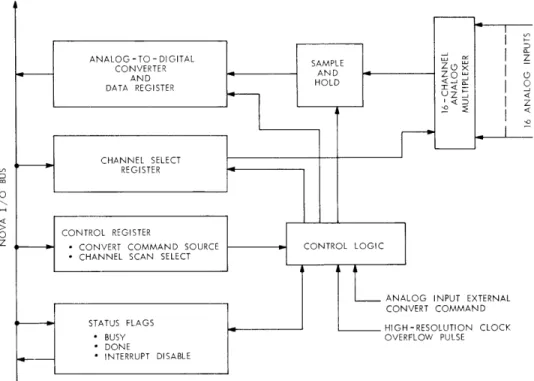
b. Analog Input
The Analog Input (AIN) provides 16 analog input channels. Any channel may be selected under program control to yield a 10-bit sample. Figure XIII-10 is a block diagram of the system. The front end of the device has channel conditioners to drive the 16-channel multiplexer. The output of the multiplexer is sampled by the Sample-and-Hold which drives the 10-bit analog-to-digital converter. The output of the analog-to-digital converter may be read in by the user. In addition to the analog section, a digital section is included containing the channel select register, the control register, the status flags, and the control logic.
The contents of the channel select register determines which of the input channels is selected by the multiplexer for the Sample-and-Hold. If the user selects the scan
mode, the content of the channel select register is automatically incremented after each conversion, so that the next sequential channel is selected.
O
O CONTROL REGISTER
Z -CONVERT COMMAND SOURCE CONTROL LOGIC
* CHANNEL SCAN SELECT
L
ANALOG INPUT EXTERNAL CONVERT COMMANDSTATUS FLAGS _ HIGH-RESOLUTION CLOCK
* BUSY OVERFLOW PULSE
SDONE
* INTERRUPT DISABLE
Fig. XIII-10. Analog input.
to specify the source of the command in order to initiate a new conversion cycle, as well as to select a scanning or nonscanning mode. The user may select, as the source of the conversion command, the program, the HRC overflow pulse, or an external control
line.
A conversion cycle comprises the following events: First, the request for a con-version cycle is noted by the hardware. When the multiplexer has selected the requested channel (as specified by the channel select register) the conversion is initiated by sam-pling the output of the multiplexer. After the Sample-and-Hold has acquired the signal and "frozen" it, the analog-to-digital converter begins the actual conversion to a digital representation. Since the Sample-and-Hold maintains the signal value, the multiplexer may be released to scan to a new channel, if this mode is selected. When the converter finishes, the AIN will indicate that a valid conversion value is available to the user.
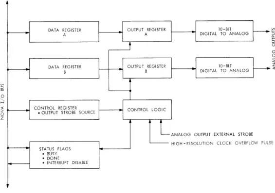
c. Dual Channel Analog Output
The Dual Channel Analog Output (AOUT) comprises two 10-bit digital-to-analog converters and the associated control logic. The AOUT (Fig. XIII-11) allows the user to generate two channels of analog output in the ±2 V range. Output conversions may be initiated under direct program control from the HRC overflow pulse, or from an exter-nal control line.
(XIII. COMMUNICATIONS BIOPHYSICS)
ANALOG OUTPUT EXTERNAL STROBE
HIGH-RESOLUTION CLOCK OVERFLOW PULSE
Fig. XIII-11. Analog output.
The data path for each channel goes from the program (by way of the NOVA bus) to the channel data register, from the data register to the output register, and finally to the 10-bit digital-to-analog converter. The user may load the data register directly, while the AOUT control logic loads the output register. While the data registers are loaded independently, the output registers are loaded by the same signal, so that any changes in output are synchronous. The control register selects the source of the signal to initiate the load signal to the output register. Status flags are provided to indicate the current status of the device and to request program service.
The use of two buffers in each channel (double buffering) allows the user to set up the desired output value in advance of the actual time it will be required, without changing the previous output value.
d. Display Hardware
The Display (DISP) provides the capability of generating displays. The DISP has two 10-bit digital-to-analog converters, and provides an addressable field of 1024 X
1024 points. As many as four X-Y display devices may be attached to the DISP output bus. The same X-Y deflection signals are applied to each device, but the devices are individually addressable for beam intensification.
with the addition of intensification logic, and interfacing to the display bus. As in the AOUT, the data registers for each channel may be independently loaded by the user.
Output registers for both channels are loaded simultaneously by the control logic. The digital-to-analog converters simply track the contents of the output registers and
con-vert the contents to an analog signal in the +2 V range. The control register permits selection of the source of the command to plot a new point, selection of the output chan-nels to be intensified, and specification of special-device options.
-DISPLAY EXTERNAL STROBE
HIGH-RESOLUTION CLOCK OVERFLOW PULSE
CHARACTER GENERATOR
Fig. XIII-12. Display diagram.
A plot cycle begins when the program senses (through the DISP status flags) the end of previous display channel activity. At this time the program loads the X-Y data registers with the position of the next point. When the DISP control logic receives a com-mand to plot the next point it loads the output registers with the contents of the corre-sponding X-Y data registers, and thus the analog outputs change. When the X-Y signals have settled to the new position, a plot command is sent to every display output device
selected in the control register. After a preset time the DISP control logic indicates that the plot cycle is complete. If a display device is not able to respond to the plot
command in the allotted time, it activates the Display Extend line. This causes the control logic to extend the cycle until the device is finished.
(XIII. COMMUNICATIONS BIOPHYSICS)
A display output device may also indicate that it is not ready to accept changes in the values of X-Y by activating the Display Wait line. The DISP control logic will not change the contents of the output registers while this signal is active, and thus prevents change in the X-Y analog signals. If the control logic receives a request to load the out-put registers while Display Wait is active, it will honor the request as soon as Display Wait becomes nonactive. Typical applications of the Wait feature are raising and lowering the pen on a hardcopy plotter or preventing writing on a storage oscilloscope while the screen is being erased.
e. Character Generator
The hardware Character Generator (CHAR) provides the user with a system for the generation of characters on the display output devices. The CHAR can represent 64 ASCII characters by a 5 X 7 dot matrix. The hardware in use at the present time is an improved version of a character generator described in an earlier report.3
Figure XIII-13 is a block diagram of the character generator. The user may access the character register, size register, and status flags. The character register speci-fies the character to be drawn, while the size register specispeci-fies the physical size of the character on the display device. The status flags are shared with the DISP logic,
CHARACTER READ-ONLY REGISTER MEMORY X DIGITAL TO ANALOG X CHARACTER SIZE DEFLECTION REGISTER RY o MULTIPLYING DIGITAL Y CHARACTER H TO ANALOG DEFLECTION
Z CHARACTER COLUMN ROW
STATUS FLAGS
BUSY CONTROL LOGIC
" DONE
* INTERRUPT DISABLE
THIS LOGIC IN THE DISPLAY
so that the user need not remember which device was the last to carry out display activity, nor need he test the status of both DISP and CHAR. All the user need do is verify that the device he wishes to use is free.
The column and row registers (which are not accessible to the user) specify the current column and row address of the dot that is to be plotted. Together with the character code, these registers provide address information for the Read Only Memory. The output of the Read Only Memory for a given character, column and row determines whether or not a dot will be drawn on the display. The column and row registers specify the relative deflections of the X and Y outputs, and thus scan the character field. In Fig. XIII- 12 the deflection signals from the CHAR are summed with the current X and Y coordinates to determine the actual position of the character on the display field.
f. General-Purpose Digital Register
The General-Purpose Digital Register (GPR) provides 16 lines of digital input and 16 lines of digital output for the user. The GPR allows the user to interface to digi-tally programmed hardware that is not used often enough to justify construction of a
special-purpose interface to the NOVA.
Figure XIII-14 is a block diagram of the GPR. A 16-bit digital output register is
USER OUTPUT INTERFACE
USER INPUT INTERFACE
(XIII. COMMUNICATIONS BIOPHYSICS)
provided. The programmer may load this register and the contents remains fixed until changed by the user. The 16-bit counting input register will accept 16 parallel digital inputs from a user interface. It may also be incremented by the user interface for use as an event counter.
The control logic allows control of the status flags by the user interface, so that the interface may request program service as would any special-purpose interface.
g. Trigger Input
The Trigger Input (TRG) provides a facility for interaction between the user and program. Four front-panel switches are provided, and when the user trips any of these switches a unique hardware flag is set which may be interrogated by the program. Analog trigger inputs are also provided. Each of these inputs allows an analog signal to set a unique trigger flag, which can be interrogated in a manner similar to the switch flags. Thus a wide variety of signals may be used to flag events for the program.
FRONT PANEL SWITCHES TRIGGER FLAGS REGISTER FRONT PANEL ANALOG TRIGGER INPUTS
M L LAMP REGISTER FRONTMPNEL
0 O
STATUS FLAGS * BUSY
* DONE CONTROL LOGIC
SINTERRUPT DISABLE * ANALOG TRIGGER ENABLE
Fig. XIII-15. Trigger input.
Figure XIII-15 is a block diagram of the TRG system. The TRG is represented on the front panel by 4 switches, 4 analog trigger inputs, and 4 LED lamps (see Fig. XIII-8).
The various inputs set flag bits in the trigger flags register. The user may load the lamp register, and thus activate a LED lamp on the front panel. The control logic responds
to changes in the status of the trigger flags register (and thus indirectly in the various
inputs) and sets the status flags to request program service.
Each of the analog trigger inputs accepts analog inputs in the ±10 V range and
com-pares the input with a reference value determined by the threshold knob (above and to
the right of the input, see Fig. XIII-8).
When the input signal exceeds the reference,
an event is said to have occurred on that input.
Thus a trigger flag is set on the
occur-rence of an event, and will remain set even after completion of the event.
If another
event occurs while the corresponding trigger flag is set, the flag will remain set.
The implementation of this system would not have been possible without the guidance
and encouragement of Professor S. K. Burns, who also designed the hardware character
generator.
The General-Purpose Register was designed by Barry Gaiman, who also
provided many useful comments about programming the system during the development
stage.
J. B. Walters, Jr.
References
1.
B. Gaiman, "A Real-time Digital Processing System for Electrophysiologic
Wave-forms," S. B. and S. M. Thesis, Department of Electrical Engineering, M. I.
T.,
September 1970.
2.
W. A. Clark and C. E. Molnar, "A Description of the LINC," in R. W. Stacy and
B. D. Waxman (Eds.), Computers in Biomedical Research, Vol. II (Academic Press,
Inc.,
New York, 1965).
3.
S.
K. Burns, "Use of a Hardware Character Generator with Small Computers,"
Quarterly Progress Report No. 98, Research Laboratory of Electronics, M. I. T.,
July 15, 1970, pp. 206-214.
C.
TIME-DOMAIN FILTERS
1. Introduction
The trend toward computer monitoring and analysis of the electrocardiogram (ECG)
has
led to the development of programmed digital filters to eliminate noise prior to
detection of the QRS complex and analysis of morphology. Multipole frequency-domain
filters are adequate for both tasks but, in general, require large amounts of processor
time.
Improved detection for the QRS complex in question can be achieved by using a
matched filter, but implementation of such a filter by correlation with a template of
a QRS complex requires many times more processor time than is required for
frequency-domain filters.
An improvement in the speed of such a filter can be accomplished by a simplification
of the template.
The QRS can be well approximated by a triangular-shaped wave of
(XIII. COMMUNICATIONS BIOPHYSICS)
similar width and height. Correlation of the incoming signal by this triangle would very closely approximate a matched filter based on the original QRS. Since the operation is
(a)
-W W
(b) Fig. XIII-16. Triangle lowpass filter.
(a) Impulse response of a tri-angle lowpass of width
w W samples.
(b) First derivative of an im-pulse response.
(c) Second derivative of an im-pulse response.
--W W
linear, the same result can be obtained by correlating with the second derivative of the triangle and then integrating the result twice. A triangle wave with a base of
2W samples is shown in Fig. XIII-16. If the height is set to W to give the triangle unity slope, the second derivative becomes simply
h"(n) = u (N-W) - 2uo(N) + uo(N+W).
Correlation of the incoming signal x(N) with the second derivative of the triangle is defined as
y"(N) = x(i) h"(i-N),
which gives
The required multiplication by two can be accomplished easily by a left-shift on a binary computer, which makes the correlation extremely fast. The final result can then be obtained by discrete integration.
y'(N) = I y"(i)
N
y(N) = C y'(i).
i-- -oo
(2)
The integration can be carried out recursively. The derivation follows from Eqs. 2 and 3.
N-1
y'(N) = C y"(i) + y"(N) i= -o00
N-1
y(N) = Z y'(i) + y'(N). i= -so
By substituting (2) and (3) in (4) and (5), we obtain
y'(N) = y'(N-1) + y"(N) y(N) = y(N-1) + y'(N).
If x(N) is a real signal, we may assume that x(N) is zero for N
<
0. Therefore, y"(N), y'(N), and y(N) are zero for N < -W:y'(N) = 0
(N < -W)
y'(N) = y'(N-1) + y"(N) (N < -W) y(N) = 0
(N < -W)
y(N) = y(N-l) + y'(N)
Equations 1 and 8-11 define a filter whose impulse implemented with no multiplicative operations.
The frequency response of this filter is just the
response is a triangle that can be
Fourier integral of the triangle wave,
F(f) = W2 sin2 (TWf)/(rWf)2
As the width of the triangle W is measured in sample intervals, f is measured in
(N < -W).
(10)
(11)
(XIII. COMMUNICATIONS BIOPHYSICS)
reciprocal sample intervals. If the sample interval is T, then the sample frequency is F = 1/T. To convert f to frequency, we must multiply by F. The spectrum of the triangle filter is shown in Fig. XIII-17. It has zeros at multiples of F/W and decreases
1 . .. ... SINC(XY)2
A
.01 i 1 1I
Fig. XIII-17. Normalized magnitude response of triangle lowpass. Gain of actual filter = W2. First zero = F/W, with F the sample rate. W = width of triangle as shown in Fig. XIII-16.
asymptotically as 1/f 2 or at 12 dB/octave. Since y(N) is a real, even function, the imaginary part of the spectrum vanishes and, therefore, the phase spectrum is zero. This is possible because the filter as shown is nonrealizable, since the output is a func-tion of input samples which have not yet occurred. This situation can be remedied by reformulating the filter so that it has a delay of W, and makes the phase spectrum
F(f) = 2TrWf.
The triangle filter has other advantages than its speed of execution. The linear phase shift means that the only phase distortion imparted to the signal is that represented by a delay of W. As it has no ringing and its impulse response is limited to 2W points,
it is easy to detect the time of an event. By choosing the sample rate to be a multiple of 60 Hz, the width of the filter can easily be arranged so that one of the zeros falls at 60 Hz, thereby eliminating power-line interference.
-2W -W 4W
W 2W
-2W
Fig. XIII-18. Impulse response of triangle2 bandpass.
(a) Two superimposed triangles in impulse response. (b) Impulse response.
(c) First derivative of impulse response. (d) Second derivative of impulse response.
to remove baseline shift. This problem can be solved by using the following filter. Two triangles of width W and 2W, with equal but opposite areas, are superimposed as shown in Fig. XIII-18. Again the heights of the triangles are adjusted so that the result-ant waveform has integral slopes. The waveform looks very much like a QRS com-plex, and, as it has zero area (zero dc component), its transform must have a zero at f = 0. In fact, its spectrum is the superposition of the spectra of the two tri-angles,
F(f) = 4W 2 (sin2 (2rWf)/(2TWf)2 - sin2 (4TrWf)/(4TrWf)2
as shown in Fig. XIII-19. Correlation with this waveform is performed as before, by correlation with its second derivative,
h"(N) = -u (N-2W) + 4u (N-W) - 6u (N) + 4u (N+W) - u (N+2W) to obtain -2W 2W -W S2W
\
1
-4S2W
w -6 -2W-W-I J/
(XIII. COMMUNICATIONS BIOPHYSICS)
y"(N) = -x(N-2W) + 4x(N-W) - 6x(N) + 4x(N+W) - x(N+2W). (12) Integration is performed using Eqs. 8-11 as before. Multiplication by 4 or 6 can be performed by a short series of addition and shift operations and no multiplications are required for implementation of this filter.
1
T
SINC( )'2-X INC(2*X2Ae,4-.ei i
•
I
Fig. XIII-19. Normalized magnitude response of triangle2 band-pass filter. Actual gain = 4W 2 First zero = F/W, with F the sample rate. W = width of filter as
shown in Fig. XIII-18.
The filter, which will be referred to as a triangle2 bandpass, falls off at approxi-mately 12 dB/octave at the low end, as can be shown from the series expansion of F(f). It also has linear phase characteristics, and therefore only minimally distorts the sig-nal. As a narrow bandpass filter it is excellent for detecting the QRS.
A highpass filter may be implemented by subtracting the output of a triangle lowpass filter from the input signal, x(N), after normalizing for the gain of the filter. The filter
is defined by
y(N) = W x(N) - Yt(N),
1 --
>--Fig. XIII-20. Normalized magnitude response of triangle highpass filter. Actual gain = W2 . To convert x axis to fre-quency, multiply x coordinate by F/W, with F the
sample rate. W = width of the triangle.
by W2 is needed to normalize the gain of the triangle lowpass, this filter can take some-what longer to execute than the previous filters unless a hardware multiply instruction
is available or unless W is a multiple of two. The filter has the frequency response shown in Fig. XIII-20 which rises like a triangle bandpass at 12 dB/octave and which has a slight ripple in the passband. Like the triangle lowpass, it has a linear phase shift and tends to distort the QRS less than a frequency-domain filter does.
2. Comparison of Frequency-Domain and Time-Domain Filters
To evaluate the effectiveness of the time-domain filters described here, they were compared with first-, second- and third-order frequency-domain filters on representa-tive sections of ECGs with varying amounts of noise. Paynter filters were chosen for comparison because the smoothness of their transient response makes them ideal for use on ECGs. The z transforms of the Paynter filters were derived by use of the bilinear transformation described by Gold and Rader,l and the results were then trans-formed into difference equations. The difference equations were then implemented2 in Real-Time BASIC on a Data General Nova 800 minicomputer. Four-second records of ECGs with combinations of muscle noise, baseline shift, and 60-Hz interference were sampled at a rate of 240 Hz and analyzed with the described highpass, lowpass,
(XIII. COMMUNICATIONS BIOPHYSICS)
and bandpass filters.
The results were then normalized to have the same maximum
deviation from the baseline as the original, and were plotted with the original for
com-parison.
ECGs with 60-Hz interference and a muscle noise were lowpass -filtered.
It was
found that second-order filters were far superior to first-order filters in removing
both
types of noise. Third-order filters were only slightly better than second-order,
how-ever. Triangle filters appeared to be approximately as effective
as third-order filters
in decreasing the maximum peak-to-peak amplitude of the noise,
which is the essential
criterion if the output of the filter is to be sent to a threshold detector.
The triangle
filters, however, left a considerable amount of low-amplitude, high-frequency
noise
in the signal, probably because of the lobes in the response of the
triangle filters
(Fig. XIII-Zl).
Somewhat different results are found when highpass filters
were run on segments
o °o- .°° l ° -. ° % .: wi1 (- --~L1 -~ A -?/r1:
I~f~~j4j
jI~
I
~i
L.rr .~~5 N i. . ir I--.2 riA 4. -pt ' 4l . c/
. -. A A - '-. 14 -- . -. (e) I f !V v V-1, -::. S~~_~4d I~Fig. XIII-21.
Lowpass filters.
(a) Four-second segment of ECG with severe muscle
noise sampled at 240 Hz.
(b) First-order lowpass at 12 Hz.
(c) Second-order lowpass at 12 Hz.
(d) Third-order lowpass at 12 Hz.
(e) Triangle lowpass, W = 10.
W
(c)
j
(XIII.
COMMUNICATIONS BIOPHYSICS)
-Io
(a) Four-second segment of ECG with baseline shift
A %(b)
First-order highpass at 6 Hz.
(d)
Third-order highpass at 6 Hz.
Fig.(
T
e)
riangle
highpass, W
=30.
of ECGs
with baseline shift. First-order filters did an admirable
sampled at Z40 Hz.
job
in
removing most
(b)
First-order highpass at 6 Hz.
(e)
Triangle highpass, W = 30.
of the artifact, and higher order filters seemed to
improve performance only slightly
(Fig. XIII-22). In
fact, in
many cases the overshoot and
ringing of the higher order
fil-ters was so objectionable that first-order filfil-ters seemed to be the best choice.
Tri-angle filters were far superior to frequency-domain filters for all cases.
The peak
amplitude of the artifact after filtering was always less with triangle highpass filters,
and they had no ringing.
Data with combinations of muscle noise, 60-Hz noise and baseline shift were
fil-tered with bandpass filters and some surprising results were found (Fig. XIII-23). The
slopes and bandwidth of the bandpass filters seem to be more important than the
center frequencies in determining their usefulness as QRS detectors.
According
to the uncertainty relation, the equivalent bandwidth and the equivalent duration of
a signal are inversely related. As the bandwidth of the bandpass filters becomes
narrower, the energy of the QRS complex becomes more spread out in time.
(XIII. COMMUNICATIONS BIOPHYSICS)
(()
o
e
s
e' u"
C f v , o
(d)
..(e)!
V " "Fig. XIII3 Bandpass filters.
.
sampled at 240 Hz.
(b) First-order highpass at 12 Hz, third-order lowpass at
12 Hz.
(c) Second-order highpass at 8 Hz, third-order lowpass at
12 Hz.
(d) Third-order highpass at 6 Hz, third-order lowpais at
12 Hz.
(e) Triangle
3bandpass, W
=
10.
Therefore, it becomes more difficult to determine the center of the complex in the noise,
and this makes narrow bandpass filters poor detectors for arrythmia monitors where the
timing of the QRS complex is important.
In order to compare quantitatively the effectiveness of the bandpass filters, several
detection algorithms were simulated with different filters used.
Triangle bandpass
fil-ters were consistently better than frequency-domain bandpass filfil-ters in detecting the
QRS.
They were also better for determining the exact time of occurrence of the QRS.
Effectiveness of the two types of filters was further compared after each was
written in Assembler language for a Nova 800 computer.
The fastest possible
imple-mentation of the filters was used even to the extent of using in-line signed multiplies
instead of calling a subroutine in the frequency-domain filters.
It was found that a
instead of calling a subroutine in the frequency-domain filters. It was found that a
triangle lowpass requires approximately 15 k±s per data point, and a triangle2 bandpass requires 20 [s per point. Frequency-domain filters without multiply hardware take considerably longer. A three-pole filter requires 250 4s per
point, and the execution time for still higher order filters was found to be roughly proportional to the number of poles. If a hardware multiply unit is added to the system, the time for a three-pole filter is approximately 67 4s per point, five times higher than a triangle lowpass.
3. Conclusion
The time-domain filters that we have described seem to be extremely effective detectors of a QRS complex. The best triangle bandpass filter for detection appears to be a triangle bandpass with F/W = 24 Hz, where F is the sample rate. The best frequency-domain detector uses a one-pole highpass at 12 Hz and a three-pole lowpass at 12 Hz and disables the detector for the T wave. If the timing of the QRS is not important, a higher order highpass at a lower frequency will improve the detector slightly.
Although triangle lowpass filters are not better in many cases than their frequency-domain counterparts, and in fact are sometimes somewhat worse, triangle highpass filters seem to be without equal. If time is not an issue, therefore, one might want to employ a triangle highpass and a three-pole lowpass in his detector.
J. M. Arnold References
1. B. Gold and C. W. Rader, Digital Processing of Signals (McGraw-Hill Book Com-pany, Inc., New York, 1969).
2. B. Gaiman, "A Real-Time Digital Processing System for Electrophysiologic Wave-forms," S. M. Thesis, Department of Electrical Engineering, M. I. T., 1970.
D. VECTORCARDIOGRAPHIC CHARACTERIZATION OF PREMATURE VENTRICULAR CONTRACTIONS
An incidence of premature ventricular contractions (PVCs) can be a serious clinical sign in cardiac patients. Frequent PVCs furnish a measure of cardiac irritability and
are often precursors of more serious cardiac conditions, such as ventricular tachycardia and ventricular fibrillation. Even an occasional PVC, under certain conditions, can be premonitory. Thus early detection of PVCs allows time to attempt to forestall more serious conditions. Considerable effort has been invested in the development of automatic detection systems for PVCs. Special-purpose hardware2 - 4 and computer
5
(XIII. COMMUNICATIONS BIOPHYSICS)
An approach employing vectorcardiography for the detection of PVCs is being developed. Theoretical aspects of our approach and some preliminary experimental results are presented in this report. This research has four interrelated goals: (i) char-acterization of myocardial electrical activity attributable to PVCs in terms of vectorcar-diograms, (ii) development of an algorithm to predict the occurrence of the next heartbeat, given past beat-to-beat times, (iii) implementation of a real-time PVC detec-tion system using the results of (i) and (ii) on a minicomputer (Data General Nova), and
(iv) evaluation of the real-time detection system with data collected in the clinic. The rudiments of vectorcardiography and the characteristics of a PVC will be out-lined. An algorithm to compute the morphological feature of a ventricular contraction defined as the "signed area vector" will be derived. The important properties of the algorithm and a practical implementation of it will be described. Some experimental results will also be presented.
1. Vectorcardiography and Premature Ventricular Contractions
The muscular contractions of the heart establish electric and magnetic fields. A single equivalent electric dipole with fixed origin is a commonly used model of myocar-dial electrical activity. T-is dipole changes its magnitude and direction with time
y- Fig. XIII-24. Vectorcardiographic axes.
as the contractile sequence progresses. A vectorcardiogram is a display of the time progression of the dipole constructed by measuring electrical potentials at the body sur-face. The vectorcardiogram is constructed from three simultaneous signals that can be viewed collectively as a time-variant three-vector. At any given time, the vector is assumed to be proportional to the equivalent electric dipole vector. Anatomical axes (Fig. XIII-24) are ordinarily used for the signals. The vectorcardiogram is viewed as an x-y plot of pairs of the component scalar waveforms. The three standard planes or projections are the frontal (xy), horizontal, (xz) and sagittal (yz) planes.
A well-defined contraction sequence occurs in the normal heart. Consequently, the equivalent electric dipole exhibits a characteristic progression during the contraction
and varies only slightly from beat to beat.
Premature ventricular contractions are
abnormal, and consequently their vectorcardiogram often looks different from that of
the normal ventricular contraction (Fig. XIII-25).
(a)
~~Z2\
Fig. XIII-25.
Scalars of vectorcardiograms for (a) normal
ventricular contraction and (b) premature ven-tricular contraction. The x components are similar, the y and z components are differ-ent. (250 ms samples.)As the name suggests, a common feature of the PVC is prematurity; that is, it comes before the next expected normal beat. Both the temporal and morphological characteris-tics of the PVC can be useful in the discrimination between normal and premature ven-tricular contractions.
The vector tip sweeps out a complicated curve in three-space as a ventricular con-traction occurs. Although the points corresponding to the beginning and the end of the ventricular contraction are seldom the same, they are usually near the origin and hence close in comparison with the deviations of the vector observed during the contraction. The planar curve corresponding to the projection of the three-dimensional curve onto a standard projection plane can be quite complex, for example, self-intersecting and not closed. The shape, direction, and relative sizes of these projected curves are of diagnostic value.6
(XIII. COMMUNICATIONS BIOPHYSICS)
morphology measure used to characterize ventricular contractions. For the moment, assume that the projected curve is closed; that is, it is a loop, and nonintersecting, (These conditions will be relaxed later.) The magnitude of the signed area of the region
enclosed by a loop is the area of the region. The sign of the area is arbitrary; a con-vention is established by observing in which direction the loop is formed (clockwise +,
counterclockwise -). (See Fig. XIII-26.)
Fig. XIII-26. Signed area, As, of a region of area A. The direction of forma-tion for the loop boundary is in-dicated by arrows.
As = -A As = A
Three parameters corresponding to the signed areas of the standard projection loops (frontal, horizontal, and sagittal) are assigned to each ventricular contraction. An algorithm to compute the signed area of a large class of loops will be derived and some of its properties discussed. Since polygons can be used to approximate continuous loops, the algorithm is specialized for computing signed areas of polygons.
2. Algorithm to Compute the Sign Area Vector
The derivation of the algorithm is based on Green's theorem of differential geometry.7 A few terms should be defined before the statement of the relationship. A region is said to be connected if every pair of points belonging to the region can be joined by a piecewise-smooth curve lying entirely within the region. A simple closed curve is a nonintersecting closed curve (loop) of a finite number of arcs joined end to end. A simply connected region has the property that every simple closed curve drawn in the interior of the region can be shrunk by a continuous deformation to a point without crossing the boundaries of R.
R
Fig. XIII-27. A simply connected region R bounded by closed curve C.
Green's theorem relates a line integral to a planar integral: Let R be a bounded sim-ply connected planar region with a simple closed curve C as its boundery (Fig. XIII-27).
Let M = M(x,y) and N = N(x, y). Assume 8M/ay and 8M/ax are continuous through-out R. Then
I am- 2-Ndxdy -C
[M(x,
y) dx + N(x, y) dy]. (1)The area, A, of the region R can be computed by appropriate choices of M(x, y) and N(x, y). Let M(x, y) = -y, and N(x, y) = x. Clearly aM/ay and
aN/ax
are continuous in R. Substitute our choices in (1). ThenaM a= -1 aN
- = +1
ay ax
S[(-l)-(+1)]dxdy
-- [y dx+x dy]R
2 dxdy = C (-y dx + x dy) R
2 A =C (-y dx + x dy)
A = (-y dx + x dy). (2)
C
Vectorcardiographic curves are parametrized by time. Consequently, (2) must be specialized for bounding curves specified parametrically. Let (x(t),y(t)), Ti < t < Tf, be a parametric description of a closed curve. Since the curve is closed, x(T.) =
1
x(Tf) and y(T) y(Tf). Assume that dx/dt and dy/dt are continuous for T. < t
<
T .dx dy
Then dx = dt and dy =dt dt, and upon substitution in (2),
1 T dx dy )
A -
Tf
-y +x-d
dt. (3)i
If the bounding curve is formed by joining arcs (a1, a2 .... an), then (3) can be modified (Fig. XIII-28):
A = -y + x - dt, (4)
Fig. XIII-28.
a3 A simply connected region bounded by a series of joined arcs (al , a2, a3, a4, a5). The area of the region is indicated.
s
A=
1
j= 1t
ftj
j-1
(
dx(t)
-y(t)
dt
+ x(t)
dy(t)
dt
)
dt.
Fig. XIII-29.Closure of a nonclosed planar curve; beginning and ending of the curve are joined by a line segment.
Fig. XIII-30.
Signed area of an intersecting curve. A is positive and A is negative.
s1 s2
Consequently I As is not the sum of the areas of the component regions.
Fig. XIII-31.
Polygonal approximation to a continuous loop.
where the arc a. is defined on the parameter interval tJ 1 < t < t.. J
The algorithm to compute the signed area (As) of a simply connected region is easily derived from the area integral (4). Only a sign convention depending on the direction of the loop need be introduced (Fig. XIII-26). Hence A s = -A, and from (4) we have
A =-A= s 2 t.
tj-1
(
dy
dx
x T- -
Y
dt
The signed area as defined in (5) was derived under the assumption that the planar bounding curves are closed and nonintersecting. Unfortunately, very few vectorcar-diography curves are closed, and some curves are intersecting. We handle these cases as follows. If the curve is not closed, we arbitrarily close it by joining the beginning and ending points of the curve by a line segment (Fig. XIII-29). If the beginning and ending of the curve are close, the overall shape of the resulting closed curve should not be grossly distorted.
An interpretation of the number derived from the signed area algorithm can be given to closed intersecting curves. The algorithm will compute a number equal to the sum of the signed areas of the component simply connected regions bounded by such a curve (Fig. XIII-30).
Loops of practical importance are polygons. Since digital processing of the vector-cardiographic signals involves sampling, the continuous loop of a projected standard is approximated by a polygon (Fig. XIII-31). If the loop is intersecting, it can be approx-imated by two or more polygons.
As the number of sides goes to infinity and the length of the largest side goes to zero,
i=3
-- (x(3), y(3))
Fig. XIII-32.
Specification of polygon vertices.
the polygon has the same signed area as the continuous loop. The number of sides approximating the loop should be large enough to approximate the signed area reasonably, but a large number of sides could impose formidable computational requirements and make roundoff errors significant in a practical implementation.
The signed area of a polygon can be computed from (5). Suppose the vertices of the polygon are (x(k), y(k)) k= 0, N
(Fig. XIII-32). Assume y(0) = y(N) and x(0) = x(N). Fortunately, the signed area of a polygon reduces to a sum of differ-ences of products
(XIII. COMMUNICATIONS BIOPHYSICS)
N
A s = [x(i) y(i-1)-y(i)x(i-1)]. (6)
i=l 1
Let u , u and u be the usual unit vectors. Let v(i) = x(i) ux and y(i) u . Then
-xy
-z
-x
-Y
(6) reduces to a sum of cross products. N
A u 1 v(i) X v(i-1). (7)
s-z
2
--i=l
3. Implementation
The three-dimensional implementation of (7) for vectorcardiographic loops is straightforward. Assume v(kT) = vx(kT) ux + v y(kT) u + v z(kT) uz, where T is the sampling period, k is the sample number, and vx(kT), v y(kT), v z(kT) are
the values of the scalar components at time kT. The signed area vector is N 1s h f A A = - v(k) x v(k-1) = Au + Au + Au , (8) -s 2 s-x s-y s-z k=1
where Ah , and A are the signed areas of the sagittal, horizontal, and frontal projections. Note that v(NT) is set equal to V(0) so that the projected curves are closed.
A few comments are in order. The integral for the signed area has conveniently reduced to a sum of cross products. The real-time implementation of (8) on a com-puter is not difficult; it requires the computation of cross products between succes-sive samples (6 multiplications and 3 subtractions). Another virtue of (8) is that the signed area vector is invariant with respect to the placement of the origin. The prac-tical implication of this invariance is that the algorithm is unaffected by the ever-present baseline shifts in an otherwise noiseless environment.
Although baseline shift does not affect the value of the signed area in a noiseless environment, the signed area becomes more sensitive to noise as the baseline value
A A
increases in magnitude. Suppose x(k) x(k) + nx(k) and y(k) - y(k) + n y(k). Assume that n (k) and n (k) are samples of uncorrelated identically distributed zero-mean
x y
2
Gaussian random variables with variance 0- . If N
A 1 a A A A
A =
j
x(k) y(k-1) - y(k) x(k-1) k=lAREA=+00590
HORIZONTAL LOOP
(a)
FRONTAL LOOP SAGITTAL LOOP
AREA =- 00954
HORIZONTAL LOOP
AREA = -00631
(b)
Fig. XIII-33. Signed areas (a) for-normal ventriculation contraction and (b) for a PVC. Arrows indicate direction of loop.
AREA =+00081