DOI 10.1007/s00542-013-2016-4 TECHNICAL PAPER
Direct imprinting of organic–inorganic hybrid materials into high
aspect ratio sub‑100 nm structures
V. J. Cadarso · T. Kiefer · V. Auzelyte · H. Atasoy · G. Gruetzner · J. Brugger
Received: 21 June 2013 / Accepted: 28 November 2013 / Published online: 11 December 2013 © Springer-Verlag Berlin Heidelberg 2013
anti-reflective (Auzelyte et al. 2012) surfaces, or to increase the sensing area in sensing applications (Heo et al. 2004; McAlpine et al. 2007). However, patterning of nanostruc-tures with HAR over large areas with a high throughput method is extremely challenging. Usually fabrication and mechanical stability issues arise when trying to obtain such structures, imposing constraints on both materials and tech-nologies (Taniguchi et al. 2010). One of the most promis-ing techniques to obtain such structures is NIL (Hirai et al.
2004; Konishi et al. 2006; Schift et al. 2009a, b). However, in the case of the fabrication of nanostructures from small recessed cavities in the master, two major issues arise dur-ing NIL process. Firstly, the complete filldur-ing of the stamp cavities becomes challenging. Further, the mechanical release of the solidified structure becomes increasingly difficult due to higher adhesion forces as a result of the increased surface area of the cavities (Dhinojwala 2003). These issues become even more dominant when releasing structures with HAR or when instead of thermal process the polymers are cross-linked by UV light, since the lack of thermal shrinkage of the nanostructures result in an even more complicated release step. These issues commonly result in damages or breakage of the released nanostruc-tures (Scheer 2013).
Inorganic–organic hybrid materials are a promising choice to overcome these issues. Concretely, Ormocer®s
offer a number of advantages, namely low material shrink-age after curing (1.5–5 %) and high chemical, thermal and mechanical stability (Klukowska et al. 2009). While the suc-cessful usability of Ormocer®s for nanoimprint has already
been shown, HAR imprint still imposes various chal-lenges. In this work, we address the challenging HAR UV-NIL of OrmoComp® (Thamdrup et al. 2008) sub-100 nm
structures using OrmoStamp® (Schift et al. 2009a, b)
working stamps fabricated from an original Si master. In
Abstract The challenging fabrication of sub-100-nm
structures with high aspect ratio by UV-nanoimprint lithography (NIL) is addressed in this work. Thermal shrinkage is induced by cooling the structures below room temperature to avoid the issues commonly arising during the release of the polymeric nanostructures from the master. The UV-NIL has been performed to obtain OrmoComp® nanostructures using OrmoStamp® working
stamps copied from Si masters. Nanoridges and nanopil-lars with 45 nm width and 380 nm thickness have been fabricated with a corresponding aspect ratio of 8.5. This is, to the best of our knowledge, the highest aspect ratio achieved using organic–inorganic hybrid materials at the sub-100-nm scale.
1 Introduction
Nanostructures with high aspect ratio (HAR) are desir-able in many areas of science and engineering, such as the development of self-cleaning (Furstner et al. 2005) or
V. J. Cadarso (*) · T. Kiefer · V. Auzelyte · J. Brugger Microsystems Laboratory, École Polytechnique
Fédérale de Lausanne (EPFL), 1015 Lausanne, Switzerland e-mail: [email protected]
J. Brugger
e-mail: [email protected] V. J. Cadarso
Laboratory for Micro- and Nanotechnology, Paul Scherrer Institut (PSI), ODRA/119, 5232 Villigen PSI, Switzerland H. Atasoy · G. Gruetzner
Micro Resist Technology GmbH, Koepenickerstr. 325, 12555 Berlin, Germany
order to prevent the defects usually observed in the fabrica-tion of these structures, a novel release step at a tempera-ture below 0 °C has been demonstrated.
2 Experimental section
2.1 Fabrication of master stamps
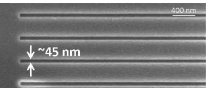
The master stamps for nanoimprinting were fabricated in silicon (Si) by electron-beam lithography (EBL) operat-ing at a 100 kV (Vistec EBPG5000) and chlorine chem-istry dry etching techniques. Hydrogen silsesquioxane (HSQ) is selected as e-beam resist in order to enhance the selectivity for HAR etch and obtain higher resolu-tion to define sub-100 nm structures. The pattern design included line and dot arrays with nominal widths rang-ing from 45 to 500 nm, and lengths from 2 up to 200 μm. Distances between the lines or respectively the dots were varied from 300 up to 2,000 nm. Figure 1 shows a scan-ning electron microscope (SEM) image of channels of 45 nm width fabricated on the master stamp. The lines are clearly defined with low roughness. The final depth of the structures was ~480 nm.
2.2 Fabrication of working stamps
The copies of working stamps were made by replication of the silicon masters into OrmoStamp® using standard
process (Schift et al. 2009a, b). OrmoStamp® offers high
UV-transparency after thermal annealing (Klukowska et al.
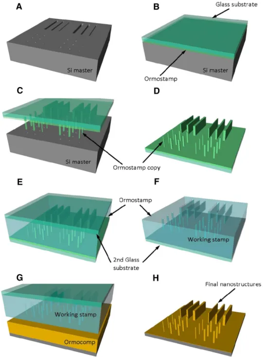
2009) and high resolution (Schift et al. 2009a, b) being suitable to be applied as UV-NIL stamps. The stamps can be further replicated and reused numerous times. The fabri-cation process is depicted in Fig. 2.
First, the silicon masters were coated with a molecu-lar layer of trichlorosilane that serves as an anti-sticking layer (Fig. 2a). A droplet of OrmoStamp® is put on top
of the silicon stamp and left at room temperature to let the polymer fill the nanocavities. Due to the rheological
properties of the nanoscale recessed areas, long wait-ing times in the range of several tens of minutes highly improved the replication quality. Then a glass slide previ-ously coated with an adhesion promoter (OrmoPrime®08)
is placed over the OrmoStamp® without additional
mechanical force, as schematized in Fig. 2b. At this point, the stack is exposed to UV light with a dose of 6,000 mJ/cm2 to induce the OrmoStamp® polymerization.
Finally the cross-linked OrmoStamp® nanostructures are
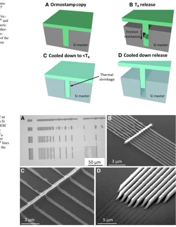
mechanically released from the Si master (Fig. 2c) and hardbaked at 130 °C. However, for HAR the release is a critical step, where material failure is caused by friction forces between the Si master and cross linked Ormo-Stamp® structures, as represented in Fig. 3a, b. In order
to prevent these defects it is proposed in this work to induce a thermal shrinkage to the nanostructures during the release step, as depicted in Fig. 3c, d, by reducing the temperature of the Si/OrmoStamp® stack. The induced
shrinkage should be large enough to overcome the rough-ness in the Si master sidewalls and to help the separation of Si/OrmoStamp® surfaces preventing the damages in
both structures. The Si/OrmoStamp® stack was therefore
cooled down below room temperature (TR) up to −8 °C prior to the release of the nanostructures. Once the Ormo-Stamp® copy is successfully released the replication
pro-cess is repeated to obtain a second OrmoStamp® copy.
Initially the first OrmoStamp® copy is silanized with a
trichlorosilane (Fig. 2d). A drop of OrmoStamp® is
depos-ited over the nanostructures and a glass substrate previ-ously coated with an adhesion promoter is placed on top (Fig. 2e). Finally the new OrmoStamp® copy is
mechani-cally released and the working stamp is ready to be used (Fig. 2f). During this second copy into OrmoStamp® no
defects were observed and the cooling release was not necessary.
2.3 OrmoComp® UV-NIL
The final nanostructures were obtained in OrmoComp®
by means of a standard UV-NIL. OrmoComp® is a
nega-tive tone material which allows for an easy surface func-tionalization, thermally stable up to 270 °C and highly transparent in the visible and near-UV ranges. The UV-NIL process starts by the spincoating of a 1 μm-thick layer of Ormocomp® on a Si wafer and the placement
of the working stamp on top (Fig. 2g). Then a pressure of 10 bar is applied for at least 5 min. to assure that the nano-cavities are filled and the stack is exposed to UV light with a dose of 6,000 mJ/cm2 in order to crosslink
the OrmoComp®. Finally the OrmoComp®
nanostruc-tures are mechanically released (Fig. 2h). The cooling process was not required to release the OrmoComp®
nanostructures. Fig. 1 Nanochannels fabricated in Si by e-beam and dry etching to
3 Results and discussion
The release of the OrmoStamp® HAR structures copy from
the Si master at TR showed a large number of defects, such as collapsed and detached lines (Fig. 4a). Figure 4b shows a SEM picture of damaged OrmoStamp® lines released at
TR. A higher magnified image of the same structures can be seen in Fig. 4c. The lines have been damaged during the release resulting in non-uniform structures. Conversely, Fig. 4d shows a SEM picture of lines well defined but with a missing section. These structures were broken during the release since it is possible to observe in the SEM image
the residues of the lines in the bottom of the layer. This shrinkage induced by the cooling below TR is additional to the process shrinkage by the curing due to exposure by UV-light, but does not include any further shrinkage due to the hardening in the hard bake (typically at 130 °C) after demoulding. Hardbaked OrmoStamp® has a linear thermal
expansion coefficient (αT) of 105 ppm/K, while the αT of Si is only 3 ppm/K. Hence, in the completely hardened stamp material, cooling down to a temperature 30 °C lower than TR induces an approximate shrinkage of the nanostructures ranging from 0.2 to 1.6 nm, with respect to the sizes of the replicated nanostructures (45–500 nm). However, since the Fig. 2 Fabrication steps:
a Silanized Si master stamp. b OrmoStamp® is casted over the Si. and a glass substrate coated with Ormoprime® is placed over the OrmoStamp® and exposed to UV light. c The OrmoStamp® copy is released from the substrate and (d) silanized. e A drop of Ormostap is placed over the first Ormo-Stamp® copy and a glass sub-strate coated with Ormoprime® is placed over the OrmoStamp® and exposed to UV light. f The second OrmoStamp® copy is mechanically released and silanized. g The second Ormo-Stamp® copy is used as working stamp in a UV-NIL process to pattern a OrmoComp® layer. h After release the OrmoComp® nanostructures are completed
release of the stamp before complete hardening is achieved, neither the contraction due to the curing is known, nor the thermal expansion coefficient of the material in its inter-mediate state. Both cases could lead to further enhanced effect. However, it should not be excluded that other effects may also participate in the cooled down release. It could be that the rapid cooling also introduces a crack in the OrmoStamp®/Silicon interface due to the large difference
between the respective αT. In any case, the release is clearly facilitated by the cooling process reducing drastically the
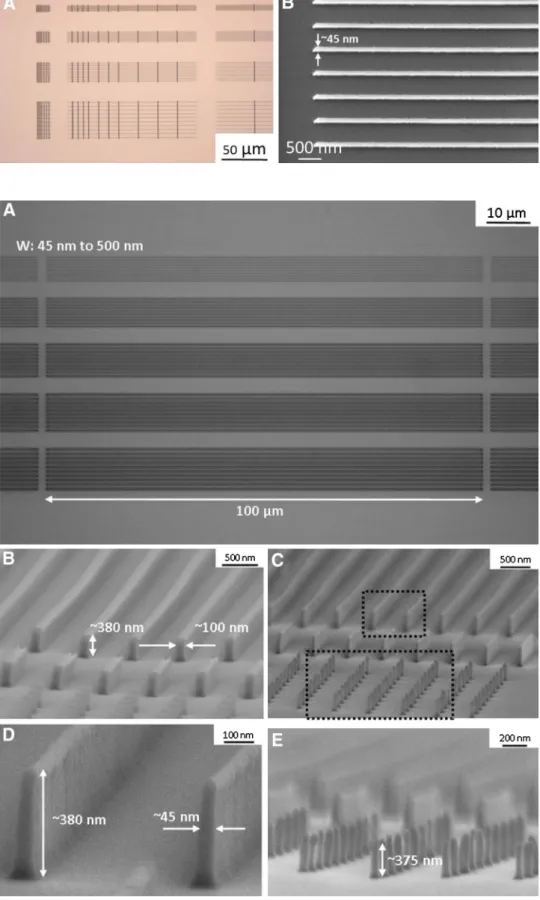
number defects in the released structures. This effect was observed in repeated experiments under the same condi-tions. Figure 5a shows an optical microscope image of an OrmoStamp® copy released using this technique (at −8 °C).
No defects or damages of the structures can be observed in this image. Figure 4e shows a SEM image of an array of ~45 nm width lines. No defects can be observed in the released structures. These results prove that the proposed cooled release can drastically improve the release of cross-linked polymeric materials from hard Si masters.
Fig. 3 Schematic
representa-tions of a the OrmoStamp® copy still in the Si master.
b The release step at TR. Fric-tion between OrmoStamp® and Si may damage the polymeric structures. c The induced ther-mal shrinkage of the Ormo-Stamp® and d the release of the shrinkage structures without defects
Fig. 4 a Optical image of an
OrmoStamp® copy from a Si master released at TR. b SEM picture of damaged Ormo-Stamp® lines released at T R.
c Zoomed view of the same
structures. d OrmoStamp® lines completely broken during the release
The results of the final released OrmoComp®
nano-structures are shown in Fig. 6. Figure 6a shows an array of 100 μm long nanoridges with increasing widths from the
top to the bottom (starting at 45 nm line-width and ending at 500 nm line-width). The distance between the each ten equal lines was 300, 500 or 1 μm, respectively. A height of Fig. 5 a Optical microscope
picture of the structures released at −8 °C and a, b SEM image of an array of lines with ~45 nm-width released at the same temperature
Fig. 6 a Optical picture of
nanoridges arrays with widths ranging from 45 (top) to 500 (bottom) nm widths. b SEM image of nanoridges 100-nm-width and 380-nm-thick structures. c SEM image of high aspect ratio nanopillars and nanoridges. d Enlarged image of the nanoridges 45-nm-width and 380-nm-thickness, corresponding to an AR of 8.5. e Enlarged image of the nanopillars
380 nm was measured both by SEM and AFM. Figure 6b shows an array of 100-nm-wide lines and pillars. The nanostructures are completely filled and no defects can be observed by SEM inspection. Figure 6c shows an array of sub-100 nm structures. All the nanoridges and the pil-lars of all lengths are well separated and do not fail across the entire length of the nanoridges. The area of the small rectangle is shown with higher magnification in Fig. 6d. The fabricated nanoridges have a height of 380 nm and a width of ~45 nm, resulting in an aspect ratio of ~8.5. The surface roughness of the sidewalls that is observed is low and hence suitable for optical or nanofluidic applications. Contrary to the larger structures, the top side of the 45-nm-width ridges is rounded. This is due to an incomplete fill-ing of the workfill-ing stamp durfill-ing the UV-NIL process, i.e. 80 % of the original depth. The large rectangle in Fig. 6c is magnified into Fig. 6e. The nanopillar arrays show a good structure replication quality without collapsed structures. These structures also exhibit a rounded top and their height is slightly smaller (~375 nm) compared to the nanoridges, which supports the hypothesis that the nanocavities nar-rower than 100 nm were not completely filled. Increas-ing the fillIncreas-ing time or workIncreas-ing with diluted version of the Ormocer® materials should improve these results.
Never-theless, an aspect ratio of 8.5 is, to the best of our knowl-edge, the highest aspect ratio obtained for sub-100-nm Ormocer® structures.
4 Conclusions
In summary, novel inorganic organic hybrid polymers were used to fabricate transparent stamp copies with HAR for UV-NIL. In order to improve the release of sub-100-nm structures polymeric structures with HAR from the Si mas-ter, a novel release step done at a temperature lower than TR has been proposed and demonstrated. Finally a poly-meric working stamp has been used in a UV-NIL process to fabricate the final nanostructures in OrmoComp®. Up
to 200 μm long nanoridges and posts with dimensions below 50 nm were obtained. This proof-of-concept experi-ment also shows the potential of carefully controlling the thermal properties of the imprinted material to facilitate the demoulding step, which is normally a major source of errors. In analogy to this effect, a UV-NIL imprint which is carried on at 20–30 °C above the room temperature can provide with the enough thermal contraction after cooling
down to room temperature, which will be investigated in a future work. This method has the potential to become a standard processing step for imprinting HAR nanostruc-tures by combined thermal and UV-NIL in the industry. The materials showed excellent results for aspect ratios up to 8.5 and thus prove their potential for fabrication of HAR nanometre structures for a variety of applications such as anti-reflective surfaces, self-cleaning surfaces or sensing applications.
References
Auzelyte V, Flauraud V, Cadarso VJ, Kiefer T, Brugger J (2012) Bio-mimetic soft lithography on curved nanostructured surfaces. Microelectron Eng 97:269–271
Dhinojwala A (2003) Nanorheology of confined fluids. Mater Sci Technol 19:021802
Furstner R, Barthlott W, Neinhuis C, Walzer P (2005) Wetting and self-cleaning properties of artificial superhydrophobic surfaces. Langmuir 21:956–961
H.-C., Scheer, High aspect ratio NIL challenges and possibilities, 10th International workshop on high aspect ratio micro and nano sys-tems technology, Berlin, April 2013
Heo YW, Norton DP, Tien LC, Kwon Y, Kang BS, Ren F, Pearton SJ, LaRoche JR (2004) ZnO nanowire growth and devices. Mater Sci Eng: R: Rep 47:1–47
Hirai Y, Konishi T, Yoshikawa T, Yoshid S (2004) Simulation and experimental study of polymer deformation in nanoimprint lithography. J Vac Sci Technol B 22:6
Klukowska A, Kolander A, Bergmair I, Mühlberger M, Leichtfried H, Reuther F, Grützner G, Schöftner R (2009) Novel transparent hybrid polymer working stamp for UV-imprinting. Microelectron Eng 86:697–699
Konishi T, Kikuta H, Kawata H, Hirai Y (2006) Multi-layered resist process in nanoimprint lithography for high aspect ratio pattern. Microelectron Eng 83:869–872
McAlpine MC, Ahmad H, Wang D, Heath JR (2007) Highly ordered nanowire arrays on plastic substrates for ultrasensitive flexible chemical sensors. Nat Mater 6:379–384
Schift H, Spreu C, Schleunitz A, Gobrecht J, Klukowska A, Reuther F, Gruetzner G (2009a) Easy mask-mold fabrication for com-bined nanoimprint and photolithography. J Vac Sci Technol, B 27:2850
Schift H, Spreu C, Saidani M, Gobrecht J, Klukowska A, Reuther F, Gruetzner G, Solak HH (2009b) Transparent hybrid poly-mer stamp copies with sub-50-nm resolution for thermal and UV-nanoimprint lithography. J Vac Sci Technol, B 27:2846 Taniguchi J, Kamiya Y, Ohsaki T, Sakai N (2010) Technique for
trans-fer of high-density, high-aspect-ratio nanoscale patterns in UV nanoimprint lithography and measurements of the release force. Microelectron Eng 87:859–863
Thamdrup LH, Klukowska A, Kristensen A (2008) Stretching DNA in polymer nanochannels fabricated by thermal imprint in PMMA. Nanotechnology 19:125301