HAL Id: hal-01763391
https://hal.archives-ouvertes.fr/hal-01763391
Submitted on 18 Jun 2019
HAL is a multi-disciplinary open access
archive for the deposit and dissemination of
sci-entific research documents, whether they are
pub-lished or not. The documents may come from
teaching and research institutions in France or
abroad, or from public or private research centers.
L’archive ouverte pluridisciplinaire HAL, est
destinée au dépôt et à la diffusion de documents
scientifiques de niveau recherche, publiés ou non,
émanant des établissements d’enseignement et de
recherche français ou étrangers, des laboratoires
publics ou privés.
Enhanced nonlinear optical response from individual
silicon nanowires
Peter Wiecha, Arnaud Arbouet, Houssem Kallel, Priyanka Periwal, Thierry
Baron, Vincent Paillard
To cite this version:
Peter Wiecha, Arnaud Arbouet, Houssem Kallel, Priyanka Periwal, Thierry Baron, et al.. Enhanced
nonlinear optical response from individual silicon nanowires. Physical Review B: Condensed
Mat-ter and MaMat-terials Physics (1998-2015), American Physical Society, 2015, 91 (12),
�10.1103/Phys-RevB.91.121416�. �hal-01763391�
Peter R. Wiecha1,2, Arnaud Arbouet1, Houssem Kallel1,2, Priyanka Periwal3, Thierry Baron3, and Vincent Paillard1,2∗ 1 CEMES-CNRS, 29 rue Jeanne Marvig, 31055 Toulouse cedex 4, France
2
U niversit´e de Toulouse, U niversit´e Paul Sabatier, 118 route de Narbonne, 31062 Toulouse cedex 9, France and
3 LTM/CNRS-CEA-Universit´e de Grenoble Alpes, 17 rue des martyrs, 38054 Grenoble, France We report about the experimental observation and characterization of nonlinear optical properties of individual silicon nanowires of different dimensions. Our results show that the nonlinear light has different components, one of them corresponding to the second harmonic generation (SHG). The SHG strongly depends on the polarization of the optical excitation and nanowire diameter, and gives access to the local electromagnetic field intensity distribution. Furthermore, we show that the second harmonic, when observed, is enhanced compared to bulk silicon and is sensitive to optical resonances supported by the nanowires. This offers different perspectives on the definition of silicon-based nonlinear photonic devices.
PACS numbers: 78.67.Uh, 42.65.Ky, 42.70.Nq, 78.35.+c
High-refractive index dielectric nanostructures provide original optical properties, exhibiting intense resonances depending on their size, shape and the constituent mate-rials. In particular, semiconductor nanowires can sustain so-called leaky mode resonances (LMRs), which depend on the material and the perimeter.1–3These
morpholog-ical resonances occur when the perimeter is commensu-rate with the wavelength inside the nanowire. Similarly, guided modes can be excited and different Fabry-Perot resonances appear as function of the nanowire length.4
Though any semiconductor or insulating material with high refractive index can be used to engineer light-matter interaction and to design efficient optical resonators for light trapping, silicon nanostructures such as nanowires (Si-NWs) are particularly promising for low cost photonic devices compatible with CMOS technology.2,5It has been shown that Si nanowires could be used as antennas on top of a thin planar solar cell.2,6 The key parameter is
the enhanced scattering efficiency of the nanostructure and the optical interaction with the thin film where the electron-hole pair generation occurs. The amplified elec-tromagnetic field should thus enable an increased photon absorption in the solar cell active layer.
Si-NWs can be used also for field-enhanced spec-troscopy as they present interesting near-field enhance-ments but, more importantly, much lower losses com-pared to plasmonic nanostructures.7 Guided modes4 or
LMRs9have been used to enhance Raman scattering4or photoluminescence from molecules or nanocrystals,4,8
For these applications, it is important to have access to the optical near-field associated with the leaky- or guided modes.9 Aside from optical near-field experiments,
com-plex in both their use and interpretation, several alterna-tive far-field techniques such as nonlinear optical micro-scopies have been developed to obtain direct or indirect information on the near-field distribution, for instance in the case of III-V semiconductor nanowires10,11 or noble
metal nanostructures.12,13
In the following, we investigate individual Si-NWs of different diameters using nonlinear optical microscopy.
We show that an intense SHG is emitted, which is de-pendent on the incident light polarization. We exploit the SHG, which is highly sensitive to small variations of the local electric field and boosts the resolution of the SHG mappings of a NW, to access to the local electro-magnetic (EM) field distribution of isolated Si-NWs. We demonstrate that the SHG is influenced by the dielec-tric contrast between the NW and its environment, and the existence of resonant optical modes supported by the NW. We prove that such modes lead to an enhanced SHG yield of Si-NWs, especially compared to bulk silicon.
The growth of Si-NWs of different diameters and the production of isolated Si-NWs on glass substrates is de-scribed elsewhere.3,8 Among all investigated samples, we
selected three nanowires of 47, 80 and 295 nm diameters and at least 2µm in length, referred to as NW50, NW80 and NW300, respectively. The smallest diameters were chosen because they support a limited number of LMRs (0 to 2 depending on the polarization). Larger nanowires have a roughly similar behavior.
Non-linear optical microscopy was performed using a homemade setup described in Fig. 1a. Details are given in Supplemental Information. (Section I: Nonlinear opti-cal microscopy experiments)Power dependence measure-ments show that the detected light is a consequence of nonlinear processes, but its behavior completely changes as function of the power density, polarization and posi-tion on the nanowire (tip, center) of the incident laser beam.
Fig. 2 shows the spectrum of the nonlinear emission recorded at the center of a large diameter Si-NW such as NW300. It is dependent on both the polarization and power density of the incident laser beam. The in-cident light is polarized parallel to the NW axis in TM configuration, and perpendicular to the NW axis in TE configuration. At low power densities, the spectra show mainly a sharp peak that should be attributed to SHG, the peak wavelength being found at half the wavelength of the laser. A broad PL band ranging from the SHG wavelength to about 600 nm (cut-off due to the dichroic
2 PMT / spectrometer fs-laser x,y stage dichroic BS filter microscope sample time-delay stage BS1 BS2 CCD BS3
(a)
0.0 0.2 0.4 0.6 0.8 1.0 X (µm) 0.0 0.2 0.4 0.6 0.8 1.0 Y (µ m) b 0.0 0.2 0.4 0.6 0.8 1.0 X (µm) c 517 nm 277 nmFIG. 1. a) Schematic view of the set-up used for SHG mea-surements. The second beam passing through the time-delay line is used for interferometric autocorrelation experiments only. (BS: beamsplitter), b) Elastic light scattering mapping of an isolated Si-NW, c) Nonlinear emission mapping. In in-sets are shown the FWHM taken long the dashed line
mirror) is also present in TM configuration. With in-creasing power densities, this PL band can be detected for both TE and TM polarizations. These broad bands also exhibit a non-linear power dependence with a dif-ferent exponent than the SH peak. Finally, the emission spectrum is dependent on the position of the laser spot on the NW (tip or center), in agreement with the as-sumption of local EM field sensitivity.
To unambiguously ascribe the sharp peaks in Fig. 2 to SHG and to investigate the origin of the other spec-tral features, power dependence and two pump interfer-ometric autocorrelation measurements were performed. From the results and figures given in Supplemental In-formation, (Section I: Nonlinear optical microscopy ex-periments) we can conclude that the sharp peak corre-sponds to SHG, while a nonlinear order of 3 is found for the PL bands. We suggest that the third-order nonlinear PL bands may arise from the native oxide surrounding the NW. Such signal is neither detected from the glass substrate outside the NW, nor under continuous wave excitation at any position on or outside the NW. We believe that this luminescence could be generated by ex-citation of colored centers in silica such as self-trapped excitons, oxygen vacancies and H-related defects14 by ei-ther Third Harmonic Generation in the Si-NW core, or by three photon absorption in the SiO2 sheath. Similar
spectral signatures have also been detected from a Silicon on Quartz (SOQ) sample formed by a 200 nm thick single crystal Si layer transferred on a fused silica substrate.
Typical SHG maps recorded for both TM and TE
con-0.0 0.2 0.4 0.6 0.8 1.0 NW300 TE TM (x5) 400 450 500 550 600 λ(nm) 0.0 0.2 0.4 0.6 0.8 1.0 normalized signal (a.u.) LiNbO3 Si-Film (x20)
FIG. 2. Spectra of SHG and nonlinear photoluminescence of NW300 in TE and TM configurations with excitation at λ = 840 nm on the center of the NW. The laser polarization was fixed while the samples were rotated by 90◦. The SHG signals of LiNbO3, and a 200 nm thick Si layer of a Silicon on Quartz are shown for comparison. The average power density was 3.84 mW/µm2for Si materials and 0.92 mW/µm2
for LiNbO3
figurations on large nanowires (diameter over 100 nm) are shown in Fig. 3 and Fig.4. The main difference is that SHG is homogeneous along the NW in the TE configura-tion, while it is strongly enhanced at both ends in the TM case. This behavior suggests that one of the contribu-tions of SHG in Si-NWs is a surface-induced process like in bulk silicon, where the lattice symmetry is broken by the presence of surfaces or interfaces.15,16 Another cause
of symmetry breaking for SHG in Si is the introduction of strain,17 which is not the case of our NWs.18
The strong anisotropy between TE and TM maps of SHG can be explained by the continuity relations for the EM field at the interface between two media presenting a large dielectric contrast.19 The relations between ex-ternal and inex-ternal fields show that the exex-ternal field is constant when it is parallel to the NW surface and is increased when it is normal to the NW-air interface.20
In the TE configuration case, the incident field is always perpendicular to the NW axis. Therefore, the external near-field is homogeneously enhanced all along the NW, in agreement with the SHG mapping of Fig. 3a. In the TM case, the incident field has only a tangential com-ponent with respect to the surface along the NW length, except at both NW edges where it is normal to the termi-nation surface. The field enhancement is thus localized at the NW tips, as the SHG enhancement as shown in Fig. 3b.
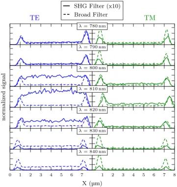
Another evidence of the SHG sensitivity to the dielec-tric contrast is given in Fig. 4, where the intensity profiles are drawn along the NW300 axis for different excitation wavelengths at a fixed detection window (SHG filter). The difference between the TM and TE configurations is detected only when the excitation wavelength is equal to twice the detection wavelength. In the other cases, as
0 1 2 3 4 5 6 7 8 0.4 0.8 1.2 1.6 Y( µm) a 0.4 0.8 1.2 1.6 Y( µm) b 0 1 2 3 4 5 6 7 8 X (µm) 0 2 4 Iph oto (nA ) c TE TM
E
inE
inFIG. 3. SHG maps of NW300 for (a) TE polarization, (b) TM polarization and (c) intensity profiles along the NW axis.
well as for the profiles recorded using the longpass filter (corresponding to the broad PL band induced by third order processes), a totally different behavior is obtained. All profiles except the SHG ones look very similar, are independent of the incident light polarization, with ”hot spots” located at both NW tips.
There are different sources of SHG in centrosymmetric materials.16,20,21These sources are divided between
sur-face local contributions due to the rapid change of the electric field at the interface between the nano-object and its embedding medium and non-local bulk contributions which depend on the gradient of the incident electric field. It is generally assumed that the normal non-linear surface polarization is the main contribution to SHG from gold nanostructures, this contribution being highly sensitive to the shape of the nano-object,22 or proximity to an-other nano-object.23In the case of silicon nanostructures,
the relative weight of surface and bulk contributions is not well-known. Extensive numerical simulations are re-quired to address the SHG mechanism from Si-NWs.
The first conclusion of our work is that far-field SHG microscopy performed on silicon nanowires gives access to the local near-field intensity distribution at the fun-damental frequency, in agreement with similar experi-ments on gold nanorods.13 The comparison of the SHG
maps of Fig. 3 and the results of electrodynamical sim-ulations provided in supplementary information indeed shows that the general aspect, TE and TM polarization dependence and intensity ratio are qualitatively recov-ered in our experiments. (See Supplemental Informa-tion, Section II: Near-field intensity distribution of a sil-icon nanowire)This conclusion is supported by previous study of the photoluminescence (PL) of silicon
nanocrys-TE SHG Filter (x10) Broad Filter λ= 780 nm TM λ= 790 nm λ= 800 nm normalized signal λ= 810 nm λ= 820 nm λ= 830 nm 0 1 2 3 4 5 6 7 X (µm) 1 2 3 4 5 6 7 8 λ= 840 nm
FIG. 4. Intensity profiles along the NW300 axis as function of the excitation wavelength for two different detection windows (SHG filter (solid line) and PL filter (dashed line)), and for both polarization configurations (TE blue, TM green).
tals located in the optical near-field of Si-NWs,8 which
showed that the PL mapping was in good agreement with the computed near-field intensity distribution of the Si-NW.8
At last, it must be noticed that SH detected in our ex-periments can be strongly enhanced in Si-NWs compared to bulk silicon. The values of the SHG yield for different materials excited under the same conditions are summa-rized in Table I. The measured SHG intensities are higher for Si-NWs than for bulk Si and SOQ layer, even more when the SHG signal is renormalized by the area Kspot
of the laser spot that is actually illuminating the Si-NW.
(See Supplemental Information, Section III: Correction factor for the SHG of silicon nanowires and bulk materi-als)This correction is necessary since the minimal laser spot radius (≈ 620 nm for λexc= 810 nm) is much larger
than the Si-NW diameters. The corrected SHG signal of Si-NWs may be two orders of magnitude larger than bulk Si and SOQ layer.
The SHG yield is very different depending on the TM or TE configuration, and on the NW diameter. There-fore, it is interesting to compare the Iphoto/Kspot results
in view of the scattering efficiency at the excitation wave-length, thus addressing another contribution to the SHG yield than surface and dielectric contrast effects. Notice however that we did not take into account the optical absorption, since it is the same for all silicon samples (no resonance around 810 nm for Si-NWs).
4
TABLE I. Comparison of SHG signals. Iphoto/Kspotis the normalized photocurrent (see text). Laser power and wavelength were fixed at 3.15 mW/µm2
and 810 nm, respectively. The scattering efficiency Qscat.at 810 nm is calculated using Mie theory.3
Sample Polarization Position Iphoto (nA) Kspot Iphoto/Kspot(nA) Qscat.
Glass – – 0.015 1 0.015 – Si Bulk – – 0.19 1 0.19 – SOQ – – 0.22 1 0.22 – NW50 TE Tip/Center 0/0 0.073 0/0 0.014 TM Tip/Center 2.5/1.6 34.2/21.9 3.32 NW80 TE Tip/Center 0.30/0.30 0.116 2.6/2.6 0.061 TM Tip/Center 4.8/4.4 41.4/37.9 6.34 NW300 TE Tip/Center 3.3/3.8 0.436 7.6/8.7 0.60 TM Tip/Center 5.6/1.6 12.8/3.7 1.61
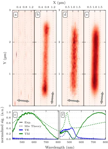
mappings of small diameter NWs, such as NW50, sup-porting only one of these optical resonances (Fig. 5a-c). In that case, the fundamental resonance branch is non-degenerate and only the TM01 mode can be excited.1,3
Thus, a high SHG yield is measured in the TM con-figuration, corresponding to a large scattering efficiency (Qsca= 3.3), while no SHG is detected for
perpendicu-larly polarized incidence, due to the absence of any TE mode (Qsca= 0). The behavior for NW80 (in Fig. 5d-f)
is quite similar to NW50, with a non-degenerate TM01
mode matching the excitation wavelength (810 nm). The higher SHG yield of NW80 in the TM configuration can be attributed to the large scattering efficiency at the ex-citation wavelength, and possibly at the detection wave-length (405 nm). The SH intensity involving local field enhancement factors at both the fundamental and har-monic wavelengths has been reported in the case of gold nanorods.24,25 However, a very weak SHG instead of no
SHG for NW50 can be distinguished in the mapping of the TE configuration (Fig. 5d). This could be related to the value of Qscatat the excitation wavelength for NW80
which is slightly higher than Qscat for NW50 (see
ta-ble I), and again to the presence of a resonance mode at the harmonic wavelength (degenerate TM11-TE01 mode
around 450 nm). As mentioned previously, the influence of optical absorption can be neglected as the absorption efficiency is very weak for all NWs at the fundamental wavelength (even for large diameter Si-NWs above 200 nm where absorption resonances may appear).
In conclusion, we have studied the nonlinear optical response from individual Si-NWs of different diameters. We identified different nonlinear contributions, one of them being second harmonic generation. First, we exploited the SHG, which is highly sensitive to small variations of the local electric field and furthermore boosts the resolution of the SHG mappings of a nanowire, to access to the local electromagnetic field distribution of a Si-NW. Second, we showed that Si-NWs are good candidates for enhanced SHG, thanks to the presence of resonant optical modes. The optimization of the SHG yield could be achieved by adjusting the nanowire
0.4 0.8 1.2 0 1 2 3 Y (µ m) a 0.4 0.8 1.2 b 500 600 700 800 0.0 0.2 0.4 0.6 0.8 1.0 normalized sig. (a.u.) c Exp. Mie Theory TE TM 0.5 1.0 1.5 X (µm) 0 1 2 3 d 0.5 1.0 1.5 e 500 600 700 800 Wavelength (nm) f
FIG. 5. SHG maps for (a) (resp. (d)) TE, and (b) (resp. (e)) TM polarizations in the case of NW50 (resp. NW80). Normalized elastic light scattering spectra compared to Mie theory for (e) NW50, and (f) NW80.
diameter (hence the resonances), for instance to match simultaneously the fundamental and harmonic frequen-cies. This may open a route towards new Si-based nonlinear optical devices.
The authors thank Dr C. Girard (CEMES) for fruitful discussions and Dr F. Fournel (CEA-LETI) for providing the SOQ substrate. The optical set-up was partly funded
under ”Campus Gaston Dupouy” grant. This work was supported by the computing facility center CALMIP un-der grant P12167.
∗
corresponding author : [email protected] 1
L. Cao, P. Fan, A. P. Vasudev, J. S. White, Z. Yu, W. Cai, J. A. Schuller, S. Fan, and M. L. Brongersma, Nanolett. 10, 439 (2010).
2
M. L. Brongersma, Yi Cui, and S. Fan, Nature Mat. 13, 451 (2014).
3 H. Kallel, A. Arbouet, G. BenAssayag, A. Chehaidar, A. Poti´e, B. Salem, T. Baron, and V. Paillard, Phys. Rev. B 86, 085318 (2012).
4 S. M. Wells, I. A. Merkulov, I. I. Kravchenko, N. V. Lavrik, and M. J. Sepaniak, ACS nano 6, 2948 (2012).
5
F. Priolo, T. Gregorkiewicz, M. Galli, and T. F. Krauss, Nature Nanotech. 9, 19 (2014).
6
V. E. Ferry, A. Polman, H. A. Atwater, ACS nano 12, 10055 (2011).
7 P. Albella, R. Alcaraz de la Osa, F. Moreno, and S. A. Maier, ACS photonics 1, 524 (2014).
8
H. Kallel, A. Arbouet, M. Carrada, G. BenAssayag, A. Chehaidar, P. Periwal, T. Baron, P. Normand, and V. Pail-lard, Phys. Rev. B 88, 081302(R) (2013).
9 R. Paniagua-Dom´inguez, G. Grzela, J. G´omez Rivas, and J. A. S´anchez-Gila, Nanoscale 5, 10582 (2013).
10
R. Grange, G. Br¨onstrup, M. Kiometzis, A. Sergeyev, J. Richter, C. Leiterer, W. Fritzsche, C. Gutsche, A. Lysov, W. Prost, F.-J. Tegude, T. Pertsch, A. T¨unnermann, and S. Christiansen, Nanolett. 12, 5412 (2012).
11
R. Sanatinia, S. Anand, and M. Swillo, Nanolett. 14, 5376 (2014).
12
P. Ghenuche, S. Cherukulappurath, T. H. Taminiau, N. F. Van Hulst, and R. Quidant, Phys. Rev. Lett. 101, 116805 (2008).
13
J. Berthelot, G. Bachelier, M. Song, P. Rai, G. Colas des Francs, A. Dereux, and A. Bouhelier, Opt. Express 20, 10498 (2012).
14 R. Salh, Defect related luminescence in silicon dioxide net-work: a review. In Crystalline Silicon - Properties and Uses, S. Basu (Ed.), pp. 135-172. Rijeka: InTech (2011).
15 H. W. K. Tom, T. F. Heinz, and Y. R. Shen, Phys. Rev. Lett. 51, 1983 (1983).
16
S. Cattaneo, and M. Kauranen, Phys. Rev. B 72, 033412 (2005).
17
M. Cazzanelli, F. Bianco, E. Borga, G. Pucker, M. Ghulinyan, E. Degoli, E. Luppi, V. V´eniard, S. Ossicini, D. Modotto, S. Wabnitz, R. Pierobon, and L. Pavesi, Nature Mat. 11, 148 (2012).
18
Raman spectra of Si-NWs do not exhibit any significant strain-induced phonon shift.
19 V. Barzda, R. Cisek, T. L. Spencer, U. Philipose, H. E. Ruda, and A. Shik, Appl. Phys. Lett. 92, 113111 (2008). 20
R. Cisek, V. Barzda, H. E. Ruda, and A. Shik, IEEE J. of selected topics in quantum electronics, 17, 915 (2011). 21
G. Bachelier, J. Butet, I. Russier-Antoine, C. Jonin, E. Benichou, and P.-F. Brevet, Phys. Rev. B 82, 235403 (2010).
22
J. Butet, K. Thyagarajan, and O. J. F. Martin, Nanolett. 13, 1787 (2013).
23
J. Butet, and O. J. F. Martin, ACS nano 8, 4931 (2014). 24
C. Hubert, L. Billot, P.-M. Adam, R. Bachelot, P. Royer, J. Grand, D. Gindre; K. D. Dorkenoo, A. Fort, Appl. Phys. Lett. 90, 181105 (2007).
25
1
Supplemental Materials: Enhanced nonlinear optical response from individual silicon
nanowires
I. NONLINEAR OPTICAL MICROSCOPY EXPERIMENTS
The beam of a mode-locked Ti-sapphire femtosecond-laser covering the 700 nm-1000 nm wavelength range (80 MHz repetition rate, 150 fs pulse duration) is focused through a 50x, 0.8 NA microscope objective. The emitted light is collected in the backscattering geometry using the same microscope.
Spectra at different points of the samples are obtained using a Princeton Instruments IsoPlane 320 spectrometer coupled to a Pixies 400 CCD device. A nano-displacement stage is used to move the sample for 2D mapping (usually steps of 100 nm). In that case, either longpass or bandpass filters and a photomultiplier tube (PMT) are used. The bandpass filter (FBH405, 405 nm, 10 nm FWHM) is used to select the second harmonic generated by λ = 810 nm laser light (the so-called SHG filter in the article). The longpass filter (GG435, starting at 435 nm), or broad filter, is used to measure the nonlinear broad band emission generated by two or more absorbed photons. Finally, a BG39 bandpass filter (360-580 nm) is always added to eliminate any unwanted fundamental light, leaking through the dichroic mirror. The incident polarization is fixed. The TE and TM configurations (polarization perpendicular and parallel to the NW axis, respectively) are obtained by rotating the sample. The incident power density is thus never changed. Except for power dependence measurements, the average power density was fixed at 3.15 mW/µm2.
Interferometric autocorrelation experiments are performed using two coherent pumps.S1 The laser pulse is split in
two beams of equal power, which are time-delayed before being focused on the sample in the same spot through the microscope objective. The average power density for each beam was fixed at 1.35 mW/µm2.
Power dependence measurements are shown in Fig. S1e, where the spectra are given as function of increasing laser power. The log-log inset shows a slope of 2 for the sharp peak’s maximum intensity (SHG), whereas the broad photoluminescence band rises with a slope of 3. For these experiments the fundamental light was 840 nm (harmonic light at 420 nm) to optimize the transmission of the microscope objective and the spectrometer’s detection efficiency. Results were reproducible with increasing and then decreasing power density, as long as keeping the power density below a damage threshold.
0 2 4 6 8 a SHG, TE fit 0 2 4 6 8 b SHG, TM −0.4 −0.2 0.0 0.2 0.4 ∆t (ps) 0 10 20 30 normalized signal (a.u.) c Broad, TE −0.4 −0.2 0.0 0.2 0.4 ∆t (ps) 0 10 20 30 d Broad, TM wavelength (nm) 400 450 500 550 600 avg. pow er(m W) 05 1015 20 signal (a.u.) 0.0 0.2 0.4 0.6 0.8 1.0 10 5 6 7 8 9 20 power (mW) 10−2 10−1 100 signal (a.u.) e n= 2 n= 3
FIG. S1. Interferometric autocorrelation spectra for SHG ((a) and (b)) and broad nonlinear photoluminescence band ((c) and (d)). (e) Nonlinear spectra as function of laser power recorded on the NW tip in TM configuration. Log-log plots showing the power dependence are given in the inset (n = 2 and n = 3 slopes are drawn as a guide for the eye).
To validate the use of filters for SHG mapping, we performed interferometric autocorrelation measurements on the SHG and the broad PL band. The experiments were performed using a fundamental light of 810 nm. Detection was limited to either second harmonic using a FBH405-bandpass filter or to the broad luminescence band using a GG435-longpass filter. Results are shown in Fig. S1a-d.
The measured intensity of the interferometric autocorrelation signal at time delay δ writes: INL(δ) = ∞ Z −∞ [Epulse1(t) + Epulse2(t − δ)] 2 n dt (S1)
with Epulse1,2(t) the electric field of pulse 1,2 at the sample at time t, and n the nonlinear exponent. Setting both
pulses to equal amplitudes A1= A2= A, the ratio of maximum signal (δ = 0) to infinite delay signal is:
R = INL(0) INL(∞) = [2 · A]2 n 2 · |A2|n = 4n 2 (S2)
which gives R = 8 for n = 2, R = 32 for n = 3, ...
The fit to the envelope of the experimental spectra shows that the amplitude is nearly 8 for the spectrum recorded using the SHG filter (Fig. S1(a) and (b)), thus corresponding to second harmonic generation. The amplitude for the large PL band is slightly inferior to 32, in agreement with a third order process (Fig. S1(c) and (d)).
II. NEAR-FIELD INTENSITY DISTRIBUTION OF A SILICON NANOWIRE
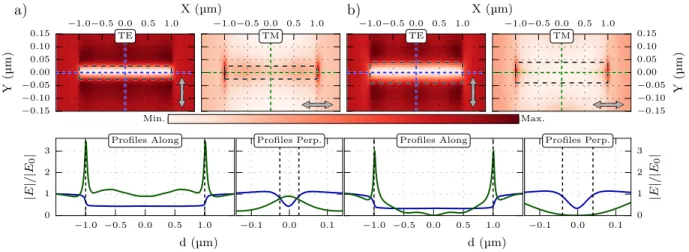
Fig. S3 shows the near-field intensity distribution at 10 nm (one discretization step) below a Si-NW placed in vacuum calculated using the Green Dyadic technique.S2The latter relies on a volume discretization of the system and allows to describe nanostructures of arbitrary morphology. This technique rigorously takes into account the dielectric response of the substrate. Due to excessive computational requirements, it is impossible to perform a simulation of a 300 nm diameter, 6µm long Si nanowire. We limit the nanowire sizes to 2 µm in length and to 50 and 80 nm in diameter, corresponding to the other sizes investigated experimentally. The near-field maps are in qualitative agreement with the SHG maps of Fig. 3 and Fig. 5 of the article. The electric field is strongly enhanced in TM configuration at the NW edges only. It is not or weakly enhanced but homogeneous all along the NW axis in the TE configuration. The absence or weak field enhancement in the TE case is due to the absence of any resonance for the small diameter Si-NWs at the excitation wavelength (810 nm).
−1.0−0.5 0.0 0.5 1.0 −0.15 −0.10 −0.05 0.00 0.05 0.10 0.15 Y (µ m) a) TE −1.0−0.5 0.0 0.5 1.0 X (µm) TM −1.0 −0.5 0.0 0.5 1.0 d (µm) 0 1 2 3 |E |/ |E 0 | Profiles Along −0.1 0.0 0.1 Profiles Perp. −1.0−0.5 0.0 0.5 1.0 b) TE −1.0−0.5 0.0 0.5 1.0 X (µm) −0.15 −0.10 −0.05 0.00 0.05 0.10 0.15 Y (µ m) TM −1.0 −0.5 0.0 0.5 1.0 d (µm) Profiles Along −0.1 0.0 0.1 0 1 2 3 |E |/ |E 0 | Profiles Perp. Min. Max.
FIG. S2. Near-field intensity distribution of a 2µm long Si-NW (diameter of 50 nm (a) and 80 nm (b)) for TE and TM configurations under plane wave excitation at 810 nm. Lower figures : normalized intensity distribution drawn along the dotted blue and green lines in the upper images. In each case, profiles parallel and perpendicular to the NW axis are given.
III. CORRECTION FACTOR FOR THE SHG OF SILICON NANOWIRES AND BULK MATERIALS
In our experimental conditions, the diffraction limited minimal spot radius rspot≈ 0.61λ/NA ≈ 620 nm (for λ =
810 nm) is always larger than the Si-NW diameter. The illuminated fraction of the nanowire is estimated by a factor Kspot =
SonNW
Sspot
3 with the intersection of spot and NW surface SonNW= dNW· 2rspot/
√
2, and Sspot= π(rspot/
√
2)2. The spot area is taking into account the 2nd order of the nonlinear process (the factor 1/√2 is due to the squared Gaussian beam
width).
The photocurrent is divided by Kspot to obtain the normalized SHG yield, allowing the comparison of nanowires
to bulk samples. The absorption efficiency at the excitation wavelength is the same for all silicon samples. Results are shown in Table II of the article.
nanowire laser spot 2rspot dNW Sspot SonNW
FIG. S3. Sketch showing the illuminated fraction of a nanowire by a circular laser spot.
∗
corresponding author : [email protected]
[S1] A. Monmayrant, S. Weber, and B. Chatel, J. Phys. B: At. Mol. Opt. Phys. 43, 103001 (2010). [S2] C. Girard, Reports on Progress in Physics 68, 1883 (2005).