The Design and Construction
of a Data Path Chip Set for a
Fault Tolerant Parallel Processor
by
Charles E. Sakamaki
Submitted to theDepartment of Electrical Engineering and Computer Science in partial fufillment of the requirements for the degrees of
Master of Science in
Electrical Engineering and Computer Science and
Bachelor of Science in Electrical Science and Engineering
at the
Massachusetts Institute of Technology February 1991
© Charles E. Sakamaki, 1991
The author hereby grants to M.I.T. permission to reproduce and to distribute copies of this thesis in whole or in part. Signature of Author
Department of Electrical Engineering and Computer Science February 1, 1991 Certified by Chomas F. Knight, Jr. Thesis Supervisor Certified by Richard E. Harper Charles S§ark Drapr ,4abbratory
Accepted by. ,I
'Arthur C. Smith Chairman, Departmental Committee on Graduate Students
ARCHIVEb
MASSAC•iUSETS INSTITUTE OF TECHNOLOGY
J UL
2
4 1991
The Design and Construction
of a Data Path Chip Set for a
Fault Tolerant Parallel Processor
by
Charles E. Sakamaki
Submitted to the Department of Electrical Engineering and Computer Science on February 6, 1991 in partial fulfillment of the requirements for the degrees of
Master of Science and
Bachelor of Science
Abstract
Reliability of a computer architecture may be increased through fault tolerance. However, fault tolerance is achieved at a price of decreased throughput. The Fault Tolerant Parallel Processor at the Charles Stark Draper Laboratory maintains high levels of reliability and throughput by combining technologies of fault tolerance and parallel processing. The architecture is based on a Network Element (NE), which performs the functions of fault tolerance and parallel processing. A design for two field programmable gate arrays (FPGAs) is proposed herein which will replace much of the NE and perform the communication, synchronization, and redundancy management functions within the NE. This will yield increased reliability, reduced size, and reduced power dissipation. These FPGAs will be integrated with the next implementation of the Fault Tolerant Parallel Processor.
Thesis Supervisor:
Acknowledgments
This work would not have been possible without the expertise and support of the staff of the Fault Tolerant Systems Division of the Charles Stark Draper Laboratory. In particular, special thanks must be extended to Richard Harper, Bryan Butler, Martin McKinney, Mark Busa, Paul Mukai, and Eric Damon. I would also like to thank my thesis advisor Tom Knight for his support and direction, and finally my family and friends for their support and encouragement
This work was done at the Charles Stark Draper Laboratory under an internal research and development grant.
Publication of this report does not constitute approval by the Draper Laboratory of the findings or conclusions contained herein. It is published for the exchange and stimulation of ideas.
I hereby assign my copyright of this thesis to the Charles Stark Draper Laboratory, Inc.,
Cambridge, Massachusetts.
Charles E. Sakamaki
Charles Stark Draper Laboratory hereby grants permission to the Massachusetts Institute of Technology to reproduce and to distribute this thesis in whole or in part.
Table of Contents
Table of Contents
1 Introduction...13 1.1 Problem Statement...13 1.2 O bjective...14 1.3 Approach...142 Fault Tolerance Fundamentals...15
2.1 Fault Tolerance Requirements...15
2.2 AdHocApproach...16
2.3 Byzantine Resilience Approach ... 16
3 Byzantine Resilience...17
3.1 Solution to the Byzantine Generals Problem...17
3.2 The One-Byzantine Resilient System...18
3.3 The Two-Byzantine Resilient System...22
4 Fault Tolerant Computers ... 23
4.1 The AIPS Fault Tolerant Computer ... 24
4.2 The C1 Fault Tolerant Parallel Processor...25
4.3 The Multicomputer Architecture for Fault Tolerance...32
4.4 The Network Element Based Fault Tolerant Processor...33
4.5 The Software Implemented Fault Tolerance Computer ... 35
5 The C3 Fault Tolerant Parallel Processor...37
5.1 C3FTPPHardware...38
5.2 C3 FTPP Exchange Protocol...41
5.3 The Data Path Chip Set ... 54
6 C3 FTPP Data Path Chip Set Hardware...59
6.1 Types of Design...59
6.2 Data Path Chip Set Technology...60
Table of Contents
7 The Fault Tolerant Clock Chip ... 67
7.1 Asynchronous Control...69
7.2 Debug Wrap Register ... 70
7.3 Fault Tolerant Clock...71
7.3.1 Bane State Machine...72
7.3.2 Bound Generator ... 74
7.3.3 Mask Latch ... 76
7.3.4 Mid Data Transfer ... 77
7.3.5 My State Machine...78
7.3.6 Packet Latch and Counter ... 80
7.3.7 Presence Accumulator...82
7.3.8 Propagation Delay Latch and Counter...83
7.3.9 Synchronization Feedback...84
7.4 Latch Decode -FTC...85
7.5 Link Error Accumulator...86
7.6 Synchronous Control...87
7.7 VDATBusDriver...89
8 The Voter Chip...91
8.1 Latch Decode- Voter...91
8.2 Mask Register...93
8.3 Syndrome Accumulator...98
8.4 Voter...99
8.5 VDATBusDriver...102
9 Simulation and Testing...103
9.1 Timing Model...104
9.2 The Fault Tolerant Clock Chip...106
9.2.1 Asynchronous Control...106
9.2.2 Debug Wrap Register ... 107
9.2.3 Fault Tolerant Clock...108
9.2.4 Latch Decode -FTC...114
9.2.5 Link Error Accumulator...115
9.2.6 Synchronous Control ... 116
9.2.7 VDAT Bus Driver ... 117
9.2.8 Overall FTC FPGA Simulation...118
9.3 The Voter Chip...119
9.3.1
Latch Decode - Voter...119
9.3.2
Mask Register...120
9.3.3
Syndrome Accumulator...121
9.3.4 Voter ...
121
9.3.5 VDAT Bus Driver ... 122
9.3.6 Overall Voter FPGA Simulation...123
-ate 01 OItontenis
10 Conclusions and Recommendations...125
APPENDIX A - FTC Chip Schematics FTC Chip...127
Asynchronous Control...128
Debug Wrap Register...129
Fault Tolerant Clock...130
Bane State Machine...131
Bound Generator...132
Set Reset Latch...133
Mask Register...134
Absolute to Relative Decoder...135
5 to 1 Multiplexer...136
Mid Data Transfer...137
My State Machine...138
Packet Latch and Counter...139
Down Counter...140
Presence Accumulator...141
Propagation Delay Latch and Counter...142
Latch Decode - FTC...143
Link Error Accumulator...144
Synchronous Control...145
Bus Driver...146
APPENDIX B - Voter Chip Schematics Voter Chip...147
Latch Decode - Voter...148
Mask Register...149
NE Mask Latch...150
PE Mask Latch...151
Source Mask Latch ... 152
Absolute to Relative Decoder...153
5 to 1 Multiplexer ... 154
Syndrome Accumulator...155
Voter (1 bit) ... 156
Voter Pipeline Register ... 157
Voter Error Generator...158
Bus Driver...159
APPENDIX C - FTC Chip Simulation...161
APPENDIX D - Voter Chip Simulation ... 162
APPENDIX E - FTC Chip Pinouts ... 163
APPENDIX F - Voter Chip Pinouts...164
List of Figures
3.1 Lieutenant 2 is a Traitor...19
3.2 Commander is a Traitor...19
3.3 Lieutenant 3 is a Traitor ... 20
3.4 Commander is a Traitor ... 21
3.5 A One-Byzantine Resilient System ... 21
3.6 A Two-Byzantine Resilient System...22
4.1 AIPS Fault Tolerant Processor Architecture...24
4.2 The C1 Fault Tolerant Parallel Processor Architecture...26
4.3 Block Diagram of the C1 FTPP Network Element ... 27
4.4 Class 1 Message Exchange ... 29
4.5 Class 2 Message Exchange (Round 1)...30
4.6 Class 2 Message Exchange (Round 2) ... 31
4.7 The Multicomputer Architecture for Fault Tolerance ... 32
4.8 The NEFTP Architecture...34
5.1 C3 FTPP Architecture...37
5.2 Block Diagram of the C3 FTPP Network Element ... 39
5.3 Basic C3 FTPP Network Element Cycle...41
5.4 C3 FTPP SERP Exchange Timing ... 42
5.5 C3 FTPP SERP Phase One...43
5.6 C3 FTPP SERP Phase A ... 44
5.7 C3 FTPP SERP Phase B ... 45
5.8 C3 FTPP SERP Phase C ... 46
5.9 C3 FTPP SERP Phase D ... 47
5.10 C3 FTPP SERP Phase E...48
5.11 C3 FTPP Class 1 Message Exchange...49
5.12 C3 FTPP Class 1 Exchange Timing...50
5.13 C3 FTPP Class 2 Message Exchange (Round 1)...51
5.14 C3 FTPP Class 2 Message Exchange (Round 2)...52
5.15 C3 FTPP Class 2 Exchange From NE A Timing ... 53
5.16 Block Diagram of C3 FTPP Data Path Chip Set...54
5.17 Equivalent of Data Path Chip Set Using PALs and ITL logic ... 55
5.18 Data Path Chip Set Using Altera FPGAs ... 55
List of Figures
6.1 PLD Cost Effectiveness...61
6.2 EPM5128 Block Diagram...62
6.3 Altera Macrocell Block Diagram ... 63
6.4 Typical EPM5128 Power Consumption ... 64
6.5 NEFTP NE Chip Equivalent ... 65
7.1 Block Diagram of FTC Chip ... 68
7.2 Debug Wrap Register Circuitry ... 70
7.3 FTC Block Diagram...72
7.4 State Diagram for Bane State Machine ... 73
7.5 Bound Generation Schematics ... 75
7.6 MEDBOUND Generation...75
7.7 Absolute to Relative Conversion...76
7.8 Mask Latch Circuitry ... 77
7.9 Mid Data Transfer Logic ... 78
7.10 State Diagram for My State Machine ... 79
7.11 Packet Latch Schematics...80
7.12 Four-Bit Down Counter...81
7.13 Presence Accumulator Schematics...82
7.14 Propagation Delay Latch Schematics...83
7.15 Synchronization Feedback Schematics...84
7.16 Link Error Accumulator Schematics...87
7.17 SHOUT/ Generation...88
7.18 VDAT Bus Driver Circuitry ... 89
8.1 Block Diagram of Voter Chip ... 92
8.2 Block Diagram of Mask Register ... 94
8.3 NE Mask Register Circuitry ... 95
8.4 PE Mask Register Circuitry...96
8.5 Absolute to Relative Converter...97
8.6 Latching Syndrome Errors on the VDAT Bus...98
8.7 Voter BlockDiagram...99
8.8 Voter Pipeline Register...100
8.9 Voter Error Detection Logic ... 101
9.1 EPM5128 Timing Model...104
9.2 Asynchronous Control Simulation for Normal Operation ... 106
9.3 Asynchronous Control Simulation in Debug Mode...107
9.4 Debug Wrap Register Simulation...108
9.5 Bane State Machine Simulation for No Propagation Delay ... 109
9.6 Bane State Machine Simulation for a Propagation Delay of Four...109
9.7 Bound Generator Simulation...110
9.8 FTC Mask Latch Simulation...110
9.9 Mid Data Transfer Simulation ... 111
9.10 FTC My State Machine Simulation (Ahead)...111
9.11 FTC My State Machine Simulation (Normal) ... 112
9.12 FTC My State Machine Simulation (Behind)...112
9.13 FTC Packet Latch and Counter Simulation...113
9.14 Presence Accumulator Simulation ... 113
9.15 FTC Propagation Delay Latch and Counter Simulation...114
9.16 FTC Latch Decode Simulation ... 115
9.17 Link Error Accumulator Simulation ... 116
9.18 Synchronous Control Simulation...116
9.19 FTC VDAT Bus Driver Simulation...117
9.20 Voter Latch Decode Simulation ... 119
9.21 Mask Register Simulation...120
9.22 Syndrome Accumulator Simulation...121
9.23 Voter Simulation...122
9.24 FTC VDAT Bus Driver Simulation...122
List of Tables
3.1 Requirements for the Byzantine Generals Problem Solution...18
7.1 Asynchronous Control Exchange Modes...69
7.2 Bane State Machine State Equations...74
7.3 VDAT NE Mask Assignments ... 76
7.4 My State Machine State Equations...80
7.5 Presence Accumulator Output Bits...82
7.6 Synchronization Feedback Signals ... 84
7.7 FTC Latch Decode Signals ... 85
7.8 NE Identification Signals...85
7.9 Link Error Accumulator Output Bits...86
7.10 Exchange Types Indicated by NEFUNC ... 87
7.11 Reflecting FIFO Absolute Decoding...88
7.12 Synchronous Control Equations...89
8.1 Voter Latch Decode Signals ... 91
8.2 NE Identification Signals...93
8.3 Mask Register MASKSEL Outputs...93
8.4 VDAT NE Mask Assignments ... 95
8.5 VDAT PE Mask Assignments...96
8.6 Exchange Types and Mask Generation...97
8.7 Syndrome Accumulator Error Format...98
8.8 Truth Table for Non-Quintiplex Voting ... 100
Chapter 1
Introduction
1.1 Problem Statement
The requirement of ultra-reliable computing has led to increasing research in the field of fault tolerant computing. Life critical and mission critical computing systems of the future will have performance and reliability requirements that the current fault tolerant computing systems cannot meet. These systems may be used in the decision-making processes of autonomous mechanisms, which may be used for both military and commercial purposes. An example of a military purpose would be a system to monitor incoming enemy missiles and destroy them when necessary. An example of a commercial purpose would be an automated air traffic controller.
Several fault tolerant computing systems have been designed according to the rules of Byzantine Resilience, such as the Fault Tolerant Multiprocessor (FTMP) [AH78], designed by the Charles Stark Draper Laboratory, and the Software Implemented Fault Tolerance (SIFT) Computer [JG84, JHW78, RWB86], designed by SRI International. However, the SIFT Computer proved inadequate for real-time operation due to the overhead resulting from the implementation of fault tolerance. The AIPS Fault Tolerant Computer (AIPS FTP) [AIPS84], designed by the Charles Stark Draper Laboratory, and the Network Element Based Fault Tolerant Processor (NEFTP) [TAA88], designed by the Charles Stark Draper Laboratory are more recent designs which can meet the performance requirements for real-time operations. The Charles Stark Draper Laboratory is in the process of designing a Cluster Three Fault Tolerant Parallel Processor (C3 FTPP), which surpasses previous fault tolerant systems regarding performance issues by combining properties of fault tolerance and parallel processing. Fault tolerance is necessary for high reliability and parallel processing enhances performance. The C3 FTPP requires a mechanism to provide fault detection and correction, synchronization, and inter-communication in a manner that is compact and reliable.
1.2 Objective
The primary objective of this thesis is to design and develop two field programmable gate arrays (FPGAs) which will be used for error detection/correction, synchronization, and communication purposes in the C3 FTPP. These FPGAs are named the Fault Tolerant Clock (FTC) FPGA and Voter FPGA, collectively known as the Data Path Chip Set. The FTC FPGA will handle the Network Elemv-nt (NE) synchronization and inter-NE communication. The Voter FPGA will handle the error detection/correction. The FPGAs provide compactness, reliability, and low power dissipation for the C3 FTPP design. They provide a significant reduction in physical size over previous designs. The two sixty-eight pin FPGAs support the circuit equivalent of over forty TTL-type chip packages. Numerous design improvements result in increased reliability. CMOS FPGA technology allows for low power dissipation within the FPGAs, which also increases reliability. A design for these FPGAs is developed and fabricated.
1.3 Approach
This study begins with the discussion of some of the fundamentals of fault tolerant processing, in particular, the Byzantine Resilience approach. Several existing fault tolerant computers are then discussed, including the design of the C3 FTPP. The FPGA hardware is examined and the functional blocks for each FPGA are designed. The FPGAs are
Chapter 2 -Fault Tolerance Fundamentals
Chapter 2
Fault Tolerance Fundamentals
This chapter discusses some of the fundamentals of fault tolerance. The major motivation for fault tolerance is the need for ultra-reliable computing. As the demand for automated processes increases, those that are mission-critical and/or life-critical need ultra-reliable computing processes. For instance, a mission-critical operation might involve an unmanned spaceflight to another planet while a critical system might operate the life-support system of a space colony. Fault tolerant computing, as its name suggests, is computing that is able to tolerate faults in such a manner that errors can be detected and corrected prior to propagation throughout the system. Although no system can be 100% error-proof, a fault tolerant system can come close. In today's computer systems, fault tolerance is achieved through the use of redundancy. This redundancy can be done in either hardware or software, or both. An example of software redundancy would include multiple execution and comparison of the same software routines. Multiple processors executing the same software, or the same process in different manners is an example of hardware redundancy.
2.1 Fault Tolerance Requirements
Two key factors in comparing the fault tolerance of different computer architectures are performance and reliability. Performance is roughly measured by the throughput in millions of instructions per second (MIPS), while reliability can be measured as the probability of failure per hour. The throughput requirement on a fault tolerant system depends on the system's function. Most of today's real-time systems have throughput requirements ranging from one to ten MIPS. However, it is conceivable that a future system, such as an autonomous space mission, may have a throughput requirement of 100 MIPS. Typically, the allowable failure probabilities range from 10-4 to 10-6 per hour for
mission-critical functions and 10-6 to 10-10 per hour for vehicle-critical and crew safety functions [JJD88].
There are two basic approaches to fault tolerance, the ad hoc approach and the Byzantine Resilience approach.
Chapter 2 -Fault Tolerance Fundamentals
2.2 Ad Hoc Approach
The ad hoc approach provides fault tolerance for only those modes that are predicted to be likely to occur. This approach is taken in many commercial computers to provide minimal hardware redundancy. In the ad hoc approach, the probabilities of certain failure modes are estimated. Hardware is then designed to tolerate those modes judged to have a sufficiently high probability of occurrence. For instance, a system that operates in an area with faulty power lines may be designed with a backup power supply. Another example would be a data storage/retrieval system that stores multiple copies of data and uses checksums to retrieve correct data.
The ad-hoc approach is inadequate for ultra-reliable computing due to the fact that only the likely failure modes are tolerated, and because human assumptions can be unreliable. Even if the likely failure modes were completely tolerated, which itself is unlikely, the probability of failure is still the sum of the probabilities of all unlikely failure modes. For instance, the system with a backup power supply could easily be defeated by a faulty backup supply or any flaws the system itself has. The data storage/retrieval system could easily be defeated by a checksum that randomly matches corrupt data, or a faulty read/write mechanism.
2.3
Byzantine Resilience Approach
The Byzantine Resilience approach provides tolerance for all failure modes, including malicious failures, which are the worst possible failures that can occur. This approach is taken by several academic and research organizations. Although the probability of malicious failures cannot be determined, they must have a likelihood of less than 10-6 per hour to allow non-Byzantine resilient architectures to even have a chance of meeting the reliability requirements discussed in Section 2.1 The Byzantine Resilience approach is argued to yield much more reliable processes than the ad hoc approach since all failure modes are covered, not only those that are predicted.
The hardware cost of Byzantine resilient system is high, but is argued to be the only practical approach to ultra-reliable computing. The Byzantine Resilience approach is also much more beneficial than the ad-hoc approach since failure modes do not need to be estimated beforehand, thus eliminating the chance of error in human assumptions.
Chapter 3 -Byzantine Resilience
Chapter 3
Byzantine Resilience
Byzantine Resilience is derived from the consensus problem known as the Byzantine Generals Problem. As said in the previous chapter, it is the only practical approach to ultra-reliable computing. The Byzantine Generals Problem is summarized as follows. We imagine that several divisions of the Byzantine army, each commanded by its own general, are camped around an enemy city. The generals can only communicate with one another by messenger. After observing the enemy, the generals must decide upon a common action. However, some of the generals may be traitors, trying to prevent the loyal generals from reaching an agreement [LL82]. The generals must decide on whether to attack or retreat. The problem is to derive a protocol to ensure that all loyal generals agree on a common battle plan, obeying the commanding general whenever he is a loyal general.
The generals in the Byzantine Generals Problem represent processors in a computing system. Traitors represent processors that have malicious failures. The agreement on a common battle plan represents non-faulty processors agreeing on input data. By applying the solution to the Byzantine Generals Problem to a computer system we can develop a computing system that is operational even in the presence of malicious processor failures. This approach is used by the C3 FTPP, among others, to provide ultra-reliability. The communication process used by the Fault Tolerant Clock (FTC) FPGA and the voting process used by the Voter FPGA designed in this thesis is derived from the solution to the Byzantine Generals Problem.
3.1 Solution to the Byzantine Generals Problem
For a given number of traitorous generals, the solution to the Byzantine Generals Problem lies in the number of generals through which messages must be relayed, and to whom each general should relay the message. This solution guarantees that each loyal general will agree on a common battle plan, obeying the commanding general whenever he is a loyal general. Assuming deterministic unauthenticated protocols, a proven solution to the Byzantine Generals problem in the presence of f traitors (or f simultaneous faults) must meet the requirements shown in Table 3.1.
Chapter 3 -Byzantine Resilience
1. There must be at least 3f + 1 participants [LL82].
2. Each participant must be connected to at least 2f + 1 other participants through unique communication paths [DD82].
3. The protocol must consist of a minimum of f + 1 rounds of communication exchange among the participants to allow for the single
sourcing of information [MJF82].
4. The participants must be synchronized to within a known finite skew [DD84-2].
Table 3.1 -Requirements for the Byzantine Generals Problem Solution
A system which meets the requirements shown in Table 3.1 is known to be f-fault Byzantine resilient. For example, a One-Byzantine resilient system must comprise at least four participants, each uniquely interconnected. It uses a two-round communication exchange, with each round of communication occurring during the same approximate time. A Two-Byzantine resilient system must comprise at least seven participants, each connected to at least five other participants. It uses a three-round communication exchange, with each round of communication occurring during the same approximate time.
3.2 The One-Byzantine Resilient System
The One-Byzantine resilient system must comprise four participants. This requirement can be depicted by showing that three participants do not allow for Byzantine fault tolerance.
Consider the case in which there are three participants, one commanding general and two lieutenants, each being able to relay the message of "attack" or "retreat". In the first scenario, Lieutenant 2 is a traitor, as in Figure 3.1. The Commander is loyal and sends the "attack" command to the two lieutenants. Lieutenant 2 then tells Lieutenant 1 that the Commander said to "retreat", since he is a traitor. Lieutenant 1 now cannot figure out what decision to make, since there is is conflicting data and a majority consensus cannot be met. [LL82]
Chapter 3 -Byzantine Resilience
COMMANDER
0 "he said 'retreat'
"he said 'attack'"
LIEUTENANT 1 LIEUTENANT 2
Figure 3.1 -Lieutenant 2 is a Traitor
In the second scenario, the Commander is a traitor, as in Figure 3.2. Since he is a traitor, the Commander sends the "attack" command to Lieutenant 1 and the "retreat" command to Lieutenant 2. Lieutenant 2 then tells Lieutenant 1 that the Commander said to "retreat". Lieutenant 1 cannot figure out what decision to make, since the information he has received is the same as in the first scenario. [LL82]
7 ck" COMMANDER
S"he said 'retreat' "he said 'attack'"
LIEUTENANT 1 LIEUTENANT 2
Figure 3.2 -Commander is a Traitor
Sck"
"attack"
r9??
Chapter 3 -Byzantine Resilience
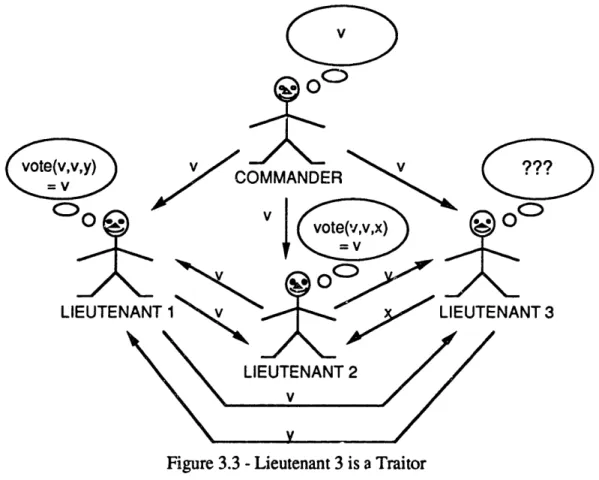
With four participants, however, Byzantine resilience can be achieved even though there is one traitor. In the first scenario, Lieutenant 3 is a traitor, as indicated in Figure 3.3. The Commander is loyal and sends the message v to the three lieutenants, where v can mean either "attack" or "retreat". Lieutenants 1 and 2 then send the message v to the other Lieutenants, while the traitorous Lieutenant 3 sends a message y to Lieutenant 1 and a message x to Lieutenant 2. Lieutenants 1 and 2 can now do a majority vote on the orders received and carry out the message v. [LL82]
ccm
Figure 3.3 -Lieutenant 3 is a Traitor
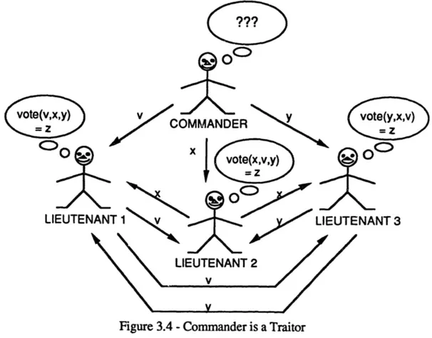
In the second scenario, the Commander is a traitor, as indicated in Figure 3.4. The Commander sends the messages v, x, and y to Lieutenants 1, 2, and 3, respectively. The loyal Lieutenants, then relay the message to the other two Lieutenants so each Lieutenant receives one of each message. The Lieutenants now do a majority vote on the orders received and thus all receive the same message (the majority vote of v, x, and y), which we will call z. In either scenario, the loyal generals can determine which one is traitorous by comparing the majority vote of the orders with the ones they received. [LL82]
Chapter 3 - Byzantine Resilience
cc§3
Figure 3.4 -Commander is a Traitor
So for single sourcing of data, we can create a One-Byzantine resilient system with four participants. A One-Byzantine resilient system consists of at least four Fault Containment Regions (FCRs). A One-Byzantine resilient system with four FCRs is shown in Figure 3.5.
Chapter 3 -Byzantine Resilience
Note that if there are at least three FCRs sourcing the same data in our four FCR system, only one round of communication needs to take place since a simple majority vote of incoming data may be used.
3.3
The Two-Byzantine Resilient System
For single sourcing of data, a Two-Byzantine resilient system must comprise at least seven FCRs, each connected to at least five other FCRs. It uses a three-round communication exchange, with each round of communication occurring during the same approximate time. A Two-Byzantine resilient system consisting of seven FCRs is shown in Figure 3.6.
Figure 3.6 -A Two-Byzantine Resilient System
Note that if there are at least five FCRs sourcing the same data in our seven FCR system, only one round of communication needs to take place since a simple majority vote of incoming data may be used.
Chapter 4 -Fault Tolerant Computers
Chapter 4
Fault Tolerant Computers
There have been several architectures developed which satisfy the requirements for a One-Fault Byzantine resilient system. Among those discussed in this chapter are:
* The Software Implemented Fault Tolerance Computer (SIFT) * The AIPS Fault Tolerant Computer (AIPS FTP)
* The Multicomputer Architecture for Fault Tolerance (MAFR) * The Fault Tolerant Parallel Processor (FTPP)
o The Network Element Based Fault Tolerant Processor (NEFTP)
As the solution in Section 3.1 suggests, a One-Fault Byzantine resilient system must fulfill the following requirements.
1. There must be at least four participants [LL82].
2. Each participant must be connected to at least three other participants through unique communication paths [DD82].
3. The protocol must consist of a minimum of two rounds of communication exchange among the participants to allow for the single
sourcing of information [MJF82].
4. The participants must be synchronized to within a known finite skew [DD84-2].
For simplicity of reference purposes, we will refer to requirement one as the processor
number requirement. Requirement two will be referred to as the connectivity requirement.
Requirement three will be referred to as the communication requirement. Finally, requirement four will be referred to as the synchronization requirement.
Chapter 4 -Fault Tolerant Computers
4.1 The AIPS Fault Tolerant Computer (AIPS FTP)
The AIPS Fault Tolerant Processor (AIPS FTP) [AIPS84] was developed at the Charles Stark Draper Laboratory, Inc. It consists of three processors and three interstages which act as Fault Containment Regions (FCRs) connected as shown in Figure 4.1. The interstages are simple data routers that forward the input to each of the processors. The processors are identical processors executing the same software. They resolve the input data by a 3-way, bit-for-bit majority voter circuit.
Synchronization is achieved through a clock signal called the Fault Tolerant Clock
(FTC). This is employed by a digital phase lock loop circuit in each processor to lock in
phase the FTC signal. The local FTC (LFTC) is approximately an 888 kHz clock signal. Each processor sends its respective LFTC to the interstages, which in turn relay the signals back to the processors. The processors generate FTC by selecting the median value of the three input signals, which should be the same for all processors as long as the interconnection skews between the processors and interstages are the same. All of the processors receive the same number of processor clock (SYSCLK) ticks during the FTC cycle.
Chapter 4 -Fault Tolerant Computers
The three processors of the AIPS FTP are each participants in the Byzantine Generals problem. The interstages act as the fourth participant, fulfilling the participant number requirement for Byzantine resilience. The connectivity requirement is fulfilled by the fact that each processor is connected to all of the interstages, and the interstages are all connected to each processor. Two rounds of exchange take place during the input consistency algorithm. In the first round, the processors forward their respective output data to each of the interstages. In the second round, the interstages forward the data they have received to each processor. These two rounds of communication fulfill the communication requirement for Byzantine resilience. Synchronization is achieved through the Fault Tolerant Clock as previously mentioned. The post-synchronization skew is held to within 125 ns, fulfilling the synchronization requirement.
4.2 The C1 Fault Tolerant Parallel Processor (FTPP)
The Cluster One (C1) Fault Tolerant Parallel Processor (FTPP) [JJD88, REH85, REH87-2] is a computer developed at the Charles Stark Draper Laboratory, Inc., which combines the principles of Byzantine resilience with parallel processing.
The Cl FTPP is grouped into at least four Fault Containment Regions (FCRs), each consisting of four Processing Elements (PEs) and a Network Element (NE) arranged
as in Figure 4.2. Each FCR in the FTPP is physically isolated, electrically isolated (including separate power supplies), and clocked independently. The PEs are off-the-shelf, commercial processor boards that are VME compatible. The C1 FTPP at the Draper Laboratory uses 12.5 MHz versions of the Motorola 68020 VME boards as PEs.
Chapter 4 -Fault Tolerant Computers
FCR A
FCR C
Figure 4.2 -The C1 Fault Tolerant Parallel Processor Architecture
The NE is the heart of the FTPP and performs the communication, voting, and synchronization functions of the system. The NE can be divided into six functional blocks:
* The PE/NE Interface * The NE Data Paths
* The Inter-FCR Communication Links * The NE Fault Tolerant Clock
* The NE Scoreboard * The NE Global Controller
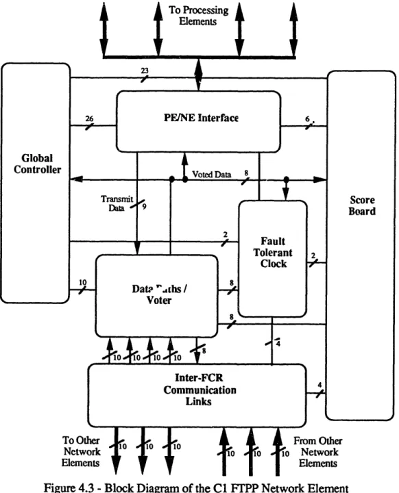
Chapter 4 -Fault Tolerant Computers
The PE/NE Interface provides for the passing of variable size messages between the PE and the NE. The NE Data Paths provides for the handling of one and two round communications exchanges, and the resolution of redundant data copies (majority voting). The Inter-FCR Communication Links provide for passing of data between the FCRs. The NE Fault Tolerant Clock synchronizes an NE with respect to the other NEs. The NE Scoreboard decides which processor exchange, if any, can be performed. Finally, the NE Global Controller is the central micro-controller for the NE. The block diagram of the C1 FTPP is shown in Figure 4.3. To Processing S Elements 26PENE Interface Transmit Data 4 10
r9
tVoted Dhata 8 -4II
L
Fault Tolerant Clock Inter-FCR Communication Links Score BoardTo Other
10
10
Network Elements From Other 10 1 io Network tiElementsFigure 4.3 -Block Diagram of the C1 FTPP Network Element Global Controller Date ".ths / Voter 1 -- -- · I · ·· i V rLCU L I I1L
---II rm---fIm --JA-i ,a --- iI J, -0 4Chapter 4 -Fault Tolerant Computers
The processors of the Cl FTPP are arranged as virtual processors, each consisting of one, three, or four physical processors. A virtual processor consisting of one, three, or four physical processors is called a simplex, triplex, or quadruplex virtual processor, respectively. This provides for different levels of fault tolerance and throughput. Each of the processors in the virtual processing group executes the same code. The members of a virtual processor comprise a Fault Masking Group (FMG). Each of the redundant processors in a virtual processing group reside in a separate FCRs to eliminate single point failures. Communication takes place between the processors by means of the NE.
To maintain synchronization and consistency, the processors exchange messages with each other. Each NE tells the other NEs whether or not its processor needs to exchange information. If all non-faulty processors request the exchange, then the exchange is performed. The data sent by a NE requesting an exchange of information is called an exchange request pattern. Four of these exchanges occur during the first half of this cycle. The series of these four exchanges is called a system exchange request pattern (SERP) exchange.
Once it is determined through a SERP that an exchange is to take place, there are two types of exchanges that can take place. The first type is a Class 1 exchange which is sourced by the members of a triplex or quadruplex virtual processor. During this type of exchange, each FMG member delivers its message to its respective NE, which then relays the message to the other three NEs. Each NE transmits one message and receives three messages. Note that all NEs transmit messages whether the virtual processor is running in
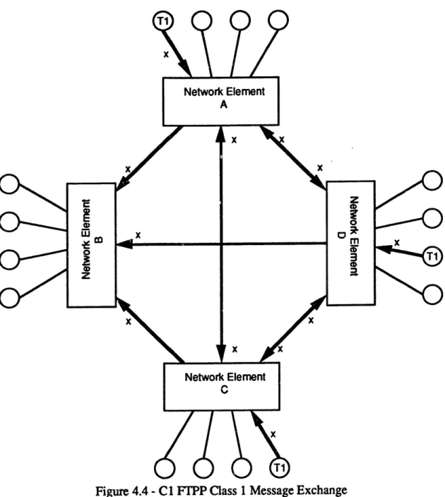
triplex or quadruplex mode. When in triplex mode, the NE not hosting a member of the FMG delivers an empty message to the other NEs. The information received by each NE is then majority voted. Disagreements in the vote are relayed to the processing elements so that Fault Detection Isolation and Reconfiguration (FDIR) software can determine if an element is faulty and reconfigure the system as necessary. The Class 1 message exchange is diagrammed in Figure 4.4.
Chapter 4 -Fault Tolerant Computers
Figure 4.4 -C1 FTPP Class 1 Message Exchange
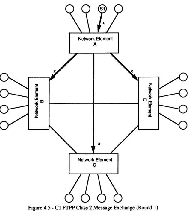
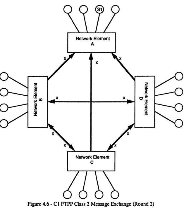
For a simplex virtual processor, a Class 2 message exchange is used. A Class 2 exchange is a two-round exchange. This is identical in concept to the two-round exchange diagrammed in Figures 3.3 and 3.4. In the first round, a member of the FMG single-sources a message to its hosting NE, which then relays this message to the other three NEs. In the second round, each NE reflects the message they received to the other three NEs. Thus, each NE has four copies of the message and can be majority voted. The Class 2 message exchange is diagrammed in Figures 4.5 and 4.6.
Chapter 4 -Fault Tolerant Computers S1 x Network Element A
x
0-oe
zz
0 mq~-X
Network Element CFigure 4.5 - Cl FTPP Class 2 Message Exchange (Round 1)
• m ..- a
I
1-Chapter 4 -Fault Tolerant Computers S1 Network Element A x
0-~~
wz
L--.-. x X X xx
X Network Element CFigure 4.6
-
CI FTPP Class 2 Message Exchange (Round 2)
Since there are four NEs in the Cl FTPP, there are the equivalent of four
participants in the Byzantine Generals Problem. This fulfills the participant number
requirement for Byzantine resilience. Each NE is connected to the other three NEs via a
metallic link. Thus, it meets the connectivity requirement. A Class 2 exchange of data is
used during the simplex mode of operation. It is equivalent to two rounds of
communication. The first round, involves each of the PEs completing a segment of code
and sending its respective output data to the NE. This is similar to the way the commander
issues commands to each of the lieutenants in the Byzantine Generals Problem. The
second round involves the NEs reflecting the data to each of the other NEs and taking a
X ohm
mp
z 0 m!U
~-0
I IChapter 4 -Fault Tolerant Computers
majority vote of all the data. This is similar to the lieutenants' relaying of messages to the
other lieutenants. The triplex and quadruplex also can perform Class 2 exchange modes
which meet the communication requirements for Byzantine resilience. The NEs are
synchronized by the Fault Tolerant Clock mechanism. When data is received outside of a
limited time frame then an error is noted and the local NE's clock is adjusted accordingly.
This method of keeping the NEs within a known skew fulfills the synchronization
requirement. In triplex or quadruplex modes, data is simply majority voted after one round
of exchange. This allows one fault to be detected and corrected during each round of
exchange. Therefore, the Cl FTPP, meets all the requirements for being One-Fault
Byzantine resilient.
4.3 The Multicomputer Architecture for Fault Tolerance
(MAFT)
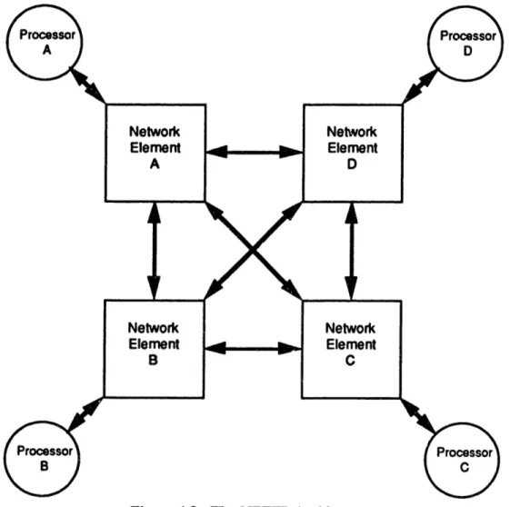
The Multicomputer Architecture for Fault Tolerance (MAFT) [AMF88] attempts to
reduce the overhead of fault tolerance for increased throughput. It consists of four
Operations Controllers (OCs) and four Applications Processors (APs), as shown in Figure
4.7. The OC is the device that handles the fault tolerance. It communicates back and forth
to the AP and to the other OCs. It also performs the data voting, error detection,
synchronization, reconfiguration, and task scheduling for the system.
Figure 4.7 -The Multicomputer Architecture for Fault Tolerance
Chapter 4 - Fault Tolerant Computers
Seeing that there are four processors, the MAFT meets the participant number
requirement for Byzantine resilience. All of the participants are connected to each other
through unique broadcast busses. This meets the connectivity requirement. The two
rounds of communication of the communication requirement take place as follows. In the
first round, all of the the APs send their respective output data to the OC; this is equivalent
to the commander giving his orders. The second round involves the relaying of this data to
the other OCs, representing the intercommunication between the lieutenants. Finally, the
MAFT has a synchronization scheme which synchronizes the participants to within a
known skew (the synchronization requirement). This is done through the exchange of
synchronization messages, which is also sent via the broadcast busses. Thus, the MAFT
fulfills the requirements for One-Fault Byzantine resilience.
4.4
The Network Element Based Fault Tolerant Processor
(NEFTP)
The Network Element Based Fault Tolerant Processor (NEFTP) [TAA88] is
basically a scaled down version of the Cl FTPP (see Section 4.2) also developed at the
Charles Stark Draper Laboratory, Inc. It consists of four Fault Containment Regions
(FCRs), each containing a Processing Element (PE) and a Network Element (NE), as
shown in Figure 4.8. As in the Cl FTPP, the PE is an off-the-shelf, VME compatible
processor board. 20 MHz versions of the Motorola 68030 VME boards are used as PEs.
The NE for the NEFTP is a reduced version of the NE for the Cl FTPP. Since there is
only one PE per NE, the designs of the NE Global Controller and NE Scoreboard are
extremely simplified. The Cl FTPP's NE occupies three VME boards as opposed to one
VME board for NEFTP's NE. Fiber optic links are used instead of metallic links as the Inter-FCR Communication Links. This provides for much better electrical isolation between the FCRs and is less noisy. The NEFTP uses Class 1, Class 2, and SERP message exchanges similar to the C1 FTPP.
Chapter 4 - Fault Tolerant Computers
Figure 4.8 -The NEFTP Architecture
Each of the four FCRs in the NEFTP is equivalent to a participant in the Byzantine Generals Problem. This fulfills the participant number requirement for Byzantine resilience. Each NE is connected to the other three NEs via unique fiber optic links, meeting the connectivity requirement. A Class 2 exchange of data during the simplex mode of operation meets the communication requirement for Byzantine resilience since it is equivalent to two rounds of communication. The NEs are synchronized by the Fault Tolerant Clock mechanism, as in the Cl FTPP, fulfilling the synchronization requirement. In triplex or quadruplex modes, data is majority voted after one round of exchange, thus allowing one fault per exchange. The NEFTP meets all the requirements for being One-Byzantine resilient.
Chapter 4 - Fault Tolerant Computers
4.5
The Software Implemented Fault Tolerance Computer
(SIFT)
The Software Implemented Fault Tolerance Computer (SIFT) [JG84, JHW78, RWB86] is a fault tolerant computer developed by SRI International for NASA to be used in a commercial air transport FBW. The SIFT consists of four to six processors with the processors being fully interconnected. The mechanism for synchronization and fault tolerance of the system is done through software, which leads to serious performance problems.
Having four to six fully interconnected processors, the SIFT fulfills the participant number and connectivity requirements for One-Byzantine resilience. Two rounds of communication take place as follows. First, each processor executes an identical software task (equivalent to the commander's orders). Secondly, each processor relays its output to the other processors for consensus. This meets the communication requirement. To synchronize the system, each processor broadcasts the value of its local clock to the other processors and adjusts its own clock to the other processors, meeting the synchronization requirement. The SIFT, therefore, is a One-Fault Byzantine resilient computer.
Chapter 5 -The C3 Fault Tolerant Parallel Processor
Chapter
5
The C3 Fault Tolerant Parallel Processor
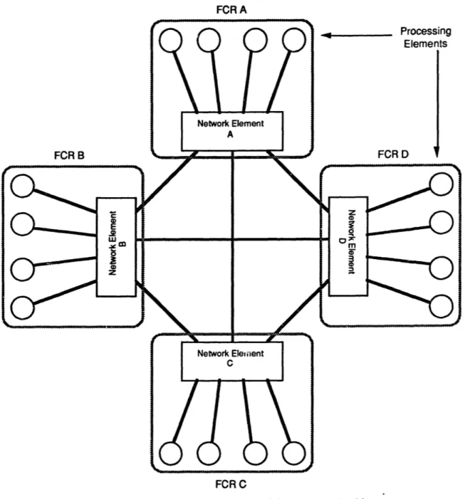
The Cluster Three (C3) version of the Fault Tolerant Parallel Processor (FTPP) is under development at the Charles Stark Draper Laboratory. The C3 FTPP will be similar to the C1 FTPP discussed in Section 4.2, with several enhancements. It will contain up to eight processor elements (PEs) in each network element (NE) instead of the four PEs as in the Cl FTPP. It will also contain up to five NEs instead of four, for a total of forty PEs as opposed to sixteen in the Cl FTPP, which will greatly improve the throughput. The physical size of the NE will be reduced from three full size VME boards to one full size board. The reduced size improves on both the power dissipation and reliability of the Cl FTPP. The architecture for the C3 FTPP is diagrammed in Figure 5.1.
FCR A
FCR C FCR D
Chapter 5 -The C3 Fault Tolerant Parallel Processor
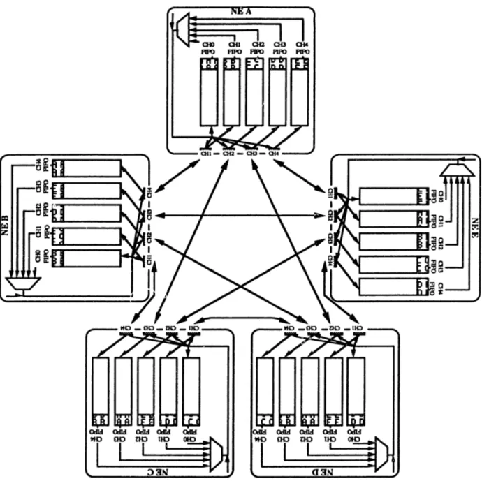
The five network elements are absolutely referenced as NE A, NE B, NE C, NE D,
and NE E, as shown in Figure 5.1, or as 000, 001,010, 011, and 100, respectively, when
represented in binary. Relative addressing is also used when referencing a NE's relative
position. Channel 0 (CH 0) references the local NE itself. CH 1 references the NE
immediately to the right of the local NE as shown in Figure 5.1. Successive channels are
assigned to each NE in counter-clockwise order, so CH 4 references the NE immediately to
the left of the local NE. For example, when NE D represents CH 3 with respect to NE B.
5.1 C3 FTPP Hardware
The NE of the C3 FTPP consists of six major sections, the PE/NE Interface, the
Scoreboard, the Global Controller, the Fault Tolerant Clock, the Data Paths/Voter, and the
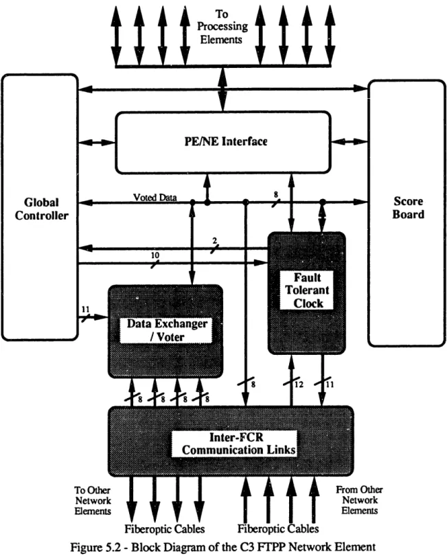
Inter-FCR Communication Links. The block diagram of the NE is shown in Figure 5.2.
Fiber optic links are be used for the Inter-FCR Communication Links instead of metallic
VME links to provide noise reduction and electrical isolation between NEs. The FTC
FPGA designed in this thesis represents the NE Fault Tolerant Clock (FTC) and generates
signals that control the Inter-FCR Communication Links. The Voter FPGA represents
most of the NE Data Paths/Voter. The gray sections of Figure 5.2 represent sections that
the FTC and Voter FPGAs control. Using FPGAs as opposed to standard TTL integrated
circuits results in a reduction in noise due to fewer signal lines, lower power consumption,
and a smaller physical NE size. Since there are twice as many PEs in each FCR and an
additional NE in the C3 FTPP, the PE/NE Interface, NE Scoreboard, and NE Global
Controller sections are also revised.
Chapter 5 -The C3 Fault Tolerant Parallel Processor
Fiberoptic Cables Fiberoptic Cables
Figure 5.2 -Block Diagram of the C3 FTPP Network Element
The Inter-FCR Communication Links consists of one transmitting AMD TAXI chip, which transmits data from the voted data bus, and four receiving AMD TAXI chips, one for each incoming channel. The FTC FPGA synchronizes the local NE with respect to the other NEs by synchronizing itself to the message frames of the other NEs, recording errors when NEs are offsync. It also generates signals that control the Inter-FCR
Chapter 5 -The C3 Fault Tolerant Parallel Processor
Communication Links, recording transmission errors. The Voter FPGA majority votes maskable data from five IDT7202 FIFOs, one for each channel.
The FTC FPGA has an FTC section that handles the synchronization and recording of synchronization errors. This FTC section can be further divided into state machines, latches, and counters. The FTC FPGA has an Asynchronous Control section which controls the loading of the CH1, CH2, CH3, and CH4 FIFOs, which normally occur asynchronously with respect to the local NE's clock. Debug modes are supported, which allow data from an NE to be reflected to itself, so that an NE may be tested individually. A Synchronous Control section in the FTC FPGA controls the shifting out of data from the five FIFOs and shifts data into the CHO FIFO. Transmission errors are recorded by the Link Error Accumulator in the FTC FPGA. The hardware details of the FTC FPGA are discussed in Chapter 7.
The Voter FPGA has a Voter section which majority votes five eight-bit wide maskable channels of data. It generates any errors that result. The Mask Register section of the Voter FPGA generates the various masks that are used by the Voter. The Syndrome Accumulator records errors that occur from the Voter section. The hardware details of the Voter FPGA are discussed in Chapter 8.
The C3 FTPP hardware will support any microprocessor that is VME compatible. Currently, C3 FTPP software will support the 68030 microprocessor from Motorola. However, the 68040 microprocessor from Motorola, the R3000 RISC processor, and the 80386 and 80960 microprocessors from Intel, may be supported at a later date. The processors of the C3 FTPP are arranged as virtual processors, each consisting of one, three, or four physical processors to provide different levels of fault tolerance and throughput. A virtual processor consisting of one, three, or four physical processors is called a simplex, triplex, or quadruplex virtual processor, respectively. The duplex virtual processor is not supported due to the fact that errors can only be detected and not corrected. Note that there is no quintuplex virtual processor even though five network elements do exist. Each of the processors in the virtual processing group executes the same code. The members of a virtual processor are called a virtual group. Each of the redundant processors in a virtual processing group reside in a separate Fault Containment Regions (FCRs) to eliminate single point failures. Communication takes place between the processors in a virtual group by means of the NE. PEs in a virtual group can communicate with other PEs in other virtual groups by means of the NE. Each PE receives identical messages, which are delivered synchronously. By this means, a virtual group can synchronize itself by sending itself a message and awaiting its return. The NEs also synchronize themselves
Chapter 5 -The C3 Fault Tolerant Parallel Processor
upon power up by means of the global controller. The details of the synchronization are discussed in the Fault Tolerant Clock section (Section 7.3).
The C3 FTPP supports dynamic reconfiguration, which allows real-time reconfiguration of the physical processors in a virtual group. This reconfiguration is aided
by the NE Scoreboard, which contains a configuration table (CT) keeping track of the
current configuration of the C3 FTPP. One virtual group, called the reconfiguration authority, is responsible for the updating the configuration table. This group must be a triplex or quadruplex group, assuring one-fault Byzantine resilience.
The C3 FTPP is One-Fault Byzantine resilient. Having five NEs fulfills the participant number requirement. Each NE is inter-connected via fiber optic links, meeting the connectivity requirement. A Class 2 exchange, discussed in the next section, meets the two round communication requirement. The NEs are synchronized by the Fault Tolerant Clock mechanism, fulfilling the synchronization requirement.
5.2
C3 FTPP Exchange Protocol
To maintain synchronization and consistency, the processors exchange messages. Each NE tells the other NEs whether or not its processor needs to exchange information. If all non-faulty processors request the exchange, then the exchange is performed. This cycle is diagrammed in Figure 5.3.
....
E..
... E...
.
PERFORM EXCHANGE
(if
$equested by al
onalty processors) T 0 T SERP T SERP + T EXCHANGE Figure 5.3 - Basic C3 FTPP Network Element CycleThe data sent by a NE requesting an exchange of information is called an exchange request pattern. Five of these exchanges occur during the first half of this cycle. The series of these five exchanges is called a system exchange request pattern (SERP) exchange. The timing of the SERP Exchange is diagrammed in Figure 5.4.
Chapter 5 - The C3 Fault Tolerant Parallel Processor
i
Figure 5.4 - C3 FTPP SERP Exchange Timing
42
I
a B lEa Ii*11
I.'
Ii
A aII
Chapter 5 -The C3 Fault Tolerant Parallel Processor
The first phase of a SERP Exchange involves each NE transmitting its SERP data
to all the other NEs and to itself (CHOFIFO). This is diagrammed in Figure 5.5, which shows the data contained in each NEs FIFOs.
Chapter 5 -The C3 Fault Tolerant Parallel Processor
Phase A of a SERP Exchange involves each NE reflecting the other NEs and to itself. This is diagrammed in Figure 5.6.
NE A FIFO's data to all the
Figure 5.6 -C3 FTPP SERP Phase A WTý A
Chapter 5 -The C3 Fault Tolerant Parallel Processor
Phase B of a SERP Exchange involves each NE reflecting the NE B FIFO's data to all the
other NEs and to itself. This is diagrammed in Figure 5.7.
Chapter 5 -The C3 Fault Tolerant Parallel Processor
Phase C of a SERP Exchange involves each NE reflecting the NE C FIFO's data to all the
other NEs and to itself. This is diagrammed in Figure 5.8.
Chapter 5 -The C3 Fault Tolerant Parallel Processor
Phase D of a SERP Exchange involves each NE reflecting the NE D FIFO's data to all the other NEs and to itself. This is diagrammed in Figure 5.9.
Figure 5.9 -C3 FTPP SERP Phase D
-Chapter 5 -The C3 Fault Tolerant Parallel Processor
Phase E of a SERP Exchange involves each NE reflecting the NE E FIFO's data to all the other NEs and to itself. This is diagrammed in Figure 5.10.
Figure 5.10 - C3 FTPP SERP Phase E
Once it is determined through a SERP that an exchange is to take place, there are two types of exchanges that can take place. The first type is a Class 1 exchange which is sourced by the members of a triplex, or quadruplex virtual processor. During this type of exchange, each member of the ,ritual processor delivers its message to its respective NE, which then relays the message to the other four NEs. Each NE not hosting a member of
-Chapter 5 - The C3 Fault Tolerant Parallel Processor
the virtual processor delivers an empty message to the other NEs. Note that all NEs
transmit messages, so each NE transmits one message and receives four messages.
Messages are transmitted and received by the Inter-FCR Communication Links. The
information received by each NE is then majority voted using the Voter FPGA.
Disagreements in the vote are relayed to the processing elements so that Fault Detection
Isolation and Reconfiguration (FDIR) software can determine if an element is faulty and
reconfigure the system as necessary. The Class 1 message exchange is diagramed in
Figure 5.11. The PEs labeled with a T1 represent members of a triplex virtual processor.
Chapter 5 - The C3 Fault Tolerant Parallel Processor
The Class 1 message exchange timing is diagrammed in Figure 5.12.
All NEs:
)ata Out Transmit Bus Synching 1 Into CHOFIFO -> *
Transmit
Receive ,ReceivingDaalnto FEFOs L .Receivingvin:b
Sync Data
Fiom AH UOter NEs
Vote Vote Data From The FIFOs
Through The Pipelined Registers
Delay x: Propagation delay between NEs ± maximum skew between NEs.
Delay y: The time NE waits from start of data transmission to start of vote (Max NE skew + FIFO write to read time.)
Figure 5.12 -C3 FTPP Class 1 Exchange Timing
For a simplex virtual processor, a Class 2 message exchange is used. A Class 2 exchange is a two-round exchange. In the first round, a member of the FMG single-sources a message to its hosting NE, which then relays this message to the other four NEs. In the second round, each NE reflects the message they received to the other four NEs. Thus, each NE has five copies of the message which is then majority voted. The Class 2 message exchange from NE A is diagramed in Figures 5.13 and 5.14. The PE labeled SI represents a simplex virtual processor.
Chapter 5 -The C3 Fault Tolerant Parallel Processor
Figure 5.13 -C3 FTPP Class 2 Message Exchange (Round 1)
Chapter 5 -The C3 Fault Tolerant Parallel Processor
Figure 5.14 -C3 FTPP Class 2 Message Exchange (Round 2) The Class 2 message exchange from NE A timing is diagrammed in Figure 5.15.
Si
Chapter 5 -The C3 Fault Tolerant Parallel Processor
V:Ii
-
T.
ikA__t t_ U_
Oak-
.
9
Ft
+1I
*II( *3I1
LAU amI
Chapter 5 -The C3 Fault Tolerant Parallel Processor
5.3
The Data Path Chip Set
The C3 FTPP Data Path Chip Set, which includes the FTC FPGA and the Voter
FPGA, performs all the functions of the Fault Tolerant Clock section, generates signals that
control the Inter-FCR Communication Links, and performs most of the functions of the Data Path section of the NE. The only part of the Data Path section not included in the Data Path Chip Set are five IDT7202 2K by 8 FIFOs, since its inclusion would overload the pin and gate capacity of the FPGA. The Inter-FCR Communications Links consists J f four receiving fiber optic data links (FODLs) and one transmitting FODL that drives a one to four splitter, which sends data to each of the other four NEs. Each of the FODLs are driven by an AMD TAXI chip which converts eight bits of parallel data into fiber optic serial data, or vice versa. The block diagram of the Data Path Chip Set is shown in Figure
5.16.
NE INTERFACE (LOCAL NE)
Chapter 5 - The C3 Fault Tolerant Parallel Processor
The Data Path Chip Set allows the physical size of the C3 FTPP to be more compact, to be more reliable, and to have a lower power dissipation as opposed to a design done with PALs and TL chips. If the equivalent of the Data Path Chip Set were to be designed using PALs and TTL chips, the design could be implemented using thirteen 24-pin PALs, seventeen 20-24-pin PALs, five 74AS374 octal latches, two 74LS74 latches, and four 74LS 163 counters. For a size comparison, see Figures 5.17 and 5.18.
Figure 5.17 -Equivalent of Data Path Chip Set Using PALs and TTL logic
Figure 5.18 -Data Path Chip Set Using Altera FPGAs
DEJDO¶ThEJUB
EliIEYJEhUEJEJE
El
El
E~~l
C lElHE
El~l~lVlPlPlF8
Chapter 5 -The C3 Fault Tolerant Parallel Processor The PAL and TTL implementation of the Data Path Chip Set would have a total power dissipation of approximately thirty-three watts, as opposed to approximately three watts using Altera FPGAs.
The failure rate for the FPGA implementation would also be reduced. To get an estimate, we can calculate the estimated reliability by using formulas given in the 1986 Military Handbook for Reliability Prediction of Electronic Equipment. The formulas used in this handbook use the chip gate counts, pin counts, and power dissipations to calculate an estimate of reliability. The PAL and 'ITL implementation of the Data Path Chip Set was calculated to have a reliability of 37.5 failures per one-million hours. The Altera FPGA implementation had a calculated reliability of 23.4 failures per one-million hours for our two chips. [MIL86] Thus, we can estimate a failure reduction of over 60% by using Altera FPGAs for the Data Path Chip Set design.
The MAX EPM5128 technology is based on EPROM memory technology, which has proven to be highly reliable. Intel has done a reliability study on their EPROM memories. The results seem to shown that memory size does not have a large effect on failure rate. For various EPROM memory sizes ranging from 4K x 8 to 128K x 8 memories, Intel has reported failure rates on the order of 0.01 per 1,000 hours. [INT86] Another approach to estimating the failure rate for the FPGAs is to estimate the failure rate of the non-EPROM parts and add the failure rate of the EPROM memory as reported by Intel. Using the same Military Handbook formulas as before, the reliability of our two Altera FPGAs not including the EPROM memory (vastly decreasing the gate count in our formula) is 6.1 failures per one-million hours. [MIL86] Adding Intel's failure rate of 10 failures per one-million hours, which itself includes pin output and other inherent failures, yields a combined failure rate of 16 failures per one-million hours, which is less than half the failure rate of our PAL and TTL implementation. Note that either approach generates only a component failure rate. It does not take into account interconnect failures. The PAL and TTL implementation of the Data Path Chip Set would have several times more interconnects than the FPGA implementation. Thus, the FPGA implementation of the Data Path Chip Set has a reliability enhancement of nearly three times tha, of the PAL and TITL implementation.
The AT & T Reliability manual estimates the lifetime reliability to be 25 failures per device for the octal latches, 10 per device for the D flip-flops, 25 per device of the counters, and 40 per device for the CMOS PALs. [DJK90] This yields a total of 1445 lifetime failures for our PAL and TTL implementation. The AT & T Reliability manual estimates the lifetime reliability of CMOS EPROM memories to be 100 failures per device and 50 failures per device for our equivalent CMOS equivalent device. [DJK90] This