Demonstration System for an Ultra-Low-Power
Video Coder and Decoder
by
Rex K. Min
Bachelor of Science in Electrical Engineering and Computer Science Massachusetts Institute of Technology, 1998
Submitted to the Department of Electrical Engineering and Computer Science in partial fulfillment of the requirements for the degree of
Master of Engineering
at the
MASSACHUSETTS INSTITUTE OF TECHNOLOGY
May 21, 1999
@~1 999 Rex Min All Rights Reserved
The author hereby grants to MIT permission to reproduce and to distribute publicly paper and electronic copies of
this thesis document in whole or in part.
MASSACHUS T Td .IIUI OGY
'JUL i19997
LIBRARIES4
Signature of A uthor ...
Department of Electrical Engineering and Computer Science May 21, 1999
C ertified by ... ...
Anantha Chandrakasan, Ph.D. A&soiate Professor f Electrical Engineering
ThessSupervisor
Demonstration System for a Low-Power
Video Coder and Decoder
by
Rex K. Min
Submitted to the Department of Electrical Engineering and Computer Science on 21 May 1999 in partial fulfillment of the requirements for the degree of Master of Engineering in Electrical
Engineering and Computer Science
Abstract
A digital system showcasing two custom video processing chips was designed and imple-mented. The custom chips perform a forward and inverse discrete cosine transform (DCT) operation using only milliwatts of power. This work presents a hardware-based demon-stration system for this chipset that captures and buffers full-motion video data, routes the data through the DCT and inverse DCT devices, and displays the resulting video stream on an LCD in real-time. This demonstration system is implemented with off-the-shelf com-ponents, including an NTSC video decoder, RAM and ROM memories, programmable logic devices, and a LCD. Control logic written in VHDL handles the flow of real-time video data through the system, coefficient quantization, synchronization signals for the LCD, and an I2C serial bus interface. The system is contained on a single printed circuit board for simple, portable demonstrations. This system not only demonstrates the func-tionality and low power consumption of the DCT chipset with arbitrary real-time video data, but it also demonstrates direct, hardware-based applications of the most popular design concepts from undergraduate Electrical Engineering and Compute Science courses, including modularity and abstraction, top-down design, and facilitated testing and debug-ging.
Thesis Supervisor: Anantha Chandrakasan
Acknowledgments
First and foremost, I give my sincerest thanks to Prof. Anantha Chandrakasan, my advisor
for this work. In addition to his technical expertise, he offered the support, patience, and
encouragement that made him a true mentor. I am grateful for his offer of this project and
his guidance through this wonderful learning experience. I also thank Prof. Charles Sodini
for evaluating and suggesting improvements to my system.
I thank everyone in Prof. Chandrakasan's and Prof. Sodini's research group. Thucy-dides Xanthopoulos was the architect behind the ultra-low-power DCT and IDCT
proces-sors. While going from graduate student to Ph.D. right before my eyes, he has supported
his chipset through invaluable documentation, data, and discussion. Keith Fife was the
master of Cypress programmable logic and surface-mount parts; I couldn't have soldered
the fine-pitch, surface-mount CPLDs without him. Tom Simon provided a wide variety of
technical advice and kept me sane with his unique brand of insanity, especially during
those particularly late-night coding and debugging sessions. Dan McMahill provided
guidance with the Accel design tools and all the resources available in the lab.
Finally, I thank my family, both at home and abroad, for their unconditional support
throughout this project and my life. I am forever indebted to my mother and father, who
instilled in me the worth of full effort and a positive attitude, and spent plenty of time and
money on the phone sharing their compassion and confidence whenever I reached big
stumbling blocks in this work. I love and thank them immensely. I also send special thanks
to my grandfather Dong-Shik Min, who has been my strongest and most loyal supporter
Table of Contents
1 Introduction...13
1.1 M otivation for Low-Power Video Processing ... 13
1.2 The W ireless Camera Project... 14
1.3 The Discrete-Cosine Transform and the DCT Chipset...15
1.4 A Dem onstration System ... 17
1.5 Im plem entation Overview ... 18
1.6 Design Requirem ents and Goals... 19
2 The Video Data Path... 21
2.1 High-Level Block Diagram ... 21
2.2 The NTSC Decoder... 22
2.3 The "Ping-Pong" Fram e Buffer ... 26
2.4 The DCT Processor...31
2.5 The Inverse Discrete-Cosine Transform Processor ... 33
2.6 The Video Display ... 33
2.7 Clocking Requirements... 36
2.8 A Design Lesson: M odularity and Abstraction ... 37
3 The Control Subsystem ... 41
3.1 The Cypress CPLD ... 41
3.2 Real-Time Control for the Video Datapath ... 43
3.3 System Initialization ... 52
3.4 Sum m ary ... 54
3.5 Design Lessons: Growth and Change ... 55
4 Im plem entation ... 57
4.1 Printed Circuit Board ... 57
4.2 Debugging... 59
4.3 Perform ance ... 60
5 Conclusion and Future W ork...65
References...67
A .1 The Video Decoder... 69
A .2 The First Fram e Buffer ... 70
A .3 The DCT and ID CT Processors ... 71
A .4 The Second Fram e Buffer... 72
A .5 M iscellaneous Control ... 73
A .6 Electrical Support... 74
Appendix B VHDL Implementation of the Control Logic ... 77
B . 1 The N TSC State M achine ... 77
B .2 The D CT State M achine ... 79
B .3 The ID CT State M achine ... 81
B .4 The LCD State M achine ... 84
B .5 The Com press State M achine ... 87
B .6 The Reset State M achine ... 89
B .7 The 12C State M achine ... 9 1 B.8 CPLD Top-Level File #1 ... 97
List of Figures
Figure 1.1: Block diagrams for the wireless camera project. ... 15
Figure 1.2: Block of pixels and its discrete-cosine transform. ... 16
Figure 1.3: Adaptation of LPE for this work...18
Figure 2.1: Block diagram of the real-time video datapath. ... 21
Figure 2.2: Block diagram with the chosen components...22
Figure 2.3: The Bt829A video decoder... 23
Figure 2.4: Output timing for the Bt829A, reproduced from [7]...25
Figure 2.5: Alternative buffer design with a single-port SRAM. ... 28
Figure 2.6: A pair of IDT7008 static RAM devices. ... 29
Figure 2.7: Read interface for the IDT7008, reproduced from [9]...30
Figure 2.8: Write interface for the IDT7008, reproduced from [9]. ... 30
Figure 2.9: The DCT processor (left) and IDCT processor (right)...31
Figure 2.10: The Sharp LCD . ... 34
Figure 2.11: Timing requirements for the real-time video datapath...36
Figure 2.12: Derivation of a higher-level, three-block abstraction...39
Figure 3.1: The Cypress Ultra37256 CPLD. ... 41
Figure 3.2: Conceptual view of stage interactions... 44
Figure 3.3: State transitions for the NTSC FSM. ... 46
Figure 3.4: Addressing the frame buffer for raster-to-block conversion...47
Figure 3.5: State transitions for the DCT FSM...48
Figure 3.6: States for the LCD FSM for each pixel on the LCD ... 50
Figure 3.7: State transitions for the Reset FSM...53
Figure 3.8: Summary of control and data flow through the system...55
Figure 4.1: The printed circuit board ... 58
Figure 4.2: Power piane with isolation for the analog section of the Bt829A...59
Figure 4.3: Signal layer 2. Wide trace is the low-voltage power supply...59
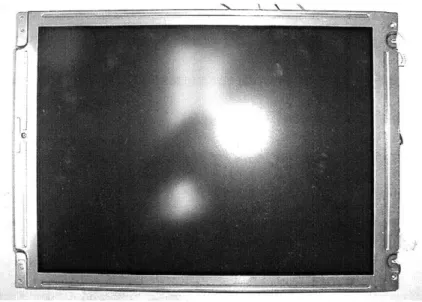
Figure 4.4: The working system. The photographer is displayed...61
Figure 4.6: Control signal propagation through the DCT chipset. ... 63
Figure A. 1: Video datapath, Bt829A video decoder...70
Figure A.2: Video datapath, first frame buffer. ... 71
Figure A.3: Video datapath, DCT and IDCT processors...72
Figure A.4: Video datapath, second frame buffer and LCD inerface...73
Figure A.5: DCT programming ROM, switch/LED interface, and clock generation...74
List of Tables
Table 2.1: Bt829A pin descriptions ... 23
Table 2.2: IDT7008 pin descriptions for each of two ports... 29
Table 2.3: DCT coder pin descriptions... 31
Table 2.4: IDCT decoder pin descriptions... 33
Table 2.5: Sharp LCD pin descriptions (signal polarities for 640x480 mode)... 35
Table 3.1: FSMs that control the video datapath... 45
Chapter 1
Introduction
1.1 Motivation for Low-Power Video Processing
Throughout the 1990s, multimedia and wireless communication have been two major
driving forces behind technology. As computing power and storage have kept pace with
Moore's Law, multimedia computers supporting high-quality digital video and sound have
become a reality. In response to the increasing popular demand for "anytime, anywhere"
communication, great advances have been made in wireless telephony and networking.
With these technologies firmly in place, the next step appears to be a combination of
wireless and multimedia technology. Potential applications could include the replacement
of the cellular telephone with a wireless video communicator, perhaps a product closely
resembling Dick Tracy's fanciful "two-way wrist communicator" which, until recently,
has been limited to the realm of science fiction.
The technology necessary for such a device is already in place. PCS cellular networks
currently implement digital communication on support small, lightweight handsets.
Mobile laptop computers can play movies and support videoconferences. However, the
biggest challenge, power consumption, is yet to be conquered. For battery-powered
devices, energy consumption can be as significant an issue as performance. Any cellular
telephone or laptop computer user will attest to this.
How difficult is the task of engineering a low-power "wireless multimedia
communi-cator"? Suppose that we were to implement such a communicator with a 1.8-volt, 233
MHz Pentium MMX processor, a common processor for laptop computers in early 1999.
"AA" battery, much like a pager. A high-capacity NiMH "AA" cell has a capacity of 1.25V * 1.45 AH * 3600 sec/H = 6500 Joules [1]. The processor, when fully utilized, dis-sipates 5.3 Watts of power [2][3], and would run for about 20 minutes before requiring a
new battery. This estimate does not account for the power consumption of the display, as
well as the wireless transceiver, which is typically the largest power consumer in wireless
devices, would further reduce battery life.
Even if we were to replace the Pentium processor with a processor specially designed
for low power consumption, such as a StrongARM microprocessor, we would still not be
able to achieve days or weeks of continuous operation from a small, lightweight source of
power. Any general-purpose processor, even one designed for low power consumption, is
not sufficient. The ideal solution is a custom processor designed from scratch and
opti-mized specifically for low-power manipulation of video data. In general, whenever low
power consumption is a primary design goal, every component must be custom-designed
to minimize the energy used. After all, a system consumes as much power as all of its
indi-vidual components. A single, inefficient component will dominate the power consumption
of the whole system.
1.2 The Wireless Camera Project
The ultra-low power wireless camera project is a demonstration of recent advances in
low-power circuitry applied to a complete wireless video system [4]. The project is being
undertaken by the Microsystems Technology Laboratory (MTL) in the Department of
Electrical Engineering and Computer Science.
The low-power wireless camera collects video data and transmits the data to a base station for further processing and display. The system can be conceptualized by the block diagram in Figure 1.1. The transmitting section consists of the sensor, an analog-to-digital (A/D) converter, a compression and coding section, and a transmitter. The image sensor
captures an image in analog form. The A/D digitizes the analog image. Next, compression
logic reduces the data rate to satisfy the transmitter's requirements, and coding logic
encodes the data with an error correction scheme. Finally, the transmitter sends this binary
stream to a base station (a personal computer with additional hardware on an expansion
card), where the image data is decoded, decompressed, and displayed. Students and
fac-ulty within MTL are optimizing each "block" of the wireless camera for minimal power
consumption.
Compression Radio
Imager A/D DCT & Tx
Coding
Low-Power Wireless Camera
Radio Decomp.
Base Station Rx & IDCT Display Decode
Figure 1.1: Block diagrams for the wireless camera project.
1.3 The Discrete-Cosine Transform and the DCT Chipset
Among the first devices to emerge from the wireless camera project are an
ultra-low-power discrete-cosine transform chipset. One device performs a forward discrete-cosine
transform; another performs the inverse operation. These devices can fill the DCT and
IDCT blocks in Figure 1.1. This chipset was designed by Thucydides Xanthopoulos. The discrete-cosine transform operation performed by this chipset is one of many
fre-quency-domain transforms and resembles the well-known Fourier transform in this
complex eCJt. In video applications, the data is two-dimensional, and a two-dimensional DCT is required. The forward DCT for an 8x8 block of pixels is defined as
X[u,v] X[' ] = c[u]c[v] 4 1 x[, j]cos((2i+ 1)u ~, cos(22j v (1.1)
iCs 16 J 16
i=0j= 0
with c[u] = 2-1/2 for u = 0 and c[u] = 1 for all other u.
The corresponding inverse is defined as
7 7
x[i, j] = I c[u]c[v]x[u v]cos((2i+ 1)uxCOS((2j+ 1 )vn) (1.2)
u = 0v = 0
with c[u] defined in the same way as the forward DCT.
The DCT facilitates the compression of image data. When applied to a two-dimen-sional block of pixels, the transform removes spatial redundancy by resolving the image data into an orthogonal basis of cosines. The resulting block of decorrelated spatial coeffi-cients is easier to quantize and compress, as seen in Figure 1.2. This property of the DCT is the motivation for its use in the MPEG video compression standard [5][6], as well as the data compression and decompression paths for the wireless camera project.
2-D Block of Pixels 2-D Array of DCT Coefficients
Figure 1.2: Block of pixels and its discrete-cosine transform.
This DCT chipset uses two general techniques to minimize power consumption [3]. The first is a set of novel data-dependent, power-aware algorithms. For instance, the
algo-rithm performs varying amounts of computation for each pixel instead of "butterfly"
mul-tiplications on all the data. The processor analyzes the input data and dynamically reduces
the precision of computations on low-magnitude or highly correlated pixels to conserve
power. Furthermore, when power is limited, the processor limits the precision of the
com-putation so that image quality degrades gracefully as available power is reduced.
The second technique for minimizing power dissipation is voltage scaling. The chipset
is designed to run on the lowest voltage possible for the amount of computation required.
Since the energy consumed by a device is proportional to the square of the input voltage,
designing the chip to operate with lower voltage can provide a significant reduction in the
energy consumed.
The DCT processor consumes an average of 4.38 mW at 1.56V when run at 14 MHz,
and the IDCT consumes 4.65 mW at 1.32V and 14 MHz. A 233 MHz, 1.8 Volt Pentium
MMX processor running a DCT algorithm in software would consume at least two orders
of magnitude more power than this low-power processor.
1.4 A Demonstration System
This work is the first system-level proof-of-concept of the wireless camera project's core
datapath. Up to the present, the focus the project had been the design of the individual
low-power components. With the focus now moving toward system-level integration, a
complete demonstration is necessary.
This system is also the first real-world evaluation and demonstration of the low-power
DCT and IDCT processors, the first complete products of the wireless camera project. Before this demonstration system was complete, the functionality and power consumption
levels of these processors had been evaluated through software simulations and with test
vectors downloaded to the chips from a PC. These tests used still-image data and were
This system demonstrates the transform, quantization, inverse transform, and display of
image data all at once, and in real-time. Furthermore, this system displays full-motion
video limited only by the images on a videotape, camera lens, or television broadcast, so
that the performance of the chipset can be evaluated in truly "real-world" situations.
Above all, this work is a challenge in real-time system design. Real-time data
process-ing requirements of this system adds a substantial degree of complexity to a design. The
successful design and implementation of this demonstration system requires careful
design and engineering methodologies to promote simplicity and robustness.
1.5 Implementation Overview
This demonstration system is intended to model the video processing datapath of the
wire-less camera as closely as possible. The focus of the demonstration is the DCT chipset, the
most recently completed components of the wireless camera project. The remaining
blocks in the diagram are replaced one-for-one with off-the-shelf devices. For this
demon-stration, a versatile and compelling demonstration of the completed low-power stages is
more important than the optimization of the entire system for power consumption. Rather
than focusing on the individual components, as others within MTL already are, this work
focuses on system integration.
NTSC NTSC
Input Decoder DCT IDCT Display
Device
Figure 1.3: Adaptation of LPE for this work.
The block diagram for the wireless camera can be adapted for this demonstration sys-tem per Figure 1.3. In place of the sensor/camera, this syssys-tem is designed for an arbitrary
to serve as the image source. Any device capable of generating an NTSC signal-most
every TV, VCR, and video camera used in the United States-can provide a video input to
this demonstration. In place of the A/D converter is an off-the-shelf NTSC video decoder.
Video decoders are readily available and are common in devices such as multimedia cards
for personal computers. Compression requires two steps: a frequency-domain transform
followed by frequency-domain quantization and compression logic. Both are available on
the low-power DCT chip, so there is no need to add an off-the-shelf solution.
Radio transmission and reception are not implemented in this demonstration. This
sys-tem simply passes the compressed output of the DCT coder directly to the IDCT device.
This not only eliminates a tangential source of complexity but also allows the entire
sys-tem to be implemented on a single, portable printed circuit board.
Without a radio communication link, there is no need for a complete base station to
receive and process transmitted data. A video display is sufficient, and a commercial
flat-panel LCD display suits this purpose. As the display provides digital video inputs, it can
be driven directly by the system without any additional D/A conversion.
1.6 Design Requirements and Goals
Specifications for data rate and format are taken directly from the specifications for
wireless camera project. This system processes thirty non-interlaced frames of video per
second. Each frame consists of either 128x128 pixels or 256x256 pixels, with eight bits of
grayscale per pixel. Only the higher resolution is supported in this demonstration.
Because this system is a testbed for the LPE datapath and the DCT/IDCT chipset, the
usual goals of test and demonstration systems apply. Flexibility and versatility are
essen-tial; the system should be able to simulate different operating scenarios with a minimum
of effort and intervention. Portability is also a worthwhile goal. For portable
con-nection to a computer. Since a testing environment can place strenuous demands on the
components under evaluation, the design should be able to isolate and expose bugs and
problems. After all, debugging is a primary use of test systems.
As the demonstration system is not intended for large-scale production, common
com-mercial issues such as cost, the large-scale availability of components, and user interface
are secondary. The primary goal is a successful, working design that offers a compelling
Chapter 2
The Video Data Path
This chapter introduces the components that form the main video datapath of the
demon-stration system. Beginning with a conceptual block diagram, off-the-shelf devices are
combined with the DCT chipset to realize each of the blocks. These devices are
docu-mented in this chapter. The clocking requirements for the datapath are also considered.
Reflecting on the chosen design, it becomes clear that modularity and abstraction are
essential for a successful, robust datapath.
2.1 High-Level Block Diagram
NTSC NTSC Frame Frame
Input Decoder Buffer DCT IDCT Buffer Display
Device
Figure 2.1: Block diagram of the real-time video datapath.
The full video data path consists of seven stages. An NTSC source generates an analog
video signal. A video digitizer converts the analog signal into a series of digital still
images, or frames. A ping-pong frame buffer stores and formats each frame for further
processing. The DCT coder transforms each frame into the frequency domain and
option-ally performs rudimentary quantization. The IDCT decoder then decodes the coefficients
and generates pixels. A second frame buffer re-assembles the frames, and a video display
Each of the "blocks" of the above diagram are implemented with one or two devices.
The NTSC decoder is realized by a Brooktree Bt829A video decoder, a single-chip device
that digitizes an NTSC video signal and provides a convenient digital output. Each frame
buffer is implemented by a pair of IDT7008 static RAM devices. The entire frame buffer
is capable of storing up to two full frames, one frame per IDT7008. The DCT and IDCT
stages are the ultra-low-power processors to be tested. The video display is a Sharp
active-matrix LCD. Figure 2.2 shows the new block diagram with the "blocks" replaced by the
selected components.
NTSC Bt829A SRAM Low- Low- SRAM Sharp
Input Video Frame Power Power Frame LCD
Device Decoder Buffer DCT IDCT Buffer Display
Figure 2.2: Block diagram with the chosen components.
2.2 The NTSC Decoder
The NTSC decoder receives an analog NTSC video signal and produces a digitized
eight-bit grayscale image that can be passed through the video datapath. As NTSC is an ubiqui-tous standard for analog video in the United States, an NTSC interface allows for versatile
demonstrations with a variety of video input devices.
The NTSC analog signal is digitized with the Bt829A video decoder. The Bt829A is a single-chip video digitizer produced by Rockwell Semiconductor [7]. The device supports NTSC, PAL, and SECAM formats as input and provides a digital YCrCb output with eight bits of luminance (brightness) and eight bits of chrominance (color) data. Image
parame-Figure 2.3: The Bt829A video decoder.
ters such as scaling, frame rate, and contrast can be adjusted by programming the device
on startup. Table 2.1 describes the pins most relevant to this work.
Pin Mode Function
YIN analog analog composite input for NTSC
SCL, SDA I/O Clock and data lines for 12C serial bus for device
pro-wired gramming.
AND
I2CCS I LSB of 8-bit 12C device address for this chip. RST I Resets device to default state.
XTOI I NTSC clock oscillator signal (28.636 MHz). VD[15..8] 0 Digitized luminance output in 16-bit mode. VD[7..O] 0 Digitized chrominance output in 16-bit mode.
DVALID 0 Data Valid. High when a valid data (image pixel or blank-ing) data is being output. Low during blanking intervals or when no pixel is output due to scaling.
ACTIVE 0 Active Video. High when an the active image area (as opposed to a blanking interval) is being digitized. VACTIVE 0 Vertical blanking. Low during active vertical lines. FIELD 0 Odd/even field indicator. By default, "1" denotes that an
odd field is being digitized.
HRESET 0 Horizontal Reset. Falling edge denotes new horizontal scan line.
Pin Mode Function
VRESET 0 Vertical Reset. Falling edge denotes a new field. QCLK 0 "Qualified Clock." Gated such that edges occur only
when valid, active image pixels are being output.
CLKx1 0 14.31818 MHz clock output. All output signals are timed with respect to this clock.
OE I Tri-state control for certain outputs. Effect of the pin can be programmed through register OFORM.
Table 2.1: Bt829A pin descriptions
To decode an NTSC video signal, the Bt829A requires only two active inputs: a
com-posite analog NTSC signal at pin YIN, and a 28.636 MHz clock at XTOI. Using the clock
as a reference, the Bt829A samples the analog signal at YIN, recovers line, field, and
frame boundaries, and distinguishes between valid image data and supplementary data
(such as closed-caption information) included in the blanking intervals between each line
and field. Digitized pixels from each field are output on the 16-bit output VD. The eight
most significant bits represent luminance information. The eight least significant bits
rep-resent chrominance and can be ignored by this demonstration system.
The VD output is clocked at 14.318 MHz, half the input clock frequency. The Bt829A
provides a 14.318 MHz clock output on CLKx1 for synchronization with this output. Due to blanking intervals, decimation, and other processes that reduce data throughput, a valid
pixel is not output at every clock. Hence, the Bt829A provides a variety of status signals, including DVALID, ACTIVE, VACTIVE, and FIELD, to indicate what portion of the NTSC video stream is currently being digitized. These signals are described fully in table 2.1. Figure 2.4 illustrates the output interface discussed here; the white VD blocks indicate valid data
When the system is powered on, the Bt829A must be reset by asserting the RST line
VD15:01 / DVAUD ACTIVE CLKx1 or CLKx2 QCLK
Figure 2.4: Output timing for the Bt829A, reproduced from [7].
parameters for digitization, such as the output frame rate, size of the digitized image,
brightness and contrast, and impulse response lengths for the decimation filters. These
parameters are loaded into the device through the SCK and SDA lines, which operate
under the serial 12C (Inter-Integrated Circuit) bus protocol [8].
For this system, the Bt829A was initially programmed to produce a 256x256 image
with no temporal decimation and no image quality adjustments. The Bt829A would be
programmed to digitize both fields of every frame to form a 640x480 image at 30 frames
per second. The image would then be downsampled to 256x256 through decimation filters
in both dimensions. Unfortunately, using both the even and odd fields in this way caused
jagged horizontal lines with animated images.
An alternative approach, dropping the entire odd field in each frame, produced better
results. Dropping one field halves the number of vertical lines from the NTSC standard of
480 to 240, resulting in sixteen fewer lines than the 256 lines required by wireless camera.
It was decided that the better quality of the field-dropped 256x240 image was preferable to
2.3 The "Ping-Pong" Frame Buffer
Frame buffers provide flow control and data reordering between the video and coding
stages in the system. The video stages (the NTSC decoder and LCD screen) require
raster-ordered data: pixels are generated or received in left-to-right, top-to-bottom order.
Further-more, these devices are bursty; an NTSC signal, for instance, contains retrace periods
where no image data is being sent. As we will discuss below, the DCT and IDCT
proces-sors require a completely different pixel format, and they are best suited for processing
data at a constant throughput. Buffering pixels between such stages provides the system
with the space and time to perform these format conversions.
2.3.1 Design of a Dual-Port Frame Buffer
A buffer receives data from one stage of the system, stores it, and sends the data to the following stage. Since the buffer is being read and written to simultaneously, it must
func-tion as a dual-port device. Since data must be reordered and moved at potentially different
rates, the two ports should be as independent as possible.
The most robust design is a frame buffer that is large enough to store two full 256x256
frames, or 2*28*28 = 217 bytes = 128 kilobytes. With two full frames of storage, the stage
that writes the buffer is guaranteed enough storage for a full frame of data, while the stage
that reads the buffer is guaranteed a full frame of valid data. The buffer is partitioned into
two halves of one frame each, and the reading and writing stages read alternate halves of
the buffer and swap in a ping-pong fashion at every frame. While more complicated
schemes can perform a similar function with less memory, they reduce the timing
flexibil-ity of the reading and writing stages.
This type of ping-pong buffer is readily implemented with off-the-shelf memory
devices. Two prominent issues arise in such a design. The first is the choice of static versus
mem-ory with additional control circuitry to simulate a second port. This design chooses
dual-port static RAMs, but we first discuss the alternatives and the reasons for their dismissal.
One possible implementation for the frame buffers is a dynamic RAM (DRAM)
instead of a static RAM. As DRAM is available in larger sizes than SRAM, a
DRAM-based frame buffer can easily be implemented by a single chip. DRAM is also less
expen-sive than SRAM. Unfortunately, DRAM requires additional refresh and addressing
cir-cuitry that would increase the complexity of the control logic. Additional logic requires
additional macrocells on a programmable logic device. The task of refreshing the DRAM
also adds more constraints on the timing requirements of incoming and outgoing data
because data can not be read or written while the memory is being refreshed. In a
commer-cial, high-volume product, the lower cost of DRAM would justify the additional control
circuitry required. For a prototype system such as this one, where logic complexity is a
greater enemy than cost, static RAM is the better choice.
Another design issue is single-port versus dual-port SRAM. If a single-port SRAM is
clocked at twice the frequency of the incoming or outgoing data, the memory can be read
and written on alternate cycles. The cost in additional control complexity is seemingly
small, and like DRAMs, single-port SRAMs are available in larger sizes and lower cost
than their dual-port cousins. However, two design issues make dual-port SRAM the more
favorable option.
First, the use of a single-port SRAM would require tri-state outputs on the device
driv-ing the SRAM, as well as an additional eight-bit register to latch the outgodriv-ing data from
the SRAM for the reading device. This circuit is illustrated in Figure 2.5. The IDCT
device, which writes the second frame buffer in this system, was not equipped with
tri-state outputs. Hence, a frame buffer based on single-port SRAM would require an
single-SRAM
DATA_- OUTH- D 0 --- DATA_ IN
Tri-State
SRAM Driver Reg. SRAM
Writer Reader
Figure 2.5: Alternative buffer design with a single-port SRAM.
chip implementation of NTSC decoding, this heterogeneous three-chip solution seems
sig-nificantly less elegant.
Second, the clock rates of the two devices writing to and reading from the frame buffer
are likely to be different. A true dual-port static memory can support fully asynchronous
access to both ports. A scheme that simulates two ports through control logic would require additional synchronization logic.
After considering the drawbacks of single-port memories or DRAM, dual-port static
RAM was deemed the best choice for implementing a frame buffer. The IDT7008 memory
is chosen for this design.
2.3.2 Application of the IDT7008 Static Ram
The IDT7008 was the largest single-chip, 8-bit wide, dual-port static RAM that could be located at the time of this work [9]. The IDT7008 is a 216 byte memory, enough for a single frame of 256x256, eight-bit video. Each frame buffer is implemented as two IDT7008 devices operating in parallel to simulate 217 bytes of dual-port RAM.
The IDT7008 is an asynchronous device. Each port is equipped with a R/W line to select whether the port is reading and writing data, an OE line for tri-stating the port, and
Figure 2.6: A pair of IDT7008 static RAM devices.
two chip enables, CEO and CEI, that are internally ANDed together into a single enable
signal. The two chip enable lines allow several IDT7008 devices to act as a single, deeper
SRAM. Semaphore signalling between ports and arbitration logic are also provided, but
they are not necessary for this design.
Pin Mode Function
A[15..0] I 16-bit address
R/W I High to read SRAM, low to write SRAM CEO, CE, I Chip selects. CE = (CEO AND CEI) OE I Output enable. High to tri-state the port.
1I/O[7..0] 1/0 8-bit port. For SRAM reads, data appears here. For SRAM writes, data should be driven here.
Table 2.2: IDT7008 pin descriptions for each of two ports.
Figures 2.7 and 2.8 illustrate the reading and writing interfaces for each port. A port is
read by driving both CE lines active, driving R/W high, and presenting a valid address on
the address lines. After the last of these conditions has been fulfilled, valid data appears on the port after a brief delay. The memory is written by driving both CE lines active and
driving R/W low. After a brief delay, the data at the port is written into the desired address
always a good idea to drive OE high any time a write is about to occur. For write
opera-tions, it is essential that the controller set-up and hold a valid address on the SRAM around
a write cycle so that spurious writes to unintended portions of the memory do not occur.
ADDR
OE
R/W
DATAouT
Figure 2.7: Read interface for the IDT7008, reproduced from [9].
Figure 2.8: Write interface for the IDT7008, reproduced from [9].
With the buffer realized by two distinct SRAM devices, a natural implementation of the ping-pong scheme is for one SRAM to receive data from the previous stage while the other SRAM sends data to the next stage. Each memory stores a full frame of data. When
both reading and writing transactions have completed, the two devices switch roles. The presence of two chip select lines on each port greatly assists this procedure; the additional
chip selects on each port can act as the high address bit and select which SRAM is active
for each stage.
In retrospect, the timing requirements for reading and writing an asynchronous SRAM
could have been avoided with a synchronous SRAM. The IDT70908, a 216 byte dual-port
synchronous memory, provides a clocked control interface than the IDT7008.
2.4 The DCT Processor
The low-power DCT processor receives two-dimensional blocks of pixels and outputs the
corresponding block of DCT spectral coefficients. Table 2.3 describes the functions of the
DCT's pins.
Figure 2.9: The DCT processor (left) and IDCT processor (right).
Pin Mode Function
DIN[7..O] I 8-bit pixel input
DOUT[11..0] 0 12-bit DCT spectral coefficient output
LPEout 0 Serial output for selected DCT coefficients. Output repre-sents 8:1 compression of initial pixel data.
SBIN I Start Block In. Denotes that the input pixel is the first pixel in a block of 64.
SBOUT 0 Start Block Out. Denotes that the output DCT coefficient is the first in a series of 64.
Pin Mode Function
RESET I Resets device to default, unprogrammed state. TDI, TMS, I JTAG-compliant testing and programming pins. TCK, TRST
Table 2.3: DCT coder pin descriptions.
The DCT processor receives blocks of 64 eight-bit pixels, one pixel per clock cycle.
The SBIN input must be pulsed high during the first pixel in each block to signify the start
of a new block. No pause is necessary between blocks; the first pixel of a new block may
immediately follow the last pixel of the previous block. Incoming pixel values are latched
on the falling edge of the clock.
After a latency of 97 cycles from the first pixel, sixty-four DCT spectral coefficients
begin to appear at the output. Coefficients are output in two ways, as a 12-bit wide output
as well as a serial compressed output. The 12-bit output operates analogously to the pixel
input. Like the input pixels, which are input over 64 consecutive clock cycles, DCT
coeffi-cients are output over 64 consecutive clock cycles. Like SBIN, the SBOUT signal is
pulsed high during the first coefficient to signify the start of a new group of coefficients.
A serial output is produced on the LPE pin. The purpose of this pin is to provide a rudimentary form of 8:1 data compression. This output provides eight DCT coefficients
per pixel block, at a precision of eight bits per coefficient. Only coefficients 0, 1, 2, 8, 9, 10, 16 and 17 are output. Hence, over 64 clock cycles, the LPE pin delivers eight coeffi-cients of eight bits each, for a total of 64 bits-a reduction of 8:1 from the 64 bytes of
input pixels.
On power-up, the DCT must be reset by asserting its RESET line high for several
clock cycles. Six registers on-board the DCT must also be programmed through a JTAG-compliant interface. These registers determine parameters for the transform computation.
2.5
The Inverse Discrete-Cosine Transform Processor
Since the DCT and IDCT processors were designed by the same student, it is not
surpris-ing that they have nearly identical interfaces. Table 2.4 summarizes the functions of the
relevant pins. Coefficients are received by the IDCT processor in groups of 64. The
coeffi-cient input is 12 bits wide; there is no serial input analogous to the DCT's serial output.
The SBIN signal must be pulsed high during the first coefficient. After a latency of 90
cycles from the first coefficient, a block of 64 pixels is produced on an 8-bit output. The
SBOUT signal is pulsed high on the first pixel of each block. The SBIN and DIN lines of the IDCT are directly compatible with the corresponding outputs of the DCT. These two
devices may simply be connected together.
The IDCT processor must be reset by holding its RESET line high. No device
pro-gramming is required.
Pin Mode Function
DIN[1 1..0] I 12-bit DCT coefficient input DOUT[9..0] 0 10-bit pixel output
SBIN I Start Block In. Denotes that the input coefficient is the first in a series of 64.
SBOUT 0 Start Block Out. Denotes that the output pixel is the first in a block of 64.
RESET I Resets device to default, unprogrammed state. Table 2.4: IDCT decoder pin descriptions
2.6 The Video Display
The Sharp LQ14D412 is an active-matrix TFT liquid crystal display that supports
640x480 pixels in 24-bit color. Unlike conventional computer monitors which require a
partly analog interface, the synchronization, clock, and data signals for the Sharp LCD are
signals and drives the actual display. This level of separation between the display's
inter-face and its actual pixels results in a remarkably flexible interinter-face. For instance, the
num-ber of pixels in a line or lines in a frame may vary without introducing jitter in the display,
and arbitrarily low refresh rates will not cause flicker. The latter property is excellent for a
30 frame per second video system, as computer monitors are driven well above 60 Hertz for flicker-free images.
Figure 2.10: The Sharp LCD.
As summarized by table 2.5, the control interface is similar to standard VGA. Edges
on HSYNC and VSYNC delineate the start of a new line or frame of video. For its
640x480 display mode, in which every pixel on the LCD is being utilized, the LCD
requires roughly 800x550 clock cycles, maintaining a sort of backward compatibility with
analog displays which required a retrace interval between each line and frame. The data
Pin Mode Function
HSYNC I falling edge indicates start of horizontal scan line VSYNC I falling edge indicates start of new 640x480 frame ENAB I rising edge indicates start of valid pixel data in a line RED[7:0] I eight-bit RGB pixel values
GREEN[7:0] BLUE[7:0]
Table 2.5: Sharp LCD pin descriptions (signal polarities for 640x480 mode).
Since the frames passing through the system are 256x240 grayscale, this
demonstra-tion system does not require the full display area of this LCD. Addidemonstra-tional control logic is
responsible for displaying a 256x240 grayscale image attractively on the LCD display.
The choice of the Sharp LCD was not without consideration. In its favor are a simple,
abstract digital interface with no minimum refresh rate, a crisp, clear image, and
immedi-ate availability at the time of design. However, there are two significant
disadvantages-this particular LCD screen is both large and somewhat non-standard. Its large size makes
portable demonstrations more cumbersome. The 640x480 pixel display is unnecessarily
large for display of a 256x240 pixel image; pixel doubling would only make the image
more grainy and detract from the demonstration. A non-standard interface port presents
two additional problems. First, it requires a custom adapter, which was fabricated as a
PCB for this work. Second, it precludes the use of other output devices, such as a
com-puter or television monitor, in contrast to the versatile NTSC video input.
There are several alternative display options. An NTSC encoder chip, analogous to the
Bt829A decoder, could drive any standard NTSC video display. Although the versatility of
this solution is appealing, the quality of NTSC displays, however, is generally lower than
high-quality, non-interlaced displays, but adding a VGA driver interface would require at
least one additional block to the system-we are basically adding a video card to the
sys-tem!
2.7 Clocking Requirements
As suggested by Figure 2.11, the system can be divided into three distinctly different
clocking regimes, one each for the Bt829A, the DCT/IDCT chipset, and the LCD display.
NTSC Bt829A SRAM DCT IDCT SRAM Sharp
Input Video Fra e Coder Decoder Frame LCD
Device Decoder Buffer Buffer Display
analog 14.318 MHz| 3 MHz 12 MHz
Figure 2.11: Timing requirements for the real-time video datapath.
The Bt829A requires a 28.636 MHz clock to decode an NTSC video signal. Pixel data are output at half this frequency, 14.318 MHz. These clocking requirements are fixed by the Bt829A.
The LCD offers more clocking flexibility than the Bt829A. Documentation for the LCD suggests a 25 MHz clock for a 60 frames/second rate, assuming about 750x520 clock cycles per frame. (Recall that the number of clocks per frame is higher than the number of pixels on the screen to simulate some horizontal and vertical blanking time.) Because this system is running at 30 frames/second, a clock rate close to 12.5 MHz would be ideal. A rate of 12 MHz was chosen both for the ready availability of clock oscillators and the ease of numeric computation.
The DCT and IDCT support a wide range of clock frequencies; they can operate at tens of megahertz, or tens of kilohertz. Their clock should be chosen fast enough so that
the incoming pixel data can be processed in real-time without frame drops. Since the
frame rate is 30 frames per second at 256x256 = 216 pixels per frame, the chipset must
process 1,966,080 pixels per second. This is the minimum allowable clock rate for the
chipset. While a 2 MHz clock is sufficient, it would leave little idle time between frames,
imposing strict timing requirements on the surrounding stages. A more reasonable choice
is a 3 MHz clock, which provides a generous 50% margin of safety. Another compelling
reason for choosing a 3 MHz clock is that it is exactly one-fourth of 12 MHz, the clock
rate chosen for the LCD. The DCT chipset can now operate synchronously with the LCD
section and the intervening frame buffer.
2.8 A Design Lesson: Modularity and Abstraction
A modular design divides its functionality among a number of distinct units, or "mod-ules," allowing each module to be designed and tested independently. Modular design is
evidenced by block diagrams, in which designers categorize functionality into distinct,
independent blocks. In a well-designed modular system, each module presents its
func-tionality through a simple input-output interface, and hides the low-level details of its
operation in a metaphorical "black box" [10]. Functionality is abstracted into modular
units.
As each block of this system is implemented by a single device (or pair of devices), the
actual hardware maintains the level of abstraction offered by a block diagram. The video
input and output, in particular, provide a tremendous amount of functionality through a
simple digital interface.
The Bt829A, for instance, carries out all NTSC decoding and digitizing on a single
device. Using the single-chip Bt829A eliminates the need to work with the lower-level
ele-ments that are required for video digitization, such as A/D converters, phase-locked loops,
hidden from the system; the five discrete analog components connected to the Bt829A
occupy little more than a square inch on the circuit board. Since the goal of this project is
to design a real-time video processing system, and not to design a better NTSC decoder,
the Bt829A provides a valuable abstraction of digital video input.
The Sharp LCD screen provides a similar abstraction for video output. Its versatile,
all-digital interface conceals the details of drawing and refreshing the display.
Further-more, as discussed in section 2.6, the LCD's built-in controller can withstand variations in
line length, number of vertical lines, and refresh rate. The LCD can be treated as a black
box for digital video output.
The clocking discussion of section 2.7 suggests that an even higher-level abstraction is
present in this design. There is a fundamental reason for the three different clocking
regimes: different sections of the system process data in different ways. The video input
and output stages require relatively high clock rates, since each of these stages process
480-line frames with long retrace intervals between frames. The DCT and IDCT
proces-sors process a smaller, 256x256 frame, and can operate on a slower clock. Furthermore, these stages require different pixel formats. The video input and output stages work with pixels in a raster-scan (left to right, top to bottom) order, while the DCT chipset works with pixels in two-dimensional, 8x8 blocks.
It is evident that there are three high-level video functions in this system: digitization, processing, and display. Furthermore, much of the complexity in this system arises from the interconnection of these three elements. The solution employed in this system, the dual-port frame buffer, isolates each of the three high-level functions. These buffers intro-duce the necessary latency and memory to reorder pixels and alter their rate of flow, and to allow each of these three major sections to operate asynchronously. In other words, the frame buffers are physical abstraction barriers between each of the three high-level func-tions in this system.
Chapter 3
The Control Subsystem
This chapter discusses the control logic for the demonstration system. Control logic is
implemented on Cypress programmable logic devices using VHDL. The devices realize a
series of small finite-state machines that control small segments of the system. The FSMs
control the interfaces of the video data path and device initialization. The wise use of
pro-grammable logic yields a design that is resilient to growth and change.
3.1 The Cypress CPLD
Control logic is stored in complex programmable logic devices (CPLDs). The particular
device chosen for this work is the Ultra37256, manufactured by Cypress Semiconductor
Corporation [11]. Ultra37256 devices consist of 256 macrocells arranged into 16 logic
blocks. The devices are "in-system reprogrammable," meaning that they can be
repro-grammed even after placement onto the circuit board. Logic is prorepro-grammed in VHDL, a high-level logic description language, and is compiled and simulated in Warp, a propri-etary integrated development environment for Cypress programmable logic devices.
The CPLD chosen for this work is a CY37256P154AC. The 160 denotes its
160-pin package, and the 154 denotes its stated maximum operating frequency of 154 MHz.
Out of its 160 pins, 128 pins are available for use as input or output signals. 128
cells are associated with these 128 pins, one pin per macrocell. The remaining 128
macro-cells are "buried," for their values are not accessible from a pin. These macromacro-cells can be
used to hold state, intermediate logic, or other logic values that need not appear at the
out-puts.
Prior successes of other groups in MTL with this device family [12][13] greatly
influ-enced its selection. The 154 MHz version of the Ultra37256 was the fastest available when
the system was designed. Despite its higher cost over slower models, it was chosen to
min-imize propagation delay through the control logic.
As such a high-speed CPLD may seem excessive for a system whose fastest oscillator
is 28.6 MHz, a detailed discussion of CPLD speed ratings is worthwhile. The maximum
operating frequencies for CPLDs can be somewhat misleading; the actual maximum clock
speed for a CPLD in a world system is dependent on the complexity of the logic
real-ized within the system. The CY37256P160-154AC, though rated for 154 MHz, has a
max-imum propagation delay of tpD = 7.5 ns and a setup time of tS = 4.5 ns. Hence, for a simple
circuit that requires a CPLD output to be fed back into an input, we should operate the
device at no higher than 1/(7.5 ns + 4.5 ns) = 77 MHz, half the rated maximum frequency.
Perhaps the 154 MHz rating indicates that computation can be performed on both phases
of a 77 MHz clock with careful pipelining of the logic within the device.
Second, signals that pass through the CPLD's interconnect matrix n times incur n
times the propagation delay tPD. Signals that arise from particularly complex VHDL
struc-tures, such as highly-nested IF statements and asynchronous overrides of clocked logic, tend to require more than one macrocell on the CPLD. Every time a signal moves from
one macrocell to another for further processing, it incurs an additional propagation delay.
Hence, propagation delays for some signals can be double or triple the rated
tPD-Third, even if the device could support computation at a 154-MHz clock frequency, it
would be unwise to use such a CPLD in a system with a clock frequency anywhere near
154 MHz. Doing so would imply that the other devices that interact with the CPLD have
zero delay! The actual maximum operating frequency depends on the sums of all the setup
times, hold times, and propagation delays in any path. Suppose that n devices in a critical
path with the CPLD, and for simplicity assume that all n devices have similar timing
requirements as the CPLD. For this path, the actual maximum operating frequency is the
CPLD's rated maximum operating frequency divided by n. With devices operating on
clocks as high as 28.6 MHz, choosing the fastest available Ultra37256 device no longer
seems like an extravagant decision.
3.2 Real-Time Control for the Video Datapath
Control logic is essential for managing the interface between devices in the video
datap-ath. When data is produced by one device, control logic ensures that the next device is
pre-pared to receive and process it.
3.2.1 Overview
Each stage, be it a frame buffer, coding chip, or display, operates in basically the same
way. A stage remains idle until signalled by the previous stage that a new frame is ready
for output. The stage then reads the video data and process it appropriately. When the
stage is ready to pass the frame's data on to the next stage, it produces a "frame ready"
sig-nal of its own, and begins sending data. Figure 3.2 depicts this conceptual view.
The first stage, the video decoder, produces the initial "frame ready" signal as it
New Frame Ready
Stage Next
Video Data Stage Video Data
Figure 3.2: Conceptual view of stage interactions.
depends upon the frame boundaries of the analog NTSC signal to control the flow of
frames through the entire system.
Note that the propagation of control signals is entirely one-way. When a stage sends
data, it need only signal the next stage that data will be on the way shortly. The sender
does not wait for any acknowledgment. The receiver is completely responsible for being
prepared for each new incoming frame. Assuming that this condition can be met, this
one-way flow of control and data greatly simplifies the interfaces between stages of the video
datapath.
Table 3.1 introduces the five FSMs that control the video datapath. Each is responsible
for controlling data flow at the interface between two adjacent devices in the datapath. The
NTSC, DCT, IDCT, and LCD state machines each manage the transfer of data to or from a frame buffer. The DCT and IDCT FSMs are further responsible for converting the
raster-order pixel data to and from the 8x8 pixel block format required by the DCT and IDCT
devices. The NTSC and IDCT FSMs, which operate the write (left) port of a dual-port
frame buffer, generate a "next frame ready" signal for the next FSM in the chain, for the
frame buffers, unlike the other stages in the datapath, are not capable of generating this
signal by themselves. The COMPRESS state machine binds the DCT output with the IDCT input. It is responsible for converting the DCT's serial output, when active, to a par-allel input for the IDCT.
FSM Duties
NTSC Manage data transfer between video decoder and first frame buffer Signal DCT state machine when a full frame has been loaded DCT Manage data transfer between first frame buffer and DCT coder
Reorder pixels in frame buffer into 8x8 block format COMPRESS Manage data transfer between DCT and IDCT devices
Perform serial-to-parallel conversion on DCT serial output IDCT Manage data transfer between IDCT and second frame buffer
Reorder pixels in frame buffer into raster format
Signal LCD state machine when a full frame has been loaded LCD Manage data transfer between second frame buffer and LCD
Generate LCD control signals
Table 3.1: FSMs that control the video datapath.
3.2.2 The NTSC State Machine
The NTSC state machine manages the flow of data between the Bt829A video decoder
and the write port of the frame buffer. This FSM toggles between one of two states. It is
waiting when idle, and loading when the Bt829A is digitizing an even field.
The waiting state is the FSM's idle state. The SRAM's port is disabled, and the address
counter is reset to zero. The FSM remains in the waiting state until the Bt829A signals the
arrival of an even field by driving both VRESET and ACTIVE to a logical zero. On the
clock edge following this condition, the FSM advances into the loading state and also
tog-gles WHICHRAM, the signal that selects which of the two SRAMs is being loaded by the
Bt829A. Toggling WHICHRAM also notifies the state machine that controls the DCT that
a new frame of data is available.
In the loading state, the FSM checks whether a valid pixel is being produced by the
Bt829A at every clock. If both DVALID and ACTIVE are high, the data byte that is output
port is enabled so that the pixel can be written, and the SRAM address counter is
incre-mented. If either DVALID or ACTIVE is low, the Bt829A data lines contain invalid data.
Hence, the port is disabled, and its address is held at its current value. Once 240 lines of
the image have been read, the FSM returns to the waiting state, where it remains until a
new even field is digitized.
(default transition) * waiting RAM addr <= OxOOO
RAM chip select <= disable
start of new even field?
(VRESET = ACTIVE =
'O'
end of field?and FIELD = 0) (RAM address = OxEFFF)
WHICHRAM <= WHICHRAM
if (DVALID = '1' and ACTIVE = '1') then:
loading RAM chip select <= enable
next RAM addr <= RAM addr + 0x0001
Figure 3.3: State transitions for the NTSC FSM.
3.2.3 The DCT State Machine
The DCT state machine manages the flow of data between the first frame buffer and
the DCT processor. Much like the NTSC state machine, it is implemented in two states,
waiting and loading. These states also serve analogous functions, except that data is read from the frame buffer and to the DCT coder.
Figure 3.3 illustrates the state transitions for the DCT FSM. The FSM remains idle in
the waiting state and polls the WHICHRAM signal from the NTSC state machine. Recall
that this signal is toggled by the NTSC FSM to signify that a complete frame has been

![Figure 2.4: Output timing for the Bt829A, reproduced from [7].](https://thumb-eu.123doks.com/thumbv2/123doknet/14675193.557790/25.918.127.752.140.346/figure-output-timing-bt-a-reproduced.webp)


![Figure 2.7: Read interface for the IDT7008, reproduced from [9].](https://thumb-eu.123doks.com/thumbv2/123doknet/14675193.557790/30.918.192.780.249.514/figure-read-interface-idt-reproduced.webp)