Advanced Nanofabrication of Thermal Emission Devices
byFergus Hurley
B.E. Electrical and Electronic Engineering University College Cork, Ireland 2006
Submitted to the Department of Electrical Engineering and Computer Science in partial fulfillment of the requirements for the degree of
Master of Science in Electrical Engineering
at theMASSACHUSETTS INSTITUTE OF TECHNOLOGY
May 2008bone, Q0081
© 2008 Massachusetts Institute of Technology. All rights reserved.
Signature of Author 9
' Fergus Hurley
Department of Electrical Engineering and Computer Science
' ' May 23, 2008
Certified by
S(
John G. KassakianProfessor of Electrical Engineering and Computer Science
-- Thesis Supervisor
Certified by .. . .. . .. . . ..
Ivan Celanovid Post Doctoral Researcher Thesis Co-Supervisor Accepted by
MASSACHUSETTS INSTITUTE
/
Terry P. OrlandoOF TEOHNOLOGY Professor of Electrical Engineering and Computer Science
Advanced Nanofabrication of Thermal Emission Devices
by
Fergus Hurley
Submitted to the Department of Electrical Engineering and Computer Science on May 23, 2008, in partial fulfillment of the
requirements for the degree of Master of Science
Abstract
Nanofabricated thermal emission devices can be used to modify and modulate blackbody thermal radia-tion. There are many areas in which altering thermal radiation is extremely useful, especially in static power conversion, lighting and sensor applications. Two specific thermal emission devices which show great promise include resonant thermal emitters and selective thermal emitters. It has been found from theory that resonant thermal emitters exhibit quasi-monochromatic and partially coherent thermal emis-sion when fabricated with a 2-dimenemis-sional photonic crystal structure in a high-dielectric low-absorption material such as silicon. This type of fabricated resonant thermal emitter has great potential for use as near-IR and IR sensors. Theory has also shown that selective thermal emitters fabricated in tungsten with a 2-dimensional photonic crystal structure can exhibit spectrally selective thermal emission. This type of fabricated selective thermal emitter can be used to increase the efficiency of thermophotovoltaic (TPV) systems by preventing the incident thermal radiation below the band-gap of the PV diode from reaching the PV diode.
This thesis explores the nanofabrication of a 2-dimensional photonic crystal silicon-on-sapphire (SOS) resonant thermal emitter which is now possible to fabricate due to advances in fabrication technology. Initially, the theory behind the SOS resonant thermal emitter which exhibits multiple resonant emission peaks is discussed. Next, an in-depth examination of the theory behind the technology used in the fabrica-tion the resonant thermal emitter is investigated. Then, the SOS resonant thermal emitter fabricafabrica-tion process and characterization which was performed is discussed. The results showed that it was possible to fabricate the required 2-dimensional pattern but that there were issues with the pattern transfer into sili-con, which needs to be further researched.
Thesis Supervisor: John G. Kassakian
Title: Professor of Electrical Engineering and Computer Science Thesis Co-Supervisor: Ivan (telanovi6
Acknowledgments
I would like to express my deepest gratitude to all the people with whom I have had the immense pleasure to study, teach and perform research with at MIT. In particular I wish to thank Professor John G. Kassakian, my supervisor for the opportunities he has provided me with and the support, encouragement and guidance he has offered me in my research and throughout my time at MIT. JGK truly is a legend.
I am very grateful to Dr. Ivan Celanovid, my co-supervisor for believing in me and providing me with the opportunity to work in the area of nanofabrication of thermal emission devices. His en-couragement and supervision has been a great asset and I have learnt an extraordinary amount from him about how to approach research problems. It has been a great privilege to work with such a fantastic researcher.
I would like to thank Natalija Jovanovic for helping me become established in the fab and for devoting time to supervising my day to day activities at the outset of my research. Her unique ability to instill motivation in me and assistance in digging deeper on the fabrication aspects of my research was invaluable.
My appreciation goes to all the staff and students in the Nanostructures Laboratory, the Technol-ogy Research Laboratory and the Exploratory Materials Laboratory at MIT. I am particularly grateful to Kurt Broderick, Jim Daley, Tim Savas and Donal Jamieson for all their help and guid-ance on the intricacies of fabrication. I would also like to thank all the administrators in the La-boratory for Electromagnetic and Electronic Systems and in the Department of Electrical Engi-neering and Computer Science for taking care of all the formalities.
I am grateful to all the students in the Laboratory for Electromagnetic and Electronic Systems for treating me with respect and helping me feel at home during my time in the lab. I would like to give a special thanks to all the inspirational characters that I have had the pleasure of becoming friends with through my involvement in EECS classes, the MIT Energy Cub and as residential advisor for the No.6 Club fraternity house.
Lastly, and most importantly, I wish to thank my family, whose love and support made this and everything else in my life possible and to whom I owe everything. You're the best!
Contents
1 Introduction ... 15
1.1 Thesis M otivation... 15
1.2 Thesis Outline ... 16
2 Therm al Em ission Devices ... 19
2.1 Photonic Crystals ... 19
2.2 Resonant Therm al Em itter ... 21
2.3 Selective Therm al Em itter... 22
3 Resonant Thermal Emitter Fabrication Technology... .. 25
3.1 Chem ical Vapor Deposition... 26
3.2 Spin Coating ... 29
3.3 Interference Lithography ... 37
3.3.1 Pattern Form ation... 40
3.3.2 Lloyd's M irror Interference Lithography ... 42
3.4 Anti-Reflection Coating ... 46
3.4.1 Index of Refraction ... 47
3.4.2 Thickness Calculation ... 49
3.5 Photoresists ... 50
3.5.1 Dose ... 51
3.6 Reactive Ion Etching ... 52
4 Resonant Therm al Em itter Fabrication ... 57
4.1 Deposition ... 58
4.1.1 PECVD Silicon Dioxide Hard-M ask ... 59
4.1.2 Spin Coating Anti-Reflection Coating ... 62
4.1.3 PECV D Silicon Dioxide Inter-Layer ... 66
4.1.4 Spin Coating Photoresist... 66
4.2 Lithography ... 68
4.2.1 Lloyd's M irror Interference Lithography ... 69
4.3 Etching ... 72
4.3.1 RIE Silicon D ioxide Inter-Layer... 73
4.3.2 RIE Anti-Reflection Coating ... 75
4.3.3 RIE Silicon D ioxide Hard-M ask... 77
Contents 5 Conclusion ... 81 5.1 Sum m ary ... 81 5.2 Future W ork ... 82 Appendix ... 85 Appendix A ... 85 References ... 89
-8-List ofFigures
Figure 2.1: Illustration of a 1-, 2- and 3-dimensional photonic crystal. Adapted from [5]... 19 Figure 2.2: 2-dimensional photonic crystal structure where a is the periodicity, d is the depth and 2r is the diam eter of the holes... 20 Figure 2.3: Simulated 2-dimensional silicon photonic crystal slab with 1 pmn periodicity and 400 nm diameter holes displaying anomalous emittance (non-blackbody) and thermal radiation intensity at 750 K and 1000 K. Adapted from [1] ... 21 Figure 2.4: Resonant thermal emitter 2-dimensional silicon-on-sapphire photonic crystal
structure ... 22 Figure 2.5: Simulated normal emittance of flat tungsten and a 2-dimensional tungsten photonic
crystal structure (1 pmn periodicity, 800 nm hole diameter and infinite hole depth). Adapted from [1]... 23
Figure 2.6: Selective thermal emitter 2-dimensional tungsten photonic crystal structure... 24 Figure 3.1: The three basic stages of the PECVD process: 1. chemical activation by electron impact, 2. transport of the activated species to the film surface and 3. bonding to the film surface.27 Figure 3.2: Illustration of the spin coating process... 32 Figure 3.3: In interference lithography two plane waves interfere to form a pattern in photoresist. A dapted from [17] ... 37 Figure 3.4: MATLAB plot of the function: sin2irx + sin2ry ... 39 Figure 3.5: MATLAB plot of the rods which form in negative resist when the clearing dose occurs at 75% of the maximum value of the exposure dose... 41 Figure 3.6: MATLAB plot of the square holes which form in negative resist when the clearing dose occurs at 50% of the maximum value of the exposure dose... 41
List of Figures
Figure 3.7: MATLAB plot of the holes which form in negative resist when the clearing dose occurs at 25% of the maximum value of the exposure dose... 42 Figure 3.8: The essential components of a Lloyd's mirror set-up. Adapted from [17] ... 43 Figure 3.9: Illustration of the Lloyd's mirror interference lithography system. Adapted from [20].44 Figure 3.10: Normalized Gaussian beam intensity output from the spatial filter in the Lloyd's mirror IL system where r is the radial position from the centre of the beam and coO is the beam w aist ... 4 5 Figure 3.11: The incident and reflected light decomposed into a horizontal and vertical
com ponent ... 47 Figure 3.12: Parallel-plate RIE reactor... 53 Figure 3.13: The six basic stages of the RIE process: 1. generation of reactants, 2. transport of reactants to the surface of the substrate, 3. absorption of reactants to the surface of the film, 4. reaction between reactant and the substrate, 5. removal of the product of the reaction and 6. transport of products away from the surface of the substrate... 54 Figure 3.14: Anisotropic (top) and isotropic (bottom) etch... 55 Figure 4.1: Fabrication procedure for the 2-dimensional silicon-on-sapphire photonic crystal structure ... 57 Figure 4.2: The deposition stages: (a) silicon on a sapphire substrate; (b) silicon dioxide hard-mask deposition on the silicon; (c) ARC spin coated on the silicon dioxide hard-hard-mask; (d) silicon dioxide inter-layer deposited on the ARC; (e) PR spin coated on the silicon dioxide inter-layer. 58 Figure 4.3: Silicon dioxide thickness versus deposition time for PECVD... 62 Figure 4.4: Spin curve for BARLi ARC showing the relationship between ARC thickness and spin speed ... 63 Figure 4.5: SEM image of the cross-section of a silicon dioxide on silicon wafer spun with ARC at 1000 rpm showing an ARC thickness of 351.2 nm ... 64 Figure 4.6: Reflectivity plotted as a function of BARLi ARC thickness at the interface of the PS4 PR and the silicon dioxide inter-layer for a 325 nm TE polarized wave incident at an angle of
10-List of Figures
0.163 rad on a stack consisting of 190 nm PS4 PR, 20 nm silicon dioxide inter-layer, BARLi ARC, 100 nm silicon dioxide hard-mask, 600 nm silicon on a 530 pm sapphire substrate ... 65 Figure 4.7: Spin curve for PS4 PR showing the relationship between PS4 PR thickness and spin speed ... 67 Figure 4.8: SEM image of the cross-section of a silicon dioxide on silicon wafer spun with PR at
1000 rpm showing a PR thickness of 324 nm... 68 Figure 4.9: The lithography stages: (a) stack after the deposition stage; (b) expose PR using lithography; (c) stack after PR exposure and development ... 69 Figure 4.10: Top view SEM images of the developed monitor wafers after exposure doses of (a) 5 mW-s, (b) 10 mW-s, (c) 15 mW-s, (d) 20 mW-s, (e) 25 mW-s, (f) 30 mW-s, (g) 35 mW-s, (h) 40 mW-s and (i) 45 mW-s with the Lloyd's mirror IL system. The holes have a periodicity of 1 gm.71 Figure 4.11: Graph of the hole radius versus exposure dose from the laser measured at the
substrate holder...72 Figure 4.12: The etching stages: (a) stack after the lithography stage, (b) silicon dioxide inter-layer etch, (c) ARC etch, (d) silicon dioxide hard-mask etch, (e) ARC removal, (f) silicon etch, (g) silicon dioxide hard-mask removal ... 73 Figure 4.13: SEM image of the cross-section of a monitor sample after a 30 s RIE of the silicon dioxide inter-layer in CF4.The holes have a periodicity of 1 m ... 74
Figure 4.14: SEM image of the cross-section of a monitor sample after a 2 min: 30 s RIE of the silicon dioxide inter-layer in CF4. The holes have a periodicity of 1 m ... 75
Figure 4.15: SEM image of the cross-section of a monitor sample after a 2 min RIE of the ARC layer in He and 02. The holes have a periodicity of 1 m ... 76 Figure 4.16: SEM image of the cross-section of a monitor sample after a 4 min RIE of the ARC
layer in He and 02. The holes have a periodicity of 1 jLm ... 76 Figure 4.17: SEM image of the cross-section of a monitor sample after a 1 min: 30 s RIE of the silicon dioxide hard-mask in CF4. The holes have a periodicity of 1 pim... 78
List of Figures
Figure 4.18: SEM images of the cross-section of two monitor samples after an 8 min ARC removal step, followed by (a) a 30 min HBr RIE, (b) a 15 s CF4 RIE and then a 30 min HBr RIE.
The holes have a diameter of 400 nm ... 80
12-List of Tables
Table A. 1: Silicon dioxide PECVD parameters ... 85 Table A.2: Refractive indices of materials, at 325 nm, for ARC thickness calculation [20]... 85 Table A.3: BARLi ARC and PS4 PR spin coating, softbake, post-exposure and developement param eters... 86 Table A.4: NSL PlasmaTherm 790 Series RIE System parameters for silicon dioxide inter-layer etch ... 86 Table A.5: NSL PlasmaTherm 790 Series RIE System parameters for BARLi ARC etch... 87 Table A.6: NSL PlasmaTherm 790 Series RIE System parameters for silicon dioxide hard-mask etch ... 87 Table A.7: SNL PlasmaTherm SLR-770 Series RIE System parameters for silicon etch... 88
Chapter 1
Introduction
This chapter provides context for the research into the nanofabrication of thermal emission devic-es prdevic-esented in this thdevic-esis. The first section explains the motivation behind this rdevic-esearch. It intro-duces some of the relevant literature on the theory behind and fabrication of the thermal emission device investigated in this research, the 2-dimensional silicon-on-sapphire (SOS) resonant ther-mal emitter. It also discusses some results which have been achieved in fabricating similar struc-tures. The second section gives an overview of the content of each chapter in this thesis.
1.1
Thesis Motivation
It has only recently become possible, due to advances in the semiconductor processing technol-ogy, to fabricate structures on the order of the wavelength of light. This has created the potential for exciting research in areas other than just the semiconductor industry. One such area is the use of photonic crystals in thermal emission devices to modify and modulate black body thermal radiation. Theory has shown that it is possible to create a resonant thermal emitter using a 2-dimensional photonic crystal in a high-dielectric low-absorption material which exhibits quasi-monochromatic and partially coherent thermal emission [1], [2]. It has also been shown from theory that it is possible to create a selective thermal emitter which exhibits broadband thermal emission by using a similar structure photonic crystal to the resonant thermal emitter but
fabri-Introduction
cated in a metalic material and which can be used in thermophotovoltaic systems to increase effi-ciency [1].
The objective of this thesis is to develop, characterize and implement a new nanofabrication process for a 2-dimensional photonic crystal SOS resonant thermal emitter. Such a resonant
ther-mal emitter could be used in many applications such as a near-IR or IR sources and detectors. The fabrication procedure for the 2-dimensional photonic crystal SOS resonant thermal emitter is quite similar to that of the 2-dimensional photonic crystal tungsten selective thermal emitter. Re-search has already been performed into the fabrication of the later [3]. However, the fabrication of the 2-dimensional SOS resonant thermal emitter involves using different materials and increas-ing the complexity of the fabrication procedure with the potential for improved dimensional con-trol, a key parameter for fabricating high-Q resonant thermal emitters, and so the results of this thesis could be used to improve the 2-dimensional photonic crystal tungsten selective thermal emitter fabrication and consequently the TPV system performance.
1.2
Thesis Outline
The next chapter, Chapter 2, introduces photonic crystals and discusses two specific thermal emission devices, a resonant thermal emitter and a selective thermal emitter, which both use a similar 2-dimensional photonic crystal structure. Chapter 3 analyzes the main fabrication technol-ogies which can be used to create the desired 2-dimensional photonic crystal structure in silicon for the resonant thermal emitter. Chapter 4 discusses the three main stages in the fabrication of the 2-dimensional photonic crystal SOS resonant thermal emitter. The three main stages include
-
deposition, lithography and etching and each consists of many individual steps. The implementa-tion, characterization and results of each of these steps are also discussed. The final chapter, Chapter 5, summarizes the work which has been presented in this thesis and offers some sugges-tion of future avenues for research.
Chapter 2
Thermal Emission Devices
This chapter introduces photonic crystals and discusses the application of photonic crystals to two thermal emission devices. The two thermal emission devices are a resonant thermal emitter and a selective thermal emitter. Both of these emitters can be formed using geometrically similar 2-dimensional photonic crystal structure. The rest of the thesis continues with the fabrication of the resonant thermal emitter.
2.1
Photonic Crystals
Photonic crystals possess the unique ability to control and manipulate the generation, absorption and propagation of electromagnetic waves [4]. They consist of periodically varying refractive indices which can be oriented to form 1-dimensional, 2-dimensional or 3-dimensional structures, Fig. 2.1. By changing the geometrical properties of the material it is possible to form metamateri-als with tailored optical properties.
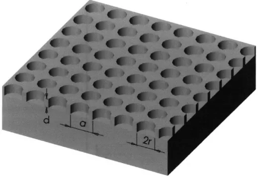
Numerous examples of photonic crystals occur in nature, such as in opal gemstones and Morpho butterflies, but it has only recently become possible to fabricate photonic crystals [6]. There are several different geometries and applications of photonic crystals. This thesis focuses on the fab-rication of a 2-dimensional photonic crystal geometry. An application of such a geometry is as a resonant thermal emitter which requires fabricating a silicon-on-sapphire (SOS) 2-dimensional photonic crystal structure. Another application is as a selective thermal emitter which requires fabricating a tungsten dimensional photonic crystal structure. Figure 2.2 illustrates a similar 2-dimensional photonic crystal structure to the one used to fabricate the resonant thermal emitter and selective thermal emitter. The periodicity, depth and diameter of the holes can be adjusted to achieve the desired electromagnetic wave propagation in the infrared region of the spectrum.
Figure 2.2: 2-dimensional photonic crystal structure where a is the periodicity, d is the depth and 2r is the diameter of the holes.
Chapter 2 Thermal Emission Devices
2.2
Resonant Thermal Emitter
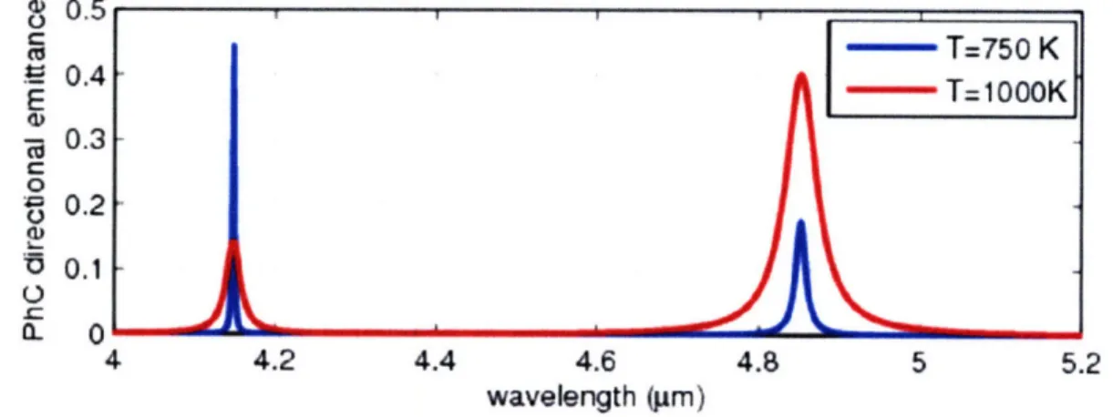
Through theory and simulation it has been shown that a 2-dimensional photonic crystal silicon slab exhibits narrow-band thermal emission peaks in the infrared region of the spectrum [1], [2]. The hole radius and free electron absorption can be adjusted to match the desired resonant fre-quency. Simulation of a 2-dimensional photonic crystal with a periodic square lattice of spatial period a and holes of radius r where r = 0.15a have exhibited several resonant peaks as shown in Fig. 2.3 [1], the structure of which is shown in Fig. 2.4. An equal amount of photons are emitted from the top side and bottom, sapphire, side of the 2-dimensional silicon on sapphire photonic crystal. Therefore it must be noted that the value of emittance shown in Fig. 2.3 is for only one side. There are many possible applications where it would be useful to be able to switch on or off the emission of radiation by simply changing the temperature of a substrate, including IR sensing, detection (enhanced bolometer) and light generation. This thesis focused on the development of a fabrication process for this novel structure.
C0 E o C 0 . 0. •0. CL 4 4.2 4.4 4.6 4.8 5 5.2 wavelength (pm)
Figure 2.3: Simulated 2-dimensional silicon photonic crystal slab with 1 tm periodicity and 400 nm
diame-ter holes displaying anomalous emittance (non-blackbody) and thermal radiation intensity at 750 K and 1000 K. Adapted from [1].
Chapter 2 Thermal Emission Devices
T
.
",appnire
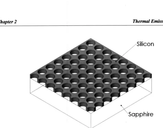
Figure 2.4: Resonant thermal emitter 2-dimensional silicon-on-sapphire photonic crystal structure.
2.3
Selective Thermal Emitter
A thermophotovoltaic converter is a static energy conversion device that converts heat into pho-tons and then into electricity. The idea of a TPV system was first proposed at MIT around 1956 [7], [8]. It is only now becoming possible, due to advances in material science and fabrication techniques, for TPV systems to reach an efficiency which is competitive in certain applications with other electrical energy conversion devices.
In a basic TPV system there are three main components, a high temperature source, an emitter and a photovoltaic (PV) diode. The high temperature source is in the range of 1000 -2000 K and is directly coupled to the emitter which emits photons in the infrared region of the spectrum. A photovoltaic diode converts incident photons above a certain minimum energy level, the band-gap energy, into electricity. Currently, due to economic reasons, gallium antimonide (GaSb) is the PV diode of choice in most TPV systems. GaSb has a band-gap of 0.78 eV which is less than that
-22
-Thermal Emission Devices Chapter 2
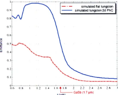
of silicon, 1.12 eV, but still only converts a relatively small amount of the radiated spectrum, wavelengths shorter than 1.7 pm, into electricity. To increase the efficiency of the GaSb PV diode a selective thermal emitter is used to supress radiation below the band-gap, wavelengths longer than 1.7 pm, from reaching the PV diode. A selective thermal emitter which offers the possibility of significantly improving TPV efficiency is the 2-dimensional tungsten photonic crystal struc-ture, the emittance and structure of which is shown in Fig. 2.5 [1] and Fig. 2.6 respectively. The reason for the difference between the emittance of the two structures is that the cavities in the selective thermal emitter rely on multiple resonances with relatively low Q factor to enhance broadband emission whereas the cavities in the resonant thermal emitter rely on isolated reso-nances to enhance narrow band emission. As mentioned previously, this structure has already been fabricated but based on the fabrication process developed in this thesis there is potential to achieve improved dimensional control and uniformity in the fabrication method of the selective thermal emitter which has the potential of increased TPV performance.
4) C E w O, S* 8 I I 14 1,6 t 1,8 2 2.2 2 4 2. 2.1 t A .(M.) GaSb (1 l rm)
Figure 2.5: Simulated normal emittance of flat tungsten and a 2-dimensional tungsten photonic crystal structure (1 pm periodicity, 800 nm hole diameter and infinite hole depth). Adapted from [1].
Thermal Emission Devices
Chapter 2 Thermal Emission Devices
Figure 2.6: Selective thermal emitter 2-dimensional tungsten photonic crystal structure.
-Chapter 3
Resonant Thermal Emitter Fabrication Technology
The goal of this chapter is to describe the main technologies used in the fabrication of the reso-nant thermal emitter discussed in Chapter 2, specifically the 2-dimensional silicon-on-sapphire (SOS) photonic crystal structure. Chapter 4 then examines the specific materials, processes and parameters which were used to implement the fabrication technologies discussed in this chapter. The chapter consists of six sections, each of which gives an in-depth description of a specific fabrication technology which was used. The first section examines chemical vapour deposition (CVD) which is used to deposit silicon dioxide on the surface of a substrate. Spin coating, another deposition technique, is examined in the second section and is used to coat the substrate with polymers of anti-reflection coating (ARC) and photoresist (PR). The third section discuses inter-ference lithography which is used to form the desired grid pattern of holes in the PR. The next section analyzes the operation of ARC's which are used to prevent the unwanted exposure of the PR. The penultimate section investigates the characteristics of PR which is the photosensitive material used as the initial mask layer. Finally, the transfer of the pattern of holes from the PR into the other layers in the stack by reactive ion etching (RIE) is studied in section six. Most of the technologies discussed are commonly used in microfabrication and although all the technolo-gies were used in this case to fabricate a resonant thermal emitter in SOS they could also be used to fabricate many other devices.
Resonant Thermal Emitter Fabrication Technology
3.1
Chemical Vapor Deposition
CVD is a method of material synthesis in which the constituents of a vapor phase react to form a
solid film at the surface of a substrate [11]. There are numerous different CVD techniques, most of which can be distinguished according to the form of energy that is supplied to chemically acti-vate the process. The original technique developed was atmospheric pressure CVD (APCVD); in which film deposition takes place on substrates which are heated using an inductively coupled graphite susceptor at a pressure of 760 Torr. Plasma-enhanced CVD (PECVD) is a technique involving the application of sufficiently high voltages at low pressure, 10 mTorr - 10 Torr, to cause 'breakdown' of the gas and a glow discharge plasma, consisting of ions, electrons and elec-tronically excited species, to appear and allows for low temperature deposition to take place [10]. PECVD has been used since the 1970's to deposit silicon nitride films for passivation layers to encapsulate integrated circuits and now is used to deposit thin films in the microfabrication of many devices such as transistors, photovoltaics and displays.
There are three fundamental stages of the PECVD process, as shown in Fig. 3.1. The first stage is the chemical activation of a gas molecule through electron impact causing dissociation into neu-tral radicals. This is achieved by an externally applied electrical field which causes plasma elec-trons, which are relatively light and easily accelerated, and ions, which are relatively heavy and therefore slower and less energetic. Due to the relatively large mass difference between the elec-trons and the gas molecules, low energy elecelec-trons do not lose much energy in collisions and col-lide elastically with the gas molecule. Therefore, plasma electrons accumulate energy in the elec-tric field until an electron has enough energy so that an inelastic collision takes place. In an ine-lastic collision the electron loses energy to the gas molecule, which can electronically excite the
-26 -Chapter 3
gas or cause it to dissociate or ionize. The energy required to cause ionization is much greater than that required for dissociation because the strong Coulombic forces to produce an ion and electron pair is much greater than that required to form two neutral fragments. Therefore, the density of ions in the plasma is much less than the density of radicals. Although only approxi-mately one part per million of the gas consists of electrons and ions they sustain the most visible part of the process, the glow discharge.
Electron *
SRadical*
Gas1. Chemical
MoleculeActivation
Radical•Q2.
Transport
3.
Bonding
Film Surface
Figure 3.1: The three basic stages of the PECVD process: 1. chemical activation by electron impact, 2. transport of the activated species to the film surface and 3. bonding to the film surface.
The second stage in PECVD is the transport of the radical species to the substrate surface. In most PECVD systems the gas flow rates are so low that diffusion is the dominant transport mechanism of neutral radicals. Diffusion occurs mainly due to a concentration gradient between the radicals
generated in the plasma and their disappearance at the film surface. Radicals created in the plasma undergo many collisions before reaching the surface of the growing film. Most of the collisions are with the source gas, due to its abundance; when these collisions occur within one or two collisions there is an end to the chemical reaction between the radical and the gas, if there is a reaction at all. Although the probability of a radical colliding with another radical is small, the reaction product is usually reactive. If the process repeats, then the molecule continues to grow into a macromolecule, and then into a particle. The deposition of particles formed in the gas stream onto the surface of the film cause defects to occur in the film and determine to an impor-tant degree the properties of the film. However, it is possible to control the degree to which this undesirable process occurs by adjusting the variables of the PECVD system.
The third PECVD stage is the chemical reaction of the radicals arriving at the surface of the growing film. PECVD resembles plasma etching, explained in Section 3.6, differing mainly in the surface reaction outcome. In the case of plasma etching, the reaction produces volatile species that leave the surface. While in the case of PECVD, the reaction bonds at least part of the radical to the surface and sometimes causes volatile reaction products to form and escape. These chemi-cal reactions take place under unusual energetic conditions where the reaction is particularly af-fected by temperature and ion bombardment.
In a PECVD system there are many variables which can be adjusted to change the properties of the film deposition, such as deposition temperature, chamber pressure, gas flow rates, input gas concentrations and the electrical power promoting the reaction. These primary process parameters enable an enormous parameter space of operation and make the PECVD system very versatile for thin film deposition.
3.2
Spin Coating
It is possible to form a thin uniform organic film of ARC and PR on a flat substrate by centrifugal spinning. An excess of the desired film material is applied as a fluid to the substrate and then rapidly rotated which causes the fluid to flow radially outwards and the excess fluid to spin off the edges of the substrate. As the fluid thins evaporation of volatile constituents takes place which causes the concentration to increase and a solid film results. The speed and duration of spinning can be varied to obtain very uniform films of desired thickness. Spin coating is commonly em-ployed in the microfabrication of many devices, especially in the lithography stage, where an accurate thin uniform film with a thickness in the range of nanometers is required. There have been numerous studies performed on the spin coating process explaining the formation of the uniform film and the dependence of the formation on material parameters [12], [13], [14], [15].
Based on the two fundamental principles of fluid mechanics, conservation of mass and conserva-tion of momentum, it is possible to derive an equaconserva-tion for the thickness of a thin film formed by spin coating. First considering the conservation of mass, the continuity equation for fluid dynam-ics states that in steady state the rate at which mass enters a system is equal to the rate at which mass leaves. The continuity equation for a single-phase fluid is
Op
V
= (3.1)-+V•'py = 0 at
where p is the fluid density, t is the total spinning time and v is the velocity vector. The diver-gence of the velocity vector can be expressed in 3-dimensional cylindrical coordinates (r, 0, z)
1 0 180v 0v4
V
v =
(rv)
+ r--
+a--
=0
(3.2)
r Or r aO Oz
Therefore the continuity equation in cylindrical coordinates (r, 0, z) is
Op 1a 10 0
a + a(prv)
+ --
•(pv
0) +
a(pVZ)
= 0
(3.3)
at rOr r00 0z
Second, the conservation of momentum, a form of Newton's second law, for a continuous fluid relates the velocities, pressure and stresses and is given by
(0v
p -+v. Vv =-Vp+v.'r+pf (3.4)
at
The terms on the left hand side of (3.4) result from the inertia of the fluid where the term
at
v comes from the unsteady acceleration while the v - Vv term comes from the convective accelera-tion. Thef
term represents the body force which result mostly from gravity, g, but in certain applications takes into account other forces such as electromagnetic. The Vp and V - r terms represent the stresses in the fluid where Vp describes the pressure gradient and V -7r represents the viscous forces. Assuming that the fluid is Newtonian and incompressible then it is possible to state that r, a stress tensor, is given byw = p(3.5)
where A is the rate of deformation tensor which in the case of a Newtonian fluid is assumed to be independent of the t. Substituting (3.5) into (3.4) gives the equation of motion for a Newtonian fluid, which in vector representation is
-30-Resonant Thermal Emitter Fabrication Technology
Resonant Thermal Emitter Fabrication Technology
av
p -+v(dat Svv) = -Vp + pV 2v + pf (3.6)
This is known as Navier-Stokes equation for a Newtonian and incompressible fluid. It can also be stated in terms of cylindrical coordinates as
r component:
(aVr
aVr VOa r o 2 rpat + v, a-• +
+Vz
a(t r r rO r z ] (3.7)ap
1
a
d= + (rvd ) dr (dr tr dr & component: (•v advO vo av0 +vrvoat
ar
r a
r
1 a22 r r2 d02 2 adv rz O50 dv0a 1 a
-r [ r I(rvo) 1 o2vo r2 2o 2 av, r2ao a2vz +PI z component: (avz avz at +VDr1
02vz a2 z) + aO + az + Pgz r 2ao
2 dz2J
1 dp r aO(3.8)
+ vz z r dOdap
Oz (3.9) Chapter 3 + zj 2 + P91 8 vz
+ a (-r
ar ar
avz
)T
Chapter 3 Resonant Thermal Emitter Fabrication Technology /
C
Vrh
\z
d2v•4
1
-pW2r
PT"2Substrate
rFigure 3.2: Illustration of the spin coating process.
In the case of spin coating, Fig. 3.2 shows the coordinate system and variables of interest. Based on this coordinate system it is possible to make a number of assumptions to simplify the applica-tion of Navier-Stokes equaapplica-tion to spin coating. Beginning with the following assumpapplica-tions:
1. Axially symmetric laminar flow takes place. 2. The radial velocity dominates, v, >> vz.
apr.
3. Quasi-steady state has been reached so the velocity gradient, - in (3.7), can be
neg-lected.
4. The shear stress arising from the velocity gradient is much larger than the stresses arising from the variation of Vr in the radial direction so the terms pvr and Itr[ (rVr) in (3.7) can be disregarded.
-32
-pV 2 a 2Vr
5. The equilibrium between the centrifugal term, - , and the viscous resistance,Y aZ, in (3.9) causes a steady flow to be achieved. Based on the previous assumptions and the fact that vz is small, all the other terms in the equation can be neglected,
6. There is no radial gravitational component because the plane is horizontal.
7. The liquid layer is so thin that differences in gravitational potential have negligible ef-fects in distributing the liquid compared with the effect of centrifugal forces and vy is as-sumed to be small so (3.9) reduces to 0 = ap
az
8. The pressure distribution external to the film is uniform. 9. The impact of surface tension is insignificant.
The above assumptions allow the Navier-Stokes equations in cylindrical coordinates to be re-duced to -PVo 2 a2Vr Op r - - - (3.10) r aZ2 2 and 0 = - (3.11) az
Based on assumptions 2 and 9, it is valid to assume that pressure is the only stress exerted in the z
direction on the free surface and so the external pressure must be equal to the fluid pressure at the surface. It is shown by (3.11) that the pressure within the fluid is independent of z and based on assumption 8 the pressure is also independent of r. Therefore, the pressure is constant everywhere within the fluid and so (3.10) reduces to
-PVO2 az2 (3.12)
r zZ2
Assuming that the fluid moves as a rigid body in the 0 direction at the same rotational speed as the substrate, given by v0 = ro, then (3.12) becomes
S = --pto2r (3.13)
where w is the rotational speed in radians per second.
In order to solve for the film thickness, h = h(r,t), boundary conditions must be applied. At the substrate surface boundary with the fluid, z = 0, the fluid velocity is equal to that of the substrate and as there is no radial velocity in the solid so the first boundary condition is
vr = 0 at z = 0 (3.14)
The second boundary condition occurs at the surface of the fluid film, z = h, and relates to the shear stress balance where the shear stress in the fluid is
F = - (3.15)
az
Assuming that no shear stress is exerted on the fluid by the ambient gas, the second boundary condition is
OVr = 0 atz = h(r,t) (3.16)
az
In order to solve for the film thickness, h(r, t), an equation relating it to vr(z) is required. Based on the assumptions above the continuity equation, (3.3), becomes
-34
-Resonant Thermal Emitter Fabrication Technology
Resonant Thermal Emitter Fabrication Technology
-(rv) + = 0
r r az
Multiplying both sides of (3.17) by dz and integrating from 0 to h gives
(3.17)
h1 +
frl-r
o r ar
(rvr)dz +I
-dz = 0o Oz
It is possible to define the radial flow per unit length of circumference as
q
=
fv
dz
and the rate of change of thickness with time as
-t
= VrIz=hSubstituting (3.19) and (3.20) into (3.18) results in
1 0 Oh -(rq) + - = 0
r
Or
atReturning to (3.13), it is now possible to perform a double integral to obtain an expression v, as
1 1
vr = -1po2rz 2 -_po2rhz which means that
q = v dz = P 2 h
By substituting (3.23) into (3.21) the following differential equation is obtained
(3.18)
(3.19) (3.20) (3.21) (3.22) (3.23) Chapter 3Resonant Thermal Emitter Fabrication Technology
h 1
f
p2 \ o 2\ah
=
--
a
23
= -
2
h
(3.24)
at r r r3I 3y
After multiplying across by dt, diving across by h3 and integrating both sides, the solution for the film thickness is obtained as
ho
h(t) =(3.25)
1 + 4 2) 2 (3.25)
where the constant h0, independent of r, corresponds to the initial height, t = 0, of the fluid layer.
Based on (3.25) a number of observations of how the film thickness varies can be made. First, it must be noted that the film gets thinner as the angular speed increases. Second, if the fluid thick-ness is initially uniform over the entire substrate then it remains uniform during spinning and independent of the size of the substrate. Third, the fluid layer decreases by 3 dB in a time
1
4 hp2 ho2 (3.26)
from which it can be observed that the thicker the initial layer, the faster the fluid thins out. Fourth, for very thin films, h<<ho, the film thickness is independent of its initial condition,
h(t)= (/1 11 (3.27)
'74) _o tN(
It must be noted that evaporation must occur in the spin coating process in order for a solid film to form and this fact has been ignored in the analysis. However, assuming that the concentration of the fluid is uniform then evaporation will occur over the entire surface area causing the solids concentration to increase uniformly.
-36
3.3
Interference Lithography
Nanometer scale patterns of gratings and grids can be formed over a large area using a maskless lithography technique known as interference lithography (IL) [16]. The basic principle of IL is that two plane waves incident on a sample result in a standing wave pattern. This pattern is then imaged into a layer of photo sensitive material known as photoresist (PR).
I
2
Figure 3.3: In interference lithography two plane waves interfere to form a pattern in photoresist. Adapted from [17].
The intensity of the standing wave pattern which result from the interaction of two plane waves of equal incident intensity is
Resonant Thermal Emitter Fabrication Technology Chapter 3
I
=
41
0
sin
2(!x)
(3.28)
where I is the total intensity, Io is the incident intensity from each plane wave, x is the position along the sample and p is the period of the of the standing wave pattern which is given by
A
p = 2sin(O) (3.29)
2sin(8)
where 2 is the wavelength of the incident waveform and 0 is the angel of incidence [19]. It is possible to change the period of the standing wave pattern and thus the period of the pattern formed in the photoresist by changing the angle of incidence. However, the minimum period that can be achieved is 2 which is usually constant because the wavelength of the source is normally fixed.
The exposure dose, DE, controls the linewidth of the pattern which forms and is obtained by the multiplying the intensity, I, by the exposure time t.
DE = It (3.30)
A 2-dimensional grid can be patterned by two orthogonal exposure doses, DEl and DE2.The
pat-tern which forms as a result of the two exposures is given by the sum of the individual exposures doses
DET= DEl + DE2= 410 1sin2 (-x) t1 + 4o102sin2 (-Y) t2 (3.31)
P1
P2
where DET is the total exposure dose, Io01 and 102 are the incident intensity from each plane wave during the first and second exposure respectively, t. and t2 are the duration of the first and
second exposures respectively, and P, and P2 are the respective periods. In most practical cases the wavelength and incident irradiation are uncontrollable. However, an arbitrary grid pattern can
-38-Resonant Thermal Emitter Fabrication Technology
be created by adjusting the angel of incidence and the duration of each exposure resulting in dif-ferent periods and linewidths respectively. In the case of a square grid pattern the periods and exposure times are set to be equal to each other for both exposures, P, = P2 = p and t = t2 = t,
so (3.31) can be simplified to
DET
=
4ot
(sin2
(
+ sin2
y
(3.32)Figure 3.4 shows the 2-dimensional standing wave pattern which results when the term in brack-ets in (3.32) is plotted, specifically the function sin2 ( x + sin2 y) is plotted for the case p=l.
a
Figure 3.4: MATLAB plot of the function: sin2(7rx) + sin2(7ry).
Resonant Thermal Emitter Fabrication Technology Chapter 3
3.3.1 Pattern Formation
Patterns are formed in PR when part of the applied dose is greater than the clearing dose, Dc, which is the specific minimum value required to change the solubility of the PR. As the value of Dc is constant, in order to change the size of the patterned features the exposure time must be adjusted. PR's will be further examined in Section 3.5 but it is worth noting that there are basical-ly two types of PR, negative and positive; in the case of negative resist the part which experiences
a dose greater than Dc becomes insoluble in PR developer whereas the opposite occurs in positive PR.
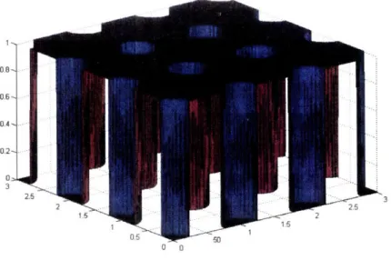
As shown in the Section 3.3, the exposure dose for a square grid is given by (3.32). This equation proves that the exposure dose is proportional to the duration of the exposure and that it is spatially variable, as shown in Fig. 3.4. The shape of the feature is set by scaling the graph shown in Fig. 3.4 to represent the exposure dose and then taking a cross-section at Dc. In the case of a high-contrast negative resist, rods form when Dc is greater than 50% of the maximum value of the exposure dose whereas holes occur when the dose is less than 50% of the maximum value. Figure 3.5 shows the rods which result from a relatively small exposure dose. Figure 3.6 shows the square shaped holes which form when the Dc coincides with the saddle point of the exposure dose. The holes which form when the exposure dose is increased so that Dc occurs at 25% of the maximum value of the exposure dose is shown in Fig. 3.7. In the case of positive resist the in-verse of these features would occur for the same conditions mentioned above.
-40
-Resonant Thermal Emitter Fabrication Technology Chapter 3
Resonant Thermal Emitter Fabrication Technology
U 0
Figure 3.5: MATLAB plot of the rods which of the maximum value of the exposure dose.
08 0.6- 04- 0.2-02ý 3
form in negative resist when the clearing dose occurs at 75%
u 0
Figure 3.6: MATLAB plot of the square holes which form in negative at 50% of the maximum value of the exposure dose.
resist when the clearing dose occurs
Chapter 3
Chapter 3 Resonant Thermal Emitter Fabrication Technology 1. -~ 0.6 0A4- 0.2-023 3, 0 0
Figure 3.7: MATLAB plot of the holes which form in negative resist when the clearing dose occurs at 25%
of the maximum value of the exposure dose.
3.3.2 Lloyd's Mirror Interference Lithography
There are various methods by which interference lithography can be implemented each of which has its own unique characteristics. One of the simplest methods is Lloyd's mirror IL which was developed in the nineteenth century and involves the use of a broad beam of light and a mirror to enable the reflection of part of the beam onto itself thus creating an interference pattern [16]. Figure 3.8 shows how in a Lloyd's mirror set-up some of the incident light is reflected off a mir-ror, which is at 90 to the substrate, resulting in two incident beams on the substrate with the same angle of incidence. As mentioned previously the angle of incidence, 0, of the beams is related to the period, p, of the interference pattern by
-42
-Resonant Thermal Emitter Fabrication Technology Chapter 3 r-0.8 0.6• 0,4• 0.2• O=
P = 2sin() (3.33)
2sin(0)
Therefore, by rotating the mirror/substrate assembly around the centre point it is possible to change the period of the pattern.
Mirror
Incident Light
rrate
Figure 3.8: The essential components of a Lloyd's mirror set-up. Adapted from [17].
There are many advantages of the Lloyd's mirror IL system over other IL systems including ease of use and the fact that it is relatively inexpensive. Another advantage is it's insensitivity to vibra-tions due to the fact that the mirror is in physical contact with the sample and so there is just a single beam for most of the optical path. Another advantage is that precise alignment does not have to be performed in order to change the period of the pattern, the mirror/substrate assembly simply needs to be rotated. However, there are a few disadvantages of the Lloyd's mirror IL system which are primarily a result of the mirror. Dust particles and irregularities in the mirror surface result in scattering and phase variations of the reflected beam which reduces the linearity of the grating. Also, the difference in optical path length due to the fact that the light reflects off the mirror and the fact that the mirror can drift from being perfectly normal to the substrate re-sults in reduced contrast between the interference fringes [20].
Resonant Thermal Emitter Fabrication Technology Chapter 3
Chaper Resnan ThrmalEmiter abrcaton Tchnlog
HeCd Laser
X-325nm
mirror
rotation
stage
1i·.
spatial
iflter
substrate
L
2 meter
expanslon
Figure 3.9: Illustration of the Lloyd's mirror interference lithography system. Adapted from [20].
Figure 3.9 illustrates the top view of a Lloyd's mirror IL system consisting of a 325 nm helium cadmium (HeCd) laser. Mirrors are used to direct the laser beam from the output of the laser to the spatial filter and to align the beam with the centre of the substrate/mirror assembly. The spa-tial filter is used to eliminate high frequency noise from the beam and results in a Gaussian beam whose intensity distribution is
(-2r2 (3.34)
1(r) = Ioe 0)(
where 10 is the intensity at the centre of the beam, r is the radial position from the centre of the beam and &o0 is the beam waist [19]. A plot of the normalized Gaussian beam intensity is shown Fig. 3.10. The fact that the beam is Gaussian means that the incident irradiation varies over the sample. However, the beam travels approximately 2 meters from the spatial filter to the sample which causes it to expand so that at the sample the variation in intensity is not significant for the relatively small samples of interest. Also, the large distance between the spatial filter and the sample allows the radius of the beam diameter to increase which results in the beam more closely
-44
-Resonant Thermal Emitter Fabrication Technology Chapter 3
approximating a plane wave at the substrate. However, a side effect of increasing the distance is that the intensity of the beam at the sample decreases and so a longer exposure time is required to obtain the same dose in the PR. Therefore, the choice of distance between the spatial filter and the sample is a tradeoff between pattern fidelity and exposure area versus exposure time.
I
0.9 0.8 0.7 0.6 0.5 0.4 0.3 0.2 0.1 0 0.2 0.4 0.6 0.8 1 1.2 1.4 1.6 1.8Normalized Radius (roo).
Figure 3.10: Normalized Gaussian beam intensity output from the spatial filter in the Lloyd's mirror IL system where r is the radial position from the centre of the beam and co is the beam waist.
The optical configuration at the substrate/mirror stage in the Lloyd's mirror IL system has a ma-jor impact on the performance of the system. An aluminium mirror is used because it exhibits relatively constant reflectivity over the range of angles of interest and exhibits very high reflectiv-ity at 325 nm. Also, the mirror is relatively large, 5 inches by 5 inches, in order to avoid edge effects as a result of scattering from the mirror. The axis of rotation of the stage is set to the point at which the substrate and mirror intersect so that by simply adjusting the angle of the stage the spatial period of the grating can be changed. The optical axis of the incident beam is also set to
Resonant Thermal Emitter Fabrication Technology Chapter 3
the point where the substrate and mirror intersect so that if the period of the grating is changed no optical alignment is necessary.
It is possible to form arbitrary patterns using the Lloyd's mirror IL system by performing multiple exposures at different angles and durations. As noted previously, to form a grid two orthogonal exposures must be performed for the same duration. It must be stated that the smallest feature which can be patterned using the Lloyd's mirror set-up described above is half the wavelength of the incident light. An in-depth analysis of the Lloyd's mirror IL system is given in [20].
3.4
Anti-Reflection Coating
ARC's are used in numerous applications to reduce the reflection of the incident light. In the case of Lloyd's mirror IL exposures, a standing wave normal to the surface of the substrate occurs due to the interference between the vertical component of the incident light and the reflection of light from the layers underneath the resist. The vertical standing wave causes unwanted patterning of the walls of the PR which reduces the repeatability of the process and causes problems in the pattern transfer stage. However, it is possible to reduce the magnitude of the vertical standing wave by adding a layer of ARC between the PR and the substrate. The ARC layer uses a combi-nation of both absorption and interference to reduce the vertical standing wave. The two impor-tant characteristics of the ARC layer are its thickness and index of refraction.
-46
Resonant Thermal Emitter Fabrication Technology Incident Light
Reflected
Light So Fis o\t l Kpa 0 Vertical ComponentFigure 3.11: The incident and reflected light decomposed into a horizontal and vertical component.
Figure 3.11 shows how the incident and reflected light can be decomposed into a horizontal and vertical component. The period of the horizontal standing wave determines the period of the grat-ing. While the period of the vertical standing wave, Pv, determines the period of the unwanted vertical pattern in the side walls of the PR and is given by
A
PV = 2ncos(O) (3.35)
where A is the wavelength of the light, 9 and the angle of incidence and n is the refractive index of the PR [16].
3.4.1 Index of Refraction
The magnitude of the vertical standing wave is highly dependent on the index of refraction of the ARC, NARc .The index of refraction is complex and can be represented in cartesian coordinates
as
NARC = nARC + jkARc (3.36) where nARC is the real part of the index of refraction which accounts for refraction and kARc is the imaginary part of index of refraction and accounts for absorption. The relation between NARC and the refractive index of the PR, NPR, and the absorption of the ARC have a significant impact on the vertical standing wave and will be examined in this section.
In order for a uniform exposure to occur throughout the PR NPR must have very low absorption and so NPR is mostly real. In the case of index matching NARc and NPR, it is valid to assume that they are both real and reduce to nARc and nPR respectively. The equation for reflection, R, for two semi-infinite layers with real refraction indices is
R = [nARC - nPR 2 (3.37)
tnARC + nPRI
which will evaluate to zero when the ARC and PR are perfectly matched [19]. However, in reality the layers are of finite thickness and there is a substrate below the ARC. Therefore, if nARc and nPR are equal then they appear as one layer and any reflected light from the substrate will also reflect back into the PR. Therefore, index matching of the PR and ARC is highly undesirable.
The absorption of the ARC is very significant and if it is high then it will reduce the magnitude of the light traveling through the ARC. However, the light must first get coupled into the ARC. Considering again the case of semi-infinite layers of ARC and PR but this time taking into ac-count the absorption term, the reflection, R, is given by
-48
Resonant Thermal Emitter Fabrication Technology
R
=
(nARC-
nPR)2(kARc
-kpR)
2R = + (3.3 8)
(nARC + nPR)2 + (kARc + kpR)2 (nARC + nPR)2 + (kARc + kpR) 2
which has been separated to illustrate the effects of the real and imaginary components of the index of refraction [19]. Therefore, the total reflection is dependent on the mismatch between the real parts and also the imaginary parts of the refractive indices of the two materials. Thus, it is possible for an ARC to cause high reflection as a result of a large mismatch in the absorption of the ARC and PR. However, in reality a specific ARC is chosen not based on its index of refrac-tion but rather on the processing steps which occur after lithography.
3.4.2 Thickness Calculation
It is quite straightforward to solve for the reflection in the case of two semi-infinite layers, equa-tion (3.38). However, when fabricating devices there are usually multiple metal and dielectric layers of varying thickness in which case the calculation of reflection becomes quite complex [19]. A simulation based on a transmission line model was developed in [16]. It plots the reflec-tion back into the PR as a funcreflec-tion of the ARC thickness for a stack of thin film layers. Once the refractive indices of all the materials in the stack are known and the thickness of each layer in the stack except the ARC has been determined it is possible to calculate the optimum thickness of the ARC to minimize the reflection back into the PR. This is discussed further in Section 4.1.2.
Resonant Thermal Emitter Fabrication Technology
3.5
Photoresists
As mentioned in Section 3.3.1, PR's are polymers in which the solubility changes as a result of the applied dose. The development of PR's has been pioneered by the semiconductor industry in order to decrease the feature size of integrated circuits but there are many other applications in which PR's are used [21]. In each application there are many factors which determine the suita-bility of a specific PR, including the properties of the PR itself. The most important photoresist properties include contrast, transparency, adhesion and dose. The contrast of a PR is a measure of the how closely the PR exposure matches a binary response. A high contrast PR is one which transitions between exposed and unexposed as a result of quite a small difference in exposure dose.
It is desirable for the PR to be transparent enough so that the lower portion of the resist expe-riences the same dose as the upper portion of the resist. However, some absorption must occur within the PR in order for exposure to take place. Therefore, a trade-off must be made between uniformity of the pattern throughout the resist and the absorption which is essential for exposure. The need for transparency has been one of the major areas of PR research in the semiconductor industry.
Adhesion is sometimes a problem with PR's because most of them do not adhere well to hydro-philic surfaces such as silicon dioxide, so an adhesion promoter such as hexamethyldisilizane (HMDS) must be used. By spinning HMDS on the surface, a monolayer forms which converts the surface from hydrophilic to hydrophobic, which most PR readily adheres to.
-50 -Chapter 3
3.5.1 Dose
The dose is commonly calculated by multiplying the exposure time, tE, by the intensity of the incident radiation, I,, from the laser beam (3.39). However, in the case of the Lloyd's mirror IL system this method is only valid for a specific grating period and resist stack. Therefore, a more detailed calculation must be performed in order for it to be possible to calculate the dose required to form a grating of any period.
D = IltE (3.39)
The dose calculated by multiplying the exposure time by the intensity of the incident radiation is actually is not the dose that the PR experiences. It is the incident dose, DI, and is usually much higher than the actual exposure dose in the PR, DE. To calculate DE the reflectivity of both the top and bottom surfaces of the resist and the angle of the incidence of D, must be taken into ac-count. The reflection off the top surface of the PR, RT, determines the amount of incident light that gets coupled into the PR. DE is directly proportional to 1 - RT and so it is desirable to mi-nimize the surface reflection in order to reduce the required exposure time. The reflection from the layers beneath the PR, RB, is directly related to DE by 1 + RB and as discussed in Section 3.4 this reflection is undesirable and a layer of ARC is usually used to minimize its effect. The angle of incidence of the beam, 0, the same angle defined in Fig. 3.8, has an impact on RT and RB. Also, as the angle of incidence increases the cross-section of the substrate in the beam deceases so the density of incident light on the surface of the PR decreases and so DE is directly
propor-tional to cos(0)DI. By taking all the above observations into account it is possible to formulate an
equation for DE such that
![Figure 3.9: Illustration of the Lloyd's mirror interference lithography system. Adapted from [20].](https://thumb-eu.123doks.com/thumbv2/123doknet/13881039.446765/44.918.132.774.192.498/figure-illustration-lloyd-s-mirror-interference-lithography-adapted.webp)
