360° domain walls: stability, magnetic
field and electric current effects
The MIT Faculty has made this article openly available.
Please share
how this access benefits you. Your story matters.
Citation
Zhang, Jinshuo et al. “360° Domain Walls: Stability, Magnetic Field
and Electric Current Effects.” New Journal of Physics 18.5 (2016):
53028. © 2016 IOP Publishing Ltd and Deutsche Physikalische
Gesellschaft
As Published
http://dx.doi.org/10.1088/1367-2630/18/5/053028
Publisher
IOP Publishing
Version
Final published version
Citable link
http://hdl.handle.net/1721.1/105358
Terms of Use
Creative Commons Attribution 3.0 Unported licence
This content has been downloaded from IOPscience. Please scroll down to see the full text.
Download details: IP Address: 18.51.1.88
This content was downloaded on 06/10/2016 at 19:09
Please note that terms and conditions apply.
You may also be interested in:
Driving large-velocity propagation of ferromagnetic /2 domain walls in nanostripes of cubic-anisotropy materials
Andrzej Janutka, Przemysaw Gawroski and Pawe S Ruszaa
Current-induced domain wall motion in Ni80Fe20 nanowires with low depinning fields Grégory Malinowski, Andreas Lörincz, Stephen Krzyk et al.
Domain wall dynamics of periodic magnetic domain patterns in Co2MnGe-Heusler microstripes K Gross, K Westerholt and H Zabel
Multiple switching fields and domain wall pinning M Brands and G Dumpich
Magnetism in curved geometries
Robert Streubel, Peter Fischer, Florian Kronast et al.
Cascade-able spin torque logic gates with input–output isolation Dmitri E Nikonov, Sasikanth Manipatruni and Ian A Young
Current-induced domain wall motion in nanoscale ferromagnetic elements G Malinowski, O Boulle and M Kläui
360° domain walls: stability, magnetic field and electric current effects
View the table of contents for this issue, or go to the journal homepage for more 2016 New J. Phys. 18 053028
(http://iopscience.iop.org/1367-2630/18/5/053028)
New J. Phys. 18(2016) 053028 doi:10.1088/1367-2630/18/5/053028
PAPER
360° domain walls: stability, magnetic
field and electric current
effects
Jinshuo Zhang1
, Saima A Siddiqui2
, Pin Ho1
, Jean Anne Currivan-Incorvia2,3
, Larysa Tryputen1
, Enno Lage1 , David C Bono1
, Marc A Baldo2
and Caroline A Ross1,4
1 Department of Materials Science and Engineering, Massachusetts Institute of Technology, Cambridge, MA 02139, USA 2 Department of Electrical Engineering and Computer Science, Massachusetts Institute of Technology, Cambridge, MA 02139, USA 3 Department of Physics, Harvard University, Cambridge, MA 02138, USA
4 Author to whom any correspondence should be addressed.
E-mail:[email protected]
Keywords: spintronics, magnetic domain wall, anisotropic magnetoresistance, micromagnetic simulation Supplementary material for this article is availableonline
Abstract
The formation of 360° magnetic domain walls (360DWs) in Co and Ni
80Fe
20thin
film wires was
demonstrated experimentally for different wire widths, by successively injecting two 180° domain
walls
(180DWs) into the wire. For narrow wires (50 nm wide for Co), edge roughness prevented the
combination of the 180DWs into a 360DW, and for wide wires
(200 nm for Co) the 360DW was
unstable and annihilated spontaneously, but over an intermediate range of wire widths, reproducible
360DW formation occurred. The annihilation and dissociation of 360DWs was demonstrated by
applying a magnetic
field parallel to the wire, showing that annihilation fields were several times higher
than dissociation
fields in agreement with micromagnetic modeling. The annihilation of a 360DW by
current pulsing was demonstrated.
Magnetic domain walls(DWs) in narrow wires provide a data token for devices such as racetrack memory and logic gates[1–3]. DW devices maintain the traditional merits of magnetic data storage including non-volatility and high density, but offer new functionality including fully electrical operation by using spin torque transfer to manipulate the DWs and magnetoresistance to detect them. This can in principle enable faster switching speeds and lower energy consumption compared to DRAMs and other semiconductor devices[4]. Many proposed DW devices are made from nanowires containing 180DWs, where the orientation of magnetization rotates through 180° [5,6]. An essential requirement for DW devices is to be able to translate DWs within the device, which can be accomplished using a magneticfield or a current pulse due to spin transfer torque [7,8].
The 180DW in a wire with in-plane magnetization adopts a vortex or a transverse configuration, with transverse DWs favored in narrow or thin wires[6] as shown in the upper panel of figure1(a). Closely spaced 180DWs in a nanowire interact magnetostatically, and the attraction between two 180DWs of opposite core magnetization can lead to the formation of a metastable 360° domain wall (360DW), as shown in the lower panel offigure1(a). 360DWs are also known as 1D skyrmions [9], an example of a class of topologically protected structures which are under intense study due to their stability and device applications[10].
360DWs have been observed both in continuous ferromagneticfilms [11] and in ferromagnetic nanostructures such as thinfilm rings or ellipses [12–14]. The orientation of magnetization rotates through 360°, and due to the opposite sense of core magnetization in the two component 180DWs, magnetic flux closure reduces the strayfield around the 360DW in a thin film wire compared to that of a 180DW [15]. 360DWs are not expected to be translated by an appliedfield, but instead can be dissociated or annihilated. However,
micromagnetic simulations predict that a current can translate the 360DW via spin torque transfer[15]. Moreover, instead of Walker Breakdown as observed in 180DWs, a 360DW is predicted to undergo annihilation at a sufficiently high spin current density. Simulations predict that 360DWs of different chirality can be filtered OPEN ACCESS
RECEIVED
7 December 2015
REVISED
18 March 2016
ACCEPTED FOR PUBLICATION
29 April 2016
PUBLISHED
17 May 2016
Original content from this work may be used under the terms of theCreative Commons Attribution 3.0 licence.
Any further distribution of this work must maintain attribution to the author(s) and the title of the work, journal citation and DOI.
[16], and 360DWs have been proposed for use in magnetic sensors [17] and as an alternative to 180DWs in memory and logic.
360DWs in magnetic wires have been detected using magnetic force microscopy(MFM) [11], scanning electron microscopy(SEM) with polarization analysis [14], and anisotropic magnetoresistance (AMR) measurements[18–21], in which the formation of a 360DW results in a decrease of resistance. There has been considerable theoretical and modeling work on the behavior of 360DWs[22–24], but there have been no systematic experimental reports on the formation of 360DWs, their response to afield as a function of wire width, nor any observation of current-driven motion of a 360DW. In this article, wefirst demonstrate the formation and stability of 360DWs in specifically designed Co and Ni80Fe20nanostructures of different widths
with in-plane magnetization. We then demonstrate the effect of applied magneticfields or injected current pulses on 360DWs using AMR measurements for Ni80Fe20samples and MFM measurements for Co samples.
Ni80Fe20has a relatively large AMR response so that individual DWs can be detected in situ, but its low switching
field renders DWs vulnerable to perturbation by the stray field of an MFM tip. On the contrary, Co has a lower AMR but its higher switchingfield facilitates direct imaging of the stray field of DWs by MFM. Therefore studies of 360DWs in both NiFe and Co provide complementary information. We relate the experimental results to micromagnetic simulations.
The method used to generate a 360DW is similar to previous work[14]. The structures consist of a magnetic thinfilm wire in the shape of an arc, with width varying from 50 to 200 nm, connected to a round injection pad of 1μm diameter. The structures were made from a thin film stack of Ta (5 nm)/Ni80Fe20(10 nm)/Au (5 nm) or
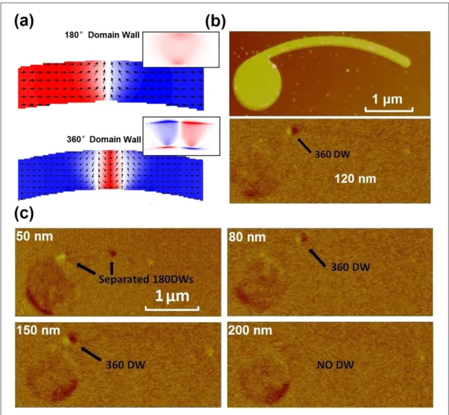
Ta(5 nm)/Co (10 nm)/Au (5 nm) which was deposited by magnetron sputtering (5 cm diameter target, 100 W, Figure 1.(a) Simulation of a transverse 180DW and a 360DW inside a Co arc, 10 nm thick and 120 nm wide. Arrows show
magnetization, red(positive) and blue (negative) indicate the component of magnetization along the wire length, the x-direction. Insets are the simulated z-component of the strayfield at a height of 3 nm above the surface of the sample. Blue and red represent up and down directions.(b) The upper AFM image shows a 120 nm wide Co wire and pad used to generate a 360DW, and the lower MFM image illustrates a 360DW in the wire.(c) MFM images of other Co samples with wire width of 50, 80, 150 and 200 nm.
2
and growth rates of 0.15–0.30 nm s−1for different materials) on a Si substrate with native oxide, at an Ar pressure of 1 mTorr and a base pressure better than 5×10⁻⁸Torr. A bilayer resist[25] consisting of 4%
polymethyl-methacrylate(PMMA) of thickness 30 nm and 2% hydrogen silsesquioxane (HSQ) of thickness 40 nm was spin coated on the magneticfilm then exposed using an Elionix F-125 e-beam lithography tool with a dose of 38 mC cm−2. The HSQ layer was developed using 4% NaCl+1% NaOH in water solution for 20 s, washed with DI water and carefully dried by a nitrogen blow gun. The underlying PMMA layer was then removed with O2plasma at a pressure of 6×10⁻³Torr at 90 W power for 2 min. Using these patterned bilayer
resists as an etch mask, the metalfilm was then etched using an Ar ion beam with a beam current of 10 mA and pressure of 2×10⁻⁴Torr. The etching was monitored using an end-point detector. Since the PMMA acts as a sacrificial layer, the resist stack could then be removed with hot 1165 solvent [MicroChem Corp.] and sonication after the ion beam etching. An AFM image of a typical structure is shown in the upper panel offigure1(b). For AMR measurements of Ni80Fe20samples, four electrodes made of Ta(7 nm)/Au (100 nm) were patterned using
liftoff over the pad-wire structure in a second lithography step to enable a four-point measurement of resistance. For MFM characterization, we used low moment magnetic tips(Bruker MESP-LM) in order to reduce the interaction between the sample and the strayfield of the tip. Lift height was set to 50 nm during the second MFM pass to ensure relatively small interaction between sample and tip as well as to obtain clear phase information. The scale for the MFM phase images shown in this paper is 3 .
Micromagnetic simulations were performed using the OOMMF package[26]. For Co the exchange constant
=
-A 10 5erg cm−1, saturation magnetizationM = 1000
s emu cm−3, a = 0.02, b = 0.03 and anisotropy
=
Ku 105erg cm−3with a random orientation for each cell to simulate a polycrystallinefilm. For NiFe the exchange constant wasA = 1.3 10-4erg cm−1, saturation magnetizationM = 800
s emu cm−3, anisotropy
=
Ku 0, a = 0.02 and b = 0.03. The length and thickness of the simulated wires were 10μm and 10 nm, respectively. The cell size was(5 nm)3in most simulations, though(2 nm)3cells were used for comparison: this predicted a criticalfield and a critical current for annihilation that were higher by about 15%, but the results were qualitatively the same.
We describefirst the formation and stability of 360DWs in Co arcs. In order to generate a 360DW, an in-planefield sequence was applied perpendicular to the arc.Hy= +3000 Oewas applied to fully saturate the magnetization and form thefirst 180DW with its core magnetized along +y at the center of the arc at
remanence.Hy= -300 Oewas then applied, afield sufficient to reverse the magnetization in the round pad but not high enough to reverse the magnetization in the arc due to its higher shape anisotropy. A second 180DW with opposite sense to thefirst 180DW was formed at the interface between the round pad and the arc. The two 180DWs combine to form a 360DW aided by their magnetostatic attraction[14]. AFM and MFM images of a Co sample of width 120 nm are shown infigure1(b). The dark and bright contrast observed at the center of the arc qualitatively resembles the calculated strayfield around the 360DW in figure1(a) and confirmed the presence of a 360DW.
Co samples with different arc widths of 50, 80, 120, 150 and 200 nm were tested to study the 360DW stability as a function of arc width. We expect TWs to be energetically preferable within the width range according to micromagnetic simulations in Co nanowires. The 80, 120 and 150 nm samples successfully formed a 360DW in the arc. In the sample with 50 nm wire width, two 180DWs of opposite sense were formed but remained separate in the arc without combining into a 360DW(the bright contrast originates from the second 180DW). This is attributed to pinning: the amplitude of line edge roughness is expected to be independent of wire width[25], but the resulting changes in wire width are proportionately larger for narrower wires. The length of a 180DW also decreases with decreasing wire width[2], making it more sensitive to high frequency edge roughness. These factors lead to stronger pinning of the 180DWs in narrower wires, which impedes their combination into a 360DW.
For the sample with wire width of 200 nm, no 360DW was observed. MFM images of the sample after applying the initial saturationfield ofHy= +3000 Oeshowed a 180DW with transverse configuration as illustrated by dark contrast at the arc center. This result shows that a 180DW could be formed but the second 180DW is assumed to annihilate thefirst one instead of forming a 360DW. The reduced influence of edge roughness may have enabled the second 180DW to approach thefirst at a higher velocity, which promotes annihilation.
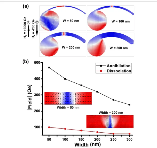
The experimental results for 360DW formation under transversefield cycling agree with the prediction of micromagnetic modeling,figure2(a), for Co arcs. Simulations were performed with the same field sequence of Hy=+3000 Oe followed by Hy=−200 Oe, for wire widths of 50, 100, 200 and 300 nm. The arc shape in the
model leads to edge roughness due to thefinite cell size. The 50 nm wide model wire was unable to form a 360DW because the second 180DW did not propagate far enough to combine with thefirst 180DW. The 100 and 200 nm arcs did produce 360DWs, but in the 300 nm wide model wire the 360DW spontaneously annihilated.
The effect of magneticfield on 360DWs was studied experimentally in both Ni80Fe20and Co samples and
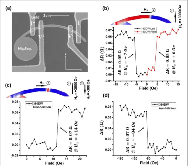
characterized by AMR and MFM, respectively. A SEM image of a Ni80Fe20sample is shown infigure3(a), which
3
was 200 nm wide and 10 nm thick. Vortex DWs are energetically favorable in this material and geometry compared to TWs, according to micromagnetic simulations. A small DC current was applied between the outer two electrodes and the voltage between the inner two electrodes was measured in order to obtain the resistance. This reference DC current was lower than 5μA, corresponding to an average current density of
< ´2 109A m−2in the arc, which was 0.001–0.01 times the current density reported to move a DW in Ni
80Fe20
nanowires[8,27–30]. Therefore the effect of the measurement current on the wall was neglected. As shown in the round dot line infigure3(b), a head-to head 180DW was formed by applying = +
Hy 3000 Oe,then afield in the +x direction was applied, starting from zero and increasing with a step size of 1 Oe. The resistance was measured after eachfield step. A change of D =R 0.055 0.005 Wwas observed at 5 Oe based on ten repeated measurements, indicating movement of the 180DW to the right, out of the area between the inner two electrodes. The increase of the resistance is due to the AMR effect from the 180DW: the resistance is lower at the DW because the magnetization is locally perpendicular to the electronflow. The AMR follows the relation
( ) ( ) r r r r q D = D -⎜ ⎟ ⎛ ⎝ ⎞ ⎠ H cos 1 3 1 av av 2
in whichD H is the change of resistivity and q is the angle between magnetization and electron flow [r( ) 31]. If a field was applied in the –x direction, a similar resistance jump of D =R 0.053 0.005Wwas observed at −6 Oe based on ten repeated measurements, shown in the square dot line in figure3(b). This indicated the 180DW moving to the left, out of the area between the inner two electrodes. Out of 20 total measurements, the resistance jump was very similar for eight and nine of the measurements forfields along +x and −x, respectively.
Figure 2.(a). Simulation of 360DW formation process in 10 nm thick Co arcs of different widths, with field applied transverse to arc. (b). Calculation of the critical annihilation and dissociation fields applied parallel to wire versus wire width in straight 10 nm thick Ni80Fe20wires based on micromagnetic simulations. Images of the remanent 360DWs at 50 and 300 nm width are superposed. For the 200, 250 and 300 nm wide wires, the initiation of the model led to energetically unfavorable TWs instead of VWs.
4
The other three tests gave either no resistance change or a change of »0.03 Wwhich may have indicated differences in the DW structure or location. Other groups have also shown DW AMR in large numbers of repeated tests[18]. We used the eight and nine measurements to calculateDR.
Afield sequence ofHy= +3000 Oefollowed byHy= -300 Oewas then used to form a 360DW in the 200 nm wide Ni80Fe20wire, followed by afield in the +x or −x direction as shown in figures3(c) and (d),
respectively. Infigure3(c), a resistance jump of D =R 0.078 0.007 Wbased on ten measurements was observed at Hx@ +14 Oe.The higher resistance change confirmed the presence of a 360DW instead of 180DW and the higher value of Hxrepresents the criticalfield to dissociate a 360DW, overcoming the
magnetostatic attraction between the two component 180DWs and separating them to form a reverse domain. In comparison, infigure3(d), a resistance jump of D =R 0.075 0.007 Wwas observed at Hx@ -84 Oe, much higher than the criticalfield in figure3(c). This represents the critical field to annihilate the 360DW, in which thefield compresses the 360DW, eventually eliminating it. The ratio of AMR change expected between a 180DW and a 360DW was calculated by exporting the magnetization distribution from OOMMF into MATLAB and determining the resistance based on equation(1). The AMR ratio wasDDR =1.46
R 360
180 for a Ni80Fe20nanowire withw=200 nm and =t 10 nm, similar to the experimental result ofDDR » WW =1.39 0.09
R
0.075 0.054
360
180 .
Simulations in Ni80Fe20nanowires were carried out to calculate the criticalfields for annihilation and
dissociation of a 360DW versus wire width,figure2(b). We first initiated a 360DW at the center of the wire, allowed it to relax, then applied afield in either the +x or −x direction along the wire to dissociate or annihilate the 360DW, respectively. We increased thefield from 0 with a step size of 10 Oe in order to find the critical value. As shown infigure2(b), the critical fields for annihilation and dissociation decreased by about 40% and 80%, respectively with an increase of wire width from 50 to 300 nm. The 360DW became less symmetrical as the width
Figure 3.(a) SEM image of Ni80Fe20sample with gold electrodes on top. A DC current less than 5μA is injected from I+to I−to measure the AMR.(b) AMR measurements indicating a 180DW being moved left or right by a field Hx. The sequence offields used to generate the wall then move it are shown with circled numbers, with negative Hxmoving the wall along the−x direction. (c) Schematic and model of thefield sequence to form and then dissociate a 360DW. AMR measurements indicate dissociation in a field applied in the+x direction. (d) AMR measurements indicate annihilation of the 360DW in a field applied in the −x direction.
5
increased, with the two component 180DWs tilting towards each other at one side of the wire, making the 360DW less stable. It has also been shown in[18] that the 360DW forms a much less stable vortex structure with increasing wire width.
For a model Ni80Fe20nanowire of width w=200 nm and thickness t=10 nm, the critical field to dissociate
a 360DW is Hx= +75 Oeand to annihilate it is Hx= -310 Oe.The modeling predicted much higher absolute values of the annihilation and dissociationfields than were measured experimentally, which may be a result of the zero temperature of the model and the lack of extrinsic defects that could initiate annihilation and dissociation. However, both model and experiment agree in showing annihilationfield several times larger in magnitude than dissociationfields.
The effect of a magneticfield on 360DWs in Co nanowires were examined using MFM. As shown in figure4(a), a 360DW was first formed in a Co sample with wire width of 80 nm by applyingHy= +3000 Oe thenHy= -300 Oe.Different magneticfields were applied in the +x direction to dissociate the 360DW. The 360DW was unchanged for Hx +125 Oe,but after the application of Hx= +150 Oe,the two component 180DWs moved apart forming a reverse domain. After the application of Hx= +200 Oe,the component 180DWs moved further such that the left-hand bright-contrast wall moved into the injection pad and the right dark-contrast wall moved to the end of the wire. The reversal of the wire is evident from the change in contrast from bright to dark at the tip of the wire, labeled by the black circles infigure4. A similar dissociation process was observed in a Co sample with 150 nm wire width,figure4(b), except that the field steps did not capture the presence of two separate 180DWs in the wire. In the 150 nm wide wire, dissociation occurred at afield between 125 and 150 Oe.
360DW annihilation in a Co sample was demonstrated by applying afield in the–xdirection. The samefield sequence as infigure4was applied initially to form a 360DW at the center of the arc. The MFM measurements are shown in the supplement(figure S1). The 360DW remained stable in the arc for -Hx500 Oe.The 360DW disappeared after applying afield of Hx= -700 Oe,but different from the dissociation results in figure4, the right-hand end of the wire retained its bright contrast before and after the annihilation. This proves that the magnetization direction remained the same in the arc, indicating annihilation instead of dissociation of the 360DW. Thefield for annihilation (−700 Oe) was also much larger than that for dissociation (+150 Oe) in the 150 nm wide Co wire, confirming the same trend as seen in the Ni80Fe20samples and in micromagnetic
simulations.
The effects of current on 360DWs were examined in 150 nm wide Co samples. Two electrodes were placed on top of the sample as shown infigure5(a), labeled I+and I−, and the conventional currentflowed from the right electrode to the left electrode. Figure5(b) is an MFM image of the sample initiated with a 360DW at the arc center. Current pulses of+2 V, +4 V or +6 V amplitude and 200 ns duration were then injected into the sample, corresponding to current densities of approximately 1.2, 2.4 or3.6 ´ 1012A m−2respectively in the arc,
averaged over the Ta/Co/Au stack. A delay of 3 s was inserted between each pulse to minimize Joule heating [32]. From MFM imaging there was no observed effect of current pulses with amplitude of 2 V. Figure5(c) shows the 360DW after two pulses of 4 V, which moved∼200 nm to the right, indicating a small current-driven 360DW motion. We did not see any further translation after two additional pulses of 4 V, but after ten additional
Figure 4.(a) A series of MFM images of a 360DW in a Co wire with width of 80 nm after application of different fields in the +x direction, showing separation into two 180DWs at+150 Oe and movement of the walls out of the wire at +200 Oe; (b) A series of MFM images of a 360DW in a Co wire with width of 150 nm after application of differentfields in the +x direction. The wall was dissociated and the two 180DWs moved out of the wire between 125 and 150 Oe. In both samples dissociation is evident from the change of contrast at the tip of the wire from light in thefirst panel to dark (black circle).
6
pulses of 4 V the 360DW disappeared as shown infigure5(d). Since the current is limited to the region of the arc between the two electrodes, the current-driven 360DW will not be able to move further than the electrode. Moreover, from our tests the phase contrast of a 360DW can still be observed at 150 nm lift height, which means that even if the 360DW is beneath the arc, we should still be able to see the phase contrast. As shown in
figure5(d), MFM did not reveal the 360DW remaining under the Au contact, implying that the 360DW was annihilated.
An estimation of the temperature increase from Joule heating at the end of a current pulse was made based on the calculation in[33]: ( ) ( ) pm s r m = ⎛ ⎝ ⎜ ⎞ ⎠ ⎟ T t whJ C t w ln 4 , 2 G s w s s s G 2
where widthw=300 nm, thicknessh=20 nm(including the seeding layer and capping layer), current densityJ=3.3´1012A m−2, thermal conductivitym ( )Si =8.8´10
-s 5m
2
s−1, electrical conductivity ( )
sw Co =107(Ω m)−1, material density r = 8900s kg m−3, heat capacityCs=400 J(kg K)−1, pulse duration =
t 200 ns andwG=w 2/ = 150 nm.By substituting the parameters for the 4 V pulse, an approximate maximum temperature increase of 36 K was obtained.
Previous simulation results[15] predicted that in a smooth-edged nanowire with zero anisotropy, a spin current will translate a 360DW, and at high enough spin current density will annihilate it. However, our experiments showed annihilation after only a small translation. The limited current-driven motion of the 360DW is attributed to the anisotropy from Co and extrinsic pinning from edge roughness. This was confirmed by measurements of current-driven motion of 180DWs in the same sample. Ten identical 200 ns current pulses were injected at voltages of+2 to +6 V (the highest voltage led to damage to the sample), but the 180DW was not translated. This suggests that DWs are pinned in the Co nanowires[34], and the current therefore annihilated the 360DW without moving it.
To assess the role of edge roughness, simulations(at zero temperature) were performed for Co nanowires with the same random anisotropy as described above as well as with an edge roughness amplitude3% of the average wire width, produced by removing cells from the side of the wire randomly. Both 360DWs and 180DWs were only able to move by< 100 nm when a current density of5.3´1012A m−2was applied. On increasing the
current density to7.1´1012A m−2, the 180DW translated further while the 360DW was annihilated after an
initial »100 nm motion. This shows the importance of the edge properties on the motion of the DWs.
The experimental results show that current pulses provided an effective method for annihilating the 360DW. It required−700 Oe to annihilate a 360DW in the 80 nm wide Co sample but only +150 Oe to move a 180DW. For the current pulsing, annihilation of the 360DW occurred at 4 V pulse amplitude but moving a 180DW required at least 6 V. The joule heating during current pulsing may contribute to destabilizing the wall, but the temperature decreased too quickly to enable an accurate measurement[32]. We estimated above that the
Figure 5.(a) AFM of Co sample with wire width 150 nm with gold electrodes on top, with I−and I+indicating the direction of current flow. (b) MFM of the sample after initializing a 360DW. (c) MFM of the sample after injecting two current pulses with +4 V amplitude and 200 ns duration showing a small translation of the 360DW.(d) MFM of the sample after injecting ten more current pulses with +4 V amplitude and 200 ns duration, showing annihilation of the 360DW.
7
temperature increase would be∼36 K based on the results in [33,35], which is also consistent with a measurement based on resistance change[36].
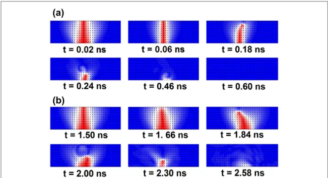
The modeling illustrates the different 360DW annihilation mechanism between using current pulses and using externalfield, making current pulses particularly effective in 360DW annihilation. Figures6(a) and (b) show snapshots of the simulated 360DW annihilation processes driven byfield and current in a 100 nm wide and 10 nm thick wire, using the same parameters as infigure2. A cell size of(2 nm)3was used in this set of simulations. Infigure6the 360DW develops a trapezoidal shape with the narrower side at the bottom of the figure. In the field-driven annihilation process, the field pushes the two component 180DWs together and when they are close enough the 360DW is annihilated starting from its narrower edge. On the contrary, in the current-driven annihilation process, the current translates the 360DW, which moves with an oscillatory motion and becomes unstable, eventually closing up from the narrower edge. During the annihilation process, the exchange energy provides a barrier for annihilation. At the critical annihilationfield of 320 Oe, the maximum exchange energy was 1.24´10-17 J,while at the critical annihilation spin current velocity of u=180 m s−1 (corresponding to a current density of =J 6.3´1012A m−2), the maximum exchange energy was only
´
-0.78 10 17J.The difference points to the instability of the 360DW under current as a contributing factor to the annihilation process.
In summary, 360DWs were formed in both Ni80Fe20and Co wires with a range of widths. 360DW
dissociation and annihilation were experimentally observed by AMR measurements in Ni80Fe20and by MFM
measurements in Co nanowires, and the criticalfields were determined. The experimental results were compared with micromagnetic simulations, both of which showed thatfield-driven annihilation requires several times largerfield than field-driven dissociation, though the magnitude of the critical fields was higher in the simulations. The effects of current on 360DWs in Co were examined using MFM. Current produced a small translation of the 360DW then led to its annihilation at2.2´1012A m−2, a current smaller than that required
to translate a 180DW in a Co nanowire of the same width. The highfields required for translation are attributed to edge pinning in the Co, but the relatively low current required for annihilation is consistent with the lower energy barrier for current-driven annihilation compared tofield-driven annihilation predicted by
micromagnetic modeling. The modeling also predicts a different annihilation mechanism for current andfield. These results provide experimental evidence for the formation and manipulation of 360DWs, which are important in the study of memory and logic devices based on both 180DWs and 360DWs.
Acknowledgments
This work was supported by the NSF under award ECCS 1101798. Shared facilities of the MIT NanoStructures Laboratory and Center for Materials Science and Engineering(NSF DMR1419807) were used.
Figure 6.(a) Snapshots of OOMMF simulation results (wire thickness 10 nm and width 100 nm) of the annihilation of a 360DW by a field of Hx=+400 Oe. (b) Snapshots of OOMMF simulation results of the annihilation of a 360DW by a spin current of
ux=+200 m s−1.
8
References
[1] Parkin S S P, Hayashi M and Thomas L 2008 Magnetic domain-wall racetrack memory Science320 190–4
[2] Currivan J A, Jang Y, Mascaro M D, Baldo M A and Ross C A 2012 Low energy magnetic domain wall Logic in short, narrow, ferromagnetic wires IEEE Magn. Lett.3 3000104
[3] Allwood D A, Xiong G, Faulkner C, Atkinson D, Petit D and Cowburn R 2005 Magnetic domain-wall logic Science309 1688–92
[4] Vogelsang T 2010 Understanding the energy consumption of dynamic random access memories Proc. 2010 43rd Annual IEEE/ACM Int. Symp. on Microarchitecture pp 363–74
[5] Thiaville A, Nakatani Y, Miltat J and Suzuki Y 2007 Micromagnetic understanding of current-driven domain wall motion in patterned nanowires Europhys. Lett.69 990
[6] McMichael R D and Donahue M J 1997 Head to head domain wall structures in thin magnetic strips IEEE Trans. Magn.33 4167–9
[7] Beach G S D, Nistor C, Knutson C, Tsoi M and Erskine J L 2005 Dynamics of field-driven domain-wall propagation in ferromagnetic nanowires Nat. Mater.4 741–4
[8] Yamaguchi A, Ono T, Nasu S, Miyake K, Mibu K and Shinjo T 2004 Real-space observation of current-driven domain wall motion in submicron magnetic wires Phys. Rev. Lett.92 77205
[9] von Bergmann K, Kubetzka A, Pietzsch O and Wiesendanger R 2014 Interface-induced chiral domain walls, spin spirals and skyrmions revealed by spin-polarized scanning tunneling microscopy J. Phys.: Condens. Matter26 394002
[10] Yu X et al 2012 Skyrmion flow near room temperature in an ultralow current density Nat. Commun.3 988
[11] Cho H S, Hou C, Sun M and Fujiwara H 1999 Characteristics of 360°-domain walls observed by magnetic force microscope in exchange-biased NiFefilms J. Appl. Phys.85 5160–2
[12] Hehn M et al 2008 360 domain wall generation in the soft layer of magnetic tunnel junctions Appl. Phys. Lett.92 072501
[13] Portier X and Petford-Long A 2000 The formation of 360 domain walls in magnetic tunnel junction elements Appl. Phys. Lett.76 754–6
[14] Jang Y, Bowden S R, Mascaro M, Unguris J and Ross C 2012 Formation and structure of 360 and 540 degree domain walls in thin magnetic stripes Appl. Phys. Lett.100 062407
[15] Mascaro M D and Ross C A 2010 ac and dc current-induced motion of a 360° domain wall Phys. Rev. B82 214411
[16] Zhang J and Ross C A 2013 Gold shunt pads as a chirality filter for current-driven 360° domain wall motion in a ferromagnetic wire Appl. Phys. Lett.103 162411
[17] Diegel M, Mattheis R and Halder E 2004 360 domain wall investigation for sensor applications IEEE Trans. Magn.40 2655–7
[18] Thomas L, Hayashi M, Moriya R, Rettner C and Parkin S 2012 Topological repulsion between domain walls in magnetic nanowires leading to the formation of bound states Nat. Commun.3 810
[19] Nam C and Ross C 2013 360 degree domain walls monitored by anisotropic magnetoresistance measurements J. Appl. Phys.113 123910
[20] Nam C, Mascaro M and Ross C 2010 Magnetostatic control of vortex chirality in Co thin film rings Appl. Phys. Lett.97 012505
[21] Mascaro M D, Korner H S, Nam C, Ng B G and Ross C 2011 360° domain wall mediated reversal in rhombic Co/Cu/NiFe magnetic rings Appl. Phys. Lett.98 252506
[22] Muratov C and Osipov V 2008 Theory of 360° domain walls in thin ferromagnetic films J. Appl. Phys.104 053908
[23] Roy P E, Trypiniotis T and Barnes C H W 2010 Micromagnetic simulations of spin-wave normal modes and the resonant field-driven magnetization dynamics of a 360° domain wall in a soft magnetic stripe Phys. Rev. B82 134411
[24] Kunz A 2009 Field induced domain wall collisions in thin magnetic nanowires Appl. Phys. Lett.94 132502
[25] Currivan J A et al 2014 Polymethyl methacrylate/hydrogen silsesquioxane bilayer resist electron beam lithography process for etching 25 nm wide magnetic wires J. Vac. Sci. Technol. B32 021601
[26] Donahue M J and Porter D G 1999 OOMMF User’s Guide Interagency Report NISTIR 6376 (Gaithersburg, MD: National Institute of Standards and Technology)
[27] Malinowski G, Boulle O and Kläui M 2011 Current-induced domain wall motion in nanoscale ferromagnetic elements J. Phys. D: Appl. Phys.44 384005
[28] Kläui M et al 2005 Controlled and reproducible domain wall displacement by current pulses injected into ferromagnetic ring structures Phys. Rev. Lett.94 106601
[29] Vernier N, Allwood D A, Atkinson D, Cooke M D and Cowburn R P 2004 Domain wall propagation in magnetic nanowires by spin-polarized current injection Europhys.Lett.65 526
[30] Hu X et al 2013 Discontinuous properties of current-induced magnetic domain wall depinning Sci. Rep.3 3080
[31] O’handley R C 2000 Modern Magnetic Materials: Principles and Applications vol 830622677 (New York: Wiley) [32] Yamaguchi A et al 2005 Effect of Joule heating in current-driven domain wall motion Appl. Phys. Lett.86 012511
[33] You C-Y, Sung I M and Joe B-K 2006 Analytic expression for the temperature of the current-heated nanowire for the current-induced domain wall motion Appl. Phys. Lett.89 222513
[34] Hayashi M et al 2006 Influence of current on field-driven domain wall motion in permalloy nanowires from time resolved measurements of anisotropic magnetoresistance Phys. Rev. Lett.96 197207
[35] Laufenberg M et al 2006 Temperature dependence of the spin torque effect in current-induced domain wall motion Phys. Rev. Lett.97 046602
[36] Ho P, Zhang J, Currivan-Incorvia J A, Bono D C and Ross C A 2015 Field and current driven magnetic domain wall motion in disordered A1–FePt nanowires IEEE Magn. Lett.6 1–4
9