An Adaptive Antenna Integrated with Automatic
Gain Control for a Receiver Front End
by
Joel L. Dawson
Submitted to the Department of Electrical Engineering and Computer Science in Partial Fulfillment of the Requirements for the Degree of
Master of Engineering in Electrical Engineering and Computer Science at the Massachusetts Institute of Technology
May 21, 1997
Copyright 1997 Joel L. Dawson. All rights reserved.
The author hereby grants to M.I.T. permission to reproduce and distribute publicly paper and electronic copies of this thesis
and to grant others the right to do so. .i" "
Author
Department of Electrical Engineering and Computer Science May 21, 1997 Certified by
~-Th
0A Professor James K. Roberge-1"ThPesi'uoenepisor Accepted byArthur C. Srmtn Chairman, Department Committee on Graduate Theses
An Adaptive Antenna Integrated with Automatic Gain Control for a Receiver Front End
by Joel L. Dawson
Submitted to the
Department of Electrical Engineering and Computer Science
May 21, 1997
In Partial Fulfillment of the Requirements for the Degree of Master of Engineering in Electrical Engineering and Computer Science
Abstract
The concept of antenna diversity has been widely employed to improve microwave receiver performance in a dynamic RF environment. Here, a new type of "smart" antenna has been developed, which utilizes two antenna elements. The final design represents a novel, integrated solution to two of the problems faced by mobile receivers as a result of multipath propagation: (1) information loss due to fading; (2) front end saturation due to unexpected peaks in received signal intensity. The nonlinear, analog, adaptive feedback controller at the heart of the system is described and analyzed, and the results of testing with the final RF prototype are presented.
Thesis Supervisor: James K. Roberge Title: Professor of Electrical Engineering
To my mother
She openeth her mouth with wisdom; and in her tongue is the law of kindness.
and to my father
Table of Contents
List of Figures ... 5
List of Tables ... 6
Chapter 1: Introduction to the Problem ... 7
The Structure of a Modem Microwave Receiver ... ... 8
The RF Environment... 12
The Impact of the RF Environment on Receiver Design ... .... .. 18
The Proposed System... ... 22
Chapter 1 References ... 24
Chapter 2: The Theory Behind the M ethod ... ... ... 26
Methods of Spatial Combining ... ... 26
The Problem of Designing a Controller ... ... 34
Chapter 2 References ... 38
Chapter 3: Design and Analysis of the Controller ... ... .39
Overview of the Circuit ... ... 39
Design of the Non-Adaptive Circuit ... 41
Testing and Analysis of Non-Adaptive Circuit ... ... ... 47
Adaptive Behavior, Part I: Fast Transient Response ... ... 56
Adaptive Behavior, Part II: Adaptation on a Longer Time Scale ... . 60
Analog Processing vs. Digital Processing...64
Chapter 4: Completing the RF Prototype ... ... 66
Overview of the RF system; Design of the Phase Shifter ... ... 66
Design of the Power Detector ... ... 72
Chapter 4 References ... 74
Chapter 5: Experiment, and Results ... 75
The RF Experiment... 76
Results and Discussion ... ... 78
Chapter 6: Conclusion ... ... ... 81
List of Figures
Figure 1-1: Constituent blocks of a modem microwave receiver 8
Figure 1-2: A common LNA topology. 9
Figure 1-3: The impulse response of an imperfect communications channel 19
Figure 1-4a: An equalizer 19
Figure 1-4b: The effect of a well-designed equalizer on the received signal 19
Figure 1-5: An electronically variable attenuator 21
Figure 1-6: The proposed system 22
Figure 2-1: Probability that a fade of depth x will occur for various values of M 29
Figure 2-2: A maximal ratio combining system 31
Figure 2-3: A comparison of three combining methods 32
Figure 2-4: Block diagram of controller 36
Figure 3-1: Your basic controller 40
Figure 3-2: Comparison of command and disturbance transfer functions 41 Figure 3-3: Detailed schematic of non-adaptive circuit 42
Figure 3-4: Controller output for a DC input 49
Figure 3-5: Controller output for a DC input (smaller time scale) 50
Figure 3-6: Step response of controller 51
Figure 3-7: Response to a ramp input 51
Figures 3-8 through 3-11: Controller tracking behavior 52
Figure 3-12: The signal at system ground 53
Figure 3-13: Greatly exceeding the triangle wave cutoff frequency 53
Figures 3-14 through 3-18: Sinusoidal response 54-55
Figure 3-19: Iboost current source 57
Figure 3-20: Fast transient detect 58
Figures 3-21 through 3-22: Improved step recovery time 59 Figures 3-23 through 3-25: New sinusoidal behavior 59-60
Figure 3-26: Slow adaptation circuit 61
Figures 3-27 through 3-31: Improved sinusoidal response 63
Figure 3-32: Block diagram of final controller 64
Figure 4-1: Placement of phase shifter and power detector 67
Figure 4-2: Simplified diagram of phase shifter 68
Figure 4-3: Detailed schematic of phase shifter 70
Figure 4-4: Simplified diagram of power detector 72
Figure 4-5: Power detector used in prototype 73
Figure 5-1: RF experiment 76
Figure 5-2: Power command set too high 79
Figure 5-3: Power command achievable for a fraction of each modulation cycle 79 Figures 5-4 through 5-7: Summary of system performance in various situations 80
List of Tables
Table 1-1: Time scales for fading events 17
Chapter 1: Introduction to the Problem
In recent years, there has been a surge in the demand for wireless communications devices. Producers of cellular phones and personal pagers enjoy a burgeoning market for their products; in some ways, then, this surge is indicative of a growing consumer demand for convenience. Fundamentally, however, it reflects the expectation that wireless technology, once perfected to the point of providing robust communications at a reasonable cost, will enable its users to save money. It is clear that the leading provider of such communications also stands to reap considerable economic rewards. This realization has sparked a great deal of commercial interest, and a corresponding great deal of research interest, in the field of wireless technology.
Consider the problem of establishing a local area network (LAN). Software, hardware, and cabling all contribute to the cost of this investment. Cabling can account for as much as 40% of the total [1], and is the least flexible part of the entire setup. Hardware can be moved, as can software, but cabling is fixed in its location. Moreover, the types of cabling installed can limit the extent to which a network can be reconfigured. The cost of moving a cabled LAN sometimes approaches that of a new installation. All told, the cost to the U.S. industry of relocating LAN terminals has been estimated to be in the billions of dollars.
Microwave engineers, faced with the task of developing superior transceiver technology, are beset by an unforgiving set of constraints: the devices must be inexpensive, yet operate at high frequencies (tens of gigahertz) and work well in an extremely dynamic RF environment. The proposed system is intended to improve a transceiver's ability to receive signals. In the following sections and chapters, therefore, the discussion of modem microwave technology will be focused on receiver design.
The Structure of a Modern Microwave Receiver
A block diagram of a typical receiver is shown in figure 1-1.
Mixer
d
Figure 1-1: Constituent blocks of a modem microwave receiver
A full appreciation of the problem at hand requires a general knowledge of the structure of a modem microwave receiver. Each of the pictured system blocks is discussed in turn in the following paragraphs.
The low-noise amplifier, or LNA, is typically the first active device in the signal path of a microwave receiver. It has two principal figures of merit: power gain and noise figure. The importance of power gain represents a significant departure from low-frequency amplifier design, where voltages and currents tend to be the variables of interest. An ideal multistage voltage amplifier, for instance, is composed of gain blocks with infinite input impedance and zero output impedance. The output current from each stage is zero, as is the power transfer from
stage to stage. But an electromagnetic wave propagating through space cannot be fundamentally tied to a voltage or a current; energy is traveling in the form of electric and magnetic fields, and the only meaningful characterization of signal strength is the associated Poynting flux. Accordingly, it is the task of the RF front end in general, and of the LNA in particular, to magnify signal power while adding as little noise as possible. The topology for a typical LNA is
shown in figure 1-2.
Figure 1-2: A common LNA topology
In low-frequency systems, where voltages (or perhaps currents) are the variables of interest, certain constraints exist on the input and output impedances of the system blocks. The same can accurately be said of microwave circuits, though the nature of the constraints is different. In the case of the former, it is desirable to have an extreme impedance mismatch between the output of one block and the input of the next to minimize "loading." In the case of the latter, inputs are conjugate matched to outputs to maximize the power transfer. The matching networks in figure 1-2 are usually comprised of passive, purely reactive elements, and are placed in the circuit as impedance transformers. Thus, they serve a role analogous to voltage and current buffers in low-frequency designs.
The input matching network actually represents a tradeoff between two functions. First, it can transform the input impedance of the gain element into the conjugate match of the source impedance. Second, it can transform the source impedance into a new impedance that is optimal from a noise standpoint. That such an optimum exists is demonstrated conclusively in [2]. This is invariably a departure from a conjugate match, however, and a designer is forced to compromise between noise performance and power gain.
The gain element in figure 1-2 is typically a single transistor. A variety of bipolar and field-effect transistors have been developed for RF purposes, with GaAs devices favored in extremely high frequency applications. Field-effect devices tend to be faster and less noisy than
their bipolar counterparts. However, they are often harder to match and to stabilize: at times, loss must be purposely introduced into the matching network to prevent oscillation. This loss, particularly if inserted in the input matching network, can result in noise performance that is far worse than the theoretical limit specified on the device data sheet. The careful designer will hesitate, therefore, before choosing a FET over a BJT solely for noise reasons.
It is crucial to the performance of the RF front end that the first amplification stage degrade the signal-to-noise ratio (SNR) as little as possible. Qualitatively, the noise figure is a measure of this degradation. Quantitatively, it is defined as [3]
F (1-1)
where S and N denote signal and noise signal powers, respectively, and the subscripts i and o
refer to input and output. The input noise power is taken to be that of a matched resistor at 290 K. The noise characteristics of any cascade of stages are dominated by those of the first stage; this is why the design of the low-noise amplifier is so critical. It can be shown that the overall noise figure for a cascade of amplifiers is given by
Fas = Fi+ + +..., (1-2)
SG GIG2
where G, is the gain of the nth stage. It is clear from (1-2) that a high-gain, low-noise first stage goes a long way towards ensuring good noise performance for the entire front end. The LNA effectively determines the ability of the receiver to pick out weak signals from a noisy environment, a figure of merit referred to as the sensitivity.
The development of good bandpass filters is, itself, an entire field of research. We will not dwell on them here, except to note that in general microwave systems are narrowband. This is a consequence of a crowded RF spectrum; specific wireless applications are allocated narrow bands by the FCC, and to venture outside that band is to invite interference problems (and, as it happens, legal problems) of considerable proportions. There remains a great demand for bandpass filters with solid out-of-band rejection and low insertion loss.
Components designed to operate at radio frequencies are expensive and difficult to work with. Once the signal has been acquired, therefore, it is desirable to perform a "down conversion" of the carrier to a more manageable intermediate frequency; this is the task of the mixer. It is well known that the multiplication of two pure sinusoids yields two resultant sinusoids: one at the difference of the two frequencies, and one at the sum. Accordingly, one strategy is to multiply the incoming signal by a locally generated sinusoid that is close in frequency to the carrier. By filtering out the sum component, we are left with a much more manageable IF carrier. In many actual systems a true multiplication is not used. Rather, the received signal and that of the local oscillator are added together and then passed through a nonlinearity. This is best shown mathematically.
Vsig = ejct i + e- j t (1-3)
VLO = ej Mt + e- j W' (1-4)
vn = v, + VLO
(1-5)
Vout = ao + a,Vi + a 2V, +a3Vn3 +a - (1-6)
Zero order term: ao
First order term: 2a1 (cos w) t + cos0t)2
Second order term: a2[4 + 2(cos2cot + cos2o2t) + 4(cos(w• - 2))t + cos(w1 + w2)t)] We see that the quadratic term in the expansion of the transfer characteristic yields the desired sum and difference terms. It also results in harmonics (at frequencies 2o1 and 2C2), but given that they are close in frequency to the sum term, it stands to reason that they can be easily filtered out. In dealing with the third order term, however, we find that we are not so fortunate. Among the several frequency components added by this term are sinusoids at 2o1-wo and 2o2-wo which are notoriously difficult to remove. A mixer designer is thus burdened with constraints on the nonlinear terms of the transfer characteristic, and we see now why the design of mixers can be challenging. It turns out that the cubic nature of the third order term works in the designer's favor in the case of small amplitude signals, for which the lower order terms dominate. Still, the
engineer must bear in mind that there is a maximum input level beyond which the aforementioned intermodulation products, as they are called, render the mixer useless.
It is worth noting that a nonlinearity anywhere in the system has the potential to behave this way. Consider, again, the low-noise amplifier. In general an RF environment will be replete with carriers of other frequencies, all of which will be incident on the receiving antenna. In the case of a perfectly linear LNA, the selectivity of the receiver would be determined solely by the quality of the bandpass filters. If, however, the transfer characteristic of the LNA contains nonlinear terms that are not negligible, intermodulation products could result that fall squarely into the passband of the receiver. Linearity is an issue that cannot be ignored anywhere in the design of an RF front end.
Sometimes a variable attenuator is inserted between the antenna and the LNA. This component warrants a special discussion, which is included at a later point in this chapter. For now, it is sufficient to understand that the input power from the antenna routinely varies over four orders of magnitude [4]. This far surpasses the dynamic range of a typical LNA, and the variable attenuator helps to mitigate the effects of these fluctuations.
There is one more component in figure 1-1 that has not yet been discussed: the automatic gain control (AGC). The AGC usually the last analog component before the analog-to-digital converter of the baseband processing section. Many of the modem wireless protocols carry digital information in the phase of the carrier. Accordingly, the amplitude of the carrier provides no information, and the designer is as liberty to set it to whatever is convenient. "Whatever is convenient" is highly dependent on the particular A/D; if the entire input range of the A/D is utilized, the quantization noise inherent in the digitization process has minimum effect. Thus, an AGC is a very necessary part of a modem microwave receiver.
The RF Environment
The mobile and indoor RF environment has been referred to in this report as "extremely dynamic." As background for understanding this project, it is a characterization that bears considerable clarification. This clarification is the object of the rest of this section. Briefly,
"extremely dynamic" may be understood to be the following: a single antenna will experience "fades" in received power that can be as great as 40dB below the mean, with a typical duration on the order of milliseconds [5].
In a broad sense, the fact that we have to deal with the phenomenon of fading can be attributed to the FCC's allocation of the radio frequency spectrum. Indoor and mobile wireless communications have been assigned portions of the spectrum that begin at frequencies on the order of a gigahertz. The wavelength in free space of a 1 GHz carrier is (v = c/X) 30 cm. This wavelength is sufficiently short that everyday objects, such as a person walking in front of the antenna, have a significant impact on the propagation of the wave. Consider a single antenna element radiating isotropically in a cluttered room. Walls, books, people, furniture and any number of other objects will produce innumerable reflections of the high frequency wave. The result is a three dimensional standing wave pattern in the room [5]. If we now imagine walking around the room equipped with some sort of electric field strength meter, we will notice substantial variations from point to point. This phenomenon is referred to as fading, and it is the natural way for a standing wave pattern to manifest itself. If we vary our walking speed, we see that the average duration of the fades, and the rate at which they occur, varies significantly. This serves to further bolster our intuition, and provides a good mental picture to keep in mind when thinking about a fading environment.
Within the context of wireless communications, this concept of multiple arrivals at a single point in space is given a special name: multipath propagation. If reliable wireless communications are to be established, it is clear that this type of propagation, and its consequent fading, warrant a thorough characterization effort. When one considers, however, the infinitude of possible configurations of a room or outdoor environment, one is hard-pressed to come up with a general, analytical way to model fading. Indeed, even given a relatively simple room with everything fixed in place, the true standing wave pattern could only be approximated using a computation-intensive simulation algorithm. The widely accepted solution is to employ probabilistic models, which are described briefly here.
Consider a single transmitted signal that is vertically polarized (the following development closely follows that given in [6]). Examining the electric field at any given point in space, we can write it as
N
Ez = Eo C, cos(aot + 1,) (1-7)
n=1
where
On = ,t + O. (1-8)
In these equations, o is the carrier frequency, and EoCn is the amplitude of the nth reflected wave. We normalize
(
C)=1 as a matter of book keeping: to do otherwise would be to implicitly assume that fading was at least partially attributable to energy loss, not destructive interference. While that may be true in the real world, the reader should note that we are not considering it here. The ý, are random, uniformly distributed phase angles. In a mobileenvironment, there is also a Doppler shift to consider; this is the purpose of the o terms. Notice that these Doppler terms are necessarily probabilistic. The reason for this is that the magnitude of the Doppler shift is related to the angle between the path of propagation of the nth reflected wave and the velocity vector of the receiving antenna. We don't know this angle beforehand; it is therefore fitting that o be a random variable.
Using a simple trigonometric identity, it is useful to rewrite (1-7) as
Ez = T7(t)cosct - T-,(t) sin ot, (1-9) where
N
T (t) = Eo I C, cos(w, t + ), (1-10)
and
N
T,(t) = Eo~ C. sin(wo t +On). (1-11)
At first it would appear that this does not help us: we agreed that 4 and d, were random variables, but have so far failed provide any insight on the behavior of the T,(t) and T,(t). The prospect of a rigorous analysis of (1-10) and (1-11) looks pretty fearsome, until we realize that we are saved by the central limit theorem. Tc and T, are, for fixed t, random variables that are themselves the sum of a large number of random variables. If N is large enough, which we
conveniently assume, Tc and T, become Gaussian. They are zero mean', and their variance is straightforward to calculate:
- -. (1-12)
Tc and Ts are uncorrelated (and, because they are zero mean, independent):
(TcTS = 0. (1-13)
Armed with the knowledge that Tc and Ts are independent, Gaussian random variables, we can go one step further and determine the probability density function (pdf) of the envelope of the carrier. The pdf for a Gaussian variable is
P(x) e-2/2b (1-14)
where b is the variance calculated in (1-12). The envelope of Ez is expressed as
r = (T2 +Ts2) 2. (1-15)
It turns out that the pdf for the envelope of the carrier is
P(r) = r e- r2/2 b, r 0 (1-16)
b
= 0 O.W.
Far from obvious, perhaps, but proven in [16]. There remains only the phase of the carrier, which is a random variable uniformly distributed between 0 and 27t [7]. Taking this into account, the envelope is what we call a Rayleigh faded parameter; the corresponding RF environment is called a Rayleigh fading environment. Rayleigh fading accounts for rapid fluctuations in the signal level, and is responsible for the most dramatic fades.
' This may not be immediately clear, given that we've said nothing about the form of the pdf for co. But if we accept that f, and co are independent, then their joint pdf is P(4O)P,(to). The expected value of each cosine term can be expressed as
If cos(wt+,
+ ,)P, )P()
P ()dd d. If we integrate over 0 first,Looking back over the preceding derivation, one might notice what appears to be a flaw in the reasoning behind the model. This flaw would be based on the following argument: The
envelope should be probabilistic, but not to this extent. This model ignores the dominant contribution to the signal at the receiving antenna, which is the direct path. It must dominate, because it loses no energy when interacting with imperfectly reflecting obstacles, and it is necessarily deterministic. This model therefore represents the absolute worst case. This
argument is not completely valid, but it does bring up an important point. In a Rayleigh fading environment, it is assumed that there is no direct path of propagation between the transmitting and receiving antennas. But in a mobile or even indoor area, a direct path of propagation is by no means guaranteed. In fact, upon deeper reflection it becomes conceivable that the existence of a direct path might be difficult to ensure. The model is, then, a good one, and widely applied in the engineering of wireless systems.
Of course, the case of an existing direct path cannot be completely ignored. Necessity has spawned another widely used model, which incorporates the line-of-sight component that was missed in the above paragraph. In short, the received signal is the sum of a deterministic component and a Rayleigh faded component. This is called a Rician fading channel, and the pdf for the envelope of the carrier is [7]
r (2+2)a12 ar'
P(r) = _ -e +aI)/2 o (1-17)
where a is the amplitude of the line-of-sight signal and Io is a zero order modified Bessel function.
There is one more type of fading that is observed in mobile radio channels, and it is referred to as log-normal fading [8]. It gets its name from the fact that the pdf of the received power, in dBm, fits a normal distribution. It is primarily discussed within the context of a mobile environment, and is attributed to changes in the surrounding terrain. It tends to cause slower
which we are at liberty to do, we see that the expected value of the cosine, and therefore the expected value of the aggregate, is zero.
fluctuations than Rayleigh fading; so much slower, in fact, that on a plot of signal strength versus distance the two types of fading can be separated visually. Log-normal fading looks like a kind of slowly varying DC offset on such a plot.
We are still missing important information concerning the dynamic nature of the RF environment. If a microwave engineer faces the task of designing receivers that can automatically respond to sudden changes in signal level, his/her primary concern is knowing the time scales over which these fades occur. Should the system be able to respond within a millisecond, or are sub-microsecond response times required? Two widely recognized statistics are used in this connection: the level-crossing rate and the average duration of a fade [5, 6, 8, 9]. The former is the expected rate at which the carrier envelope crosses a given signal level in the positive direction. The latter is the expected time the signal is expected to stay below a certain level. Derivations for both can be found in [6]; in practice, though, numbers are calculated with the aid of such charts as can be found in [9]. Shown below is a table with enough typical numbers to give the reader a feel for what has to be dealt with. These numbers are for a car traveling at 15 mph, receiving a 1 GHz carrier.
Fading Level (Electric Field) Level Crossing Rate Average Duration of Fade
(crossings/sec) (msec) -3 dB 27.8 18.0 -6 dB 22.3 12.6 -10 dB 16.7 5.4 -20 dB 5.0 1.8 -25 dB 3.1 1.4
Table 1-1: Time scales for fading events
It is useful to note that the level crossing rates scale linearly with V/A, the ratio of vehicle speed to the free space wavelength; the average duration of a fade scales linearly with the inverse of this ratio. If we keep in mind the picture of a large, complicated standing wave pattern, this result is intuitively pleasing.
Informative though these figures are, what really concerns us is the spectral content of the envelope (e.g., "Is it bandlimited?"). Jakes [6] performs a derivation of the envelope spectrum that far exceeds the rigor required here; the important thing is to know that the fading envelope is bandlimited to twice the maximum Doppler shift, or 2V/X. For the aforementioned
car the highest frequency component in the envelope would be 44.7 Hz. Looking at the table, this is close to what you might guess.
The Impact of the RF Environment on Receiver Design
Having thus undertaken to gain a better understanding of microwave propagation, we can now fully appreciate some of the special demands that are made of a modern receiver. The difficulties, while numerous, can be broadly classified into two categories: fundamental information recovery problems, and hardware system issues. The purpose of this section is to provide a brief overview of each type.
The most basic information recovery problem that can occur in a fading environment is a wildly fluctuating signal-to-noise ratio, or SNR. Noise in the atmosphere is extremely broadband; the picture of a standing wave for the noise is thus rendered useless. The noise generated by the receiver circuitry is also broadband (which is to say, "white"). The consequence of all this is that only the signal "fades" in a fading environment; the noise floor does not move. A deep fade can therefore bury the signal under the noise floor, and when this happens the information it carried is fundamentally lost.
Even assuming that the signal stays above the noise floor, we find that there are other difficulties. We have already considered some of the effects of multipath propagation, but we have not considered the case wherein one path is a several wavelengths longer than the other. The signal distortion that results is referred to as delay spread [10]. One can easily imagine the impulse response of such a channel; it could be similar to that shown in figure 1-3, for example. This type of distortion can cause considerable problems in digital communications, where a bit may leave the transmitter as a sharply defined pulse. If the bits are too close together (in time) on a channel with severe delay spread, successive bits could begin interfering with each other. This effect is referred to as intersymbol interference (ISI). It is seen that this characteristic of a transmission channel could place a hard upper bound on the possible bit rate.
S[n]*C[n]
LII>
Figure 1-3: The impulse response of an imperfect communications channel
Even if the bit rate is below the theoretical upper bound set by the presence of delay spread, ISI can still cause problems in that the bit-error rate (BER) may be higher than it has to be. One way to reduce the effects of the channel is to introduce an equalizer in the baseband digital signal processing. A tapped delay line, such as that shown in figure 1-4a, can be designed to emulate as closely as possible the inverse of the channel transfer function. The improved impulse response is shown in figure 1-4b.
S[nl*C[n]
Figure 1-4a: An equalizer
S[n]*C[n]*H[n] I
EZZ
Figure 1-4b: The effect of well-designed equalizer on the received signal S[n]*C[n]
t
__AS[n]
The phenomenon of delay spread is an example of temporal diversity: there exist in the RF environment multiple replicas of the original signal, spread out in time. If one were to set up two antennas spaced reasonably far apart (at least a half wavelength [11]), one would observe a different kind of diversity. The antennas would receive copies of the same signal, but the fading observed at one location would be uncorrelated with the fading at the other. In other words, there exist multiple replicas of the original signal that are separated from each other spatially; this is referred to as spatial diversity. If we set up a number of antennas to collect these replicas and then add them together, we can expect that sometimes they will add completely in phase, and at other times they will cancel each other out; most of the time, we will see a medium between these two extremes. If we do the combining more purposefully, however, modifying the gain and phase relationships between the antennas, it is clear from the literature that a great deal can be done to diminish the fading in an RF channel [4, 11, 12, 13]. This will be more fully discussed in Chapter 2. For now it is sufficient to understand that a multiple antenna system, properly designed, has an inherent advantage over a single antenna system.
One of the problems already discussed, the noise floor, also falls into the category of a hardware issue. An imperfect low-noise amplifier actually raises the noise floor of the receiver, whereas a perfect one preserves the input SNR, such as it is. A more serious hardware issue is often that of dynamic range. It has been mentioned that in a fading environment the received power can vary by as much as four orders of magnitude. In the face of this difficulty, one possible approach is to choose a gain for the front end that is a compromise: the extremely weak signals will be lost, and the strong ones will cause the front end amplifiers to saturate. The hope is that most of the time the received power will fall somewhere in the middle.
There is another problem here, even if we are fortunate enough to have the signal just barely fit between the extremes of the front end's dynamic range. The large signal characteristics of active devices are nonlinear; the consequence of our design decision then becomes the increased likelihood that unwanted intermodulation products will be present. The classic low-frequency solution to this would be to close a negative feedback loop around the unruly gain element. Feedback loops at such high frequencies are plagued by phase shifts due to delays in the loop transmission, however. This is in addition to the usual parasitics, which are present in force in a multi-gigahertz system. Sometimes local feedback is employed, such as a resistor between the gate and the drain of a FET (or base and collector of a BJT). In the case of FETs,
however, which tend to be favored because of their inherently superior noise characteristics, the low value of the transconductance (relative to that of a BJT) limits the performance of the amplifier [14]. Moreover, source or emitter degeneration degrades the noise performance of the amplifier, discouraging the use of this technique in the first stage of an RF front end.
At present, the typical solution attenuator in the signal path, as shown power is detected, and the attenuation is PIN diodes is shown in figure 1-5 [15].
In
to the dynamic range problem is to place a variable in figure 1-1. Somewhere in the system the received varied accordingly. One possible implementation using
tput
Figure 1-5: An electronically variable attenuator
The incremental resistance of the diodes is varied by controlling the DC bias current through them. In so doing, the amount of attenuation is continuously varied. It can be seen that when D1 has a low resistance and D2 is turned off, the device will pass the signal from input to output
essentially unmolested. In the other extreme case, with D2 conducting and D1 turned off, the
device completely isolates the input from the output. In addition, it provides well-behaved, resistive terminations at its input and output ports.
The circuit shown in figure 1-5 is an example of the "Bridged-T" attenuator topology. Other topologies exist, most notably the "Pi-circuit" and the "T-circuit" topologies that involve only three resistive elements [15]. An electronically variable resistor can also be implemented
using the conducting channel of a field-effect transistor; this, as well, has been used to implement variable attenuators.
The Proposed System
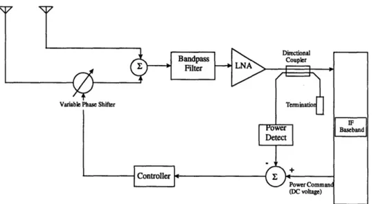
So far in this report, we have seen a few of the problems faced by the designer of a modem microwave receiver. Chief among those problems is the phenomenon of fading; it has been stated that spatial diversity can be exploited to counteract this. The need for a variable attenuator has been firmly established. The proposed system is an integration of these two concepts. A block diagram is shown in figure 1-6. The idea is to build an automatic gain control in the RF front end of the receiver. A desired power input is given to the system in the form of a DC voltage, and the controller adjusts the phase relationship between the two antennas until that power level is achieved. If the desired power is greater than the total power available, the controller should adjust the phase until the received power is maximized.
Figure 1-6: The proposed system
In addition to providing the benefits of a continuously variable attenuator and of antenna diversity, this system also has a few other features. Among them:
* The antenna diversity does not come at the price of additional RF parts, such as LNA's. Most multiple-antenna, systems do the phase manipulation in baseband processing. This approach requires that each antenna have its own LNA, bandpass filter, and mixer. LNA's and mixers in particular can be expensive RF components.
* It is completely modular, in that it could be used as the front end of any receiver. This would not be the case, say, if the controller itself was one of many processes running on the baseband DSP chip. The system would then be inextricably linked to the receiver it was designed for. In the current form, however, it would be marketable as a stand-alone "smart"
antenna.
Chapter 1 References
[1] A. Santamaria, F.J. Lopez-Hernandez, Wireless LAN Systems. Norwood, MA: Artech House, 1994.
[2] H. A. Haus, et al., "Representation of Noise in Linear Twoports," Proc. IRE., vol. 48, pp. 69-74, Jan. 1960.
[3] D. Pozar, Microwave Engineering. Addison-Wesley, 1990.
[4] T. A. Denidni and G. Y. Delisle, "A Nonlinear Algorithm for Output Power Maximization of an Indoor Adaptive Phased Array," IEEE Trans. Electromagnetic Compatibility, vol. 37, pp. 201-209, May 1995.
[5] W. C. Y. Lee, Mobile Communications Design Fundamentals. John Wiley & Sons, Inc., 1993.
[6] W. C. Jakes, "Multipath Interference," Ch. 1 in Microwave Mobile Communications, W. C. Jakes, editor. Piscataway, NJ: IEEE Press, 1974.
[7] J. Liang, "Radio Propagation in Cellular Environments," presentation at Bell Laboratories, Lucent Technologies, August 8, 1996.
[8] K. Kagoshima, W. C. Y. Lee, K. Fujimoto, K. Hirasawa, and T. Taga, "Essential Techniques in Mobile Antenna Systems Design," Ch. 2 in Mobile Antenna Systems
Handbook, K. Fujimoto, J. R. James, editors. Norwood, MA: Artech House, 1994.
[9] Reference Data for Engineers: Radio, Electronics, Computer, & Communications. Carmel, Indiana: SAMS, Prentice Hall Computer Publishing, 1993.
[10] J. Liang, "Space-Time Diversity Combining and Equalization in TDMA(GSM) Networks," presentation at Bell laboratories, Lucent Technologies, September 10, 1996.
[11] J. H. Winters, J. Salz, R. D. Gitlin, "The Impact of Antenna Diversity on the Capacity of Wireless Communications Systems," IEEE Trans. Commun., vol. 42, pp. 1740-1751, Feb./March/April 1994.
[12] T. Ohgane, T. Shimura, N. Matsuzawa, H. Sasaoka, "An Implementation of a CMA Adaptive Array for High Speed GMSK Transmission in Mobile Communications," IEEE
Trans. Vehicular Technology, vol. 42, pp. 282-288, Aug. 1993.
[13] W. Gabriel, "Adaptive Arrays---An Introduction," Proc. of the IEEE, vol. 64, pp. 239-272, Feb. 1976.
[14] S. Y. Liao, Microwave Circuit Analysis and Amplifier Design. Englewood Cliffs, NJ: Prentice-Hall, Inc., 1987.
[15] P. Vizmuller, RF Design Guide: Systems, Circuits, and Equations. Norwood, MA: Artech House, 1995.
[16] S. O. Rice, "Mathematical Analysis of Random Noise," Bell System Tech. J., vol. 23, pp. 282-332, July 1944; vol. 24, pp. 44-156, Jan. 1945; "Statistical Properties of a Sine Wave Plus Random Noise," Bell
Chapter 2: The Theory Behind the Method
The method that the proposed system employs is commonly referred to as "equal gain combining." As the name implies, the signals received from the two antenna elements are equally weighted, with only their phase relationship subject to the demands of the controller. It will be shown in this chapter that this represents a tradeoff between two other combining methods, achieving an effective compromise between the simplicity of one and the superior performance of the other. In addition, the algorithm implemented by the controller is introduced. The details of the controller itself, together with an analysis of its behavior, are the substance of
Chapter 3.
Methods of Spatial Combining
The basic problem that deep fades introduce is one of information loss: the signal vanishes into the noise floor, while the bit-error rate, to extend the analogy, goes through the roof. The ideal would be to transmit and receive a signal that does not fade; this is an impossibility in most modem systems. We can improve things, however, by making several copies of the signal available to the receiver, where each copy fades independently of the rest. A
complete information loss then requires a deep, simultaneous fade on all of the received copies, and we find that the laws of probability work on our behalf. This illustrates the simple concept behind diversity techniques, as they are called: the likelihood of such an event clearly decreases with increasing degree of diversity. We will show that significant gains can be made in going from a single copy to even two-fold signal diversity.
Convinced that diversity is a good idea, we still find ourselves far removed from an actual solution. How, for instance, does one intelligently combine the multiple copies to yield the greatest benefit? Or, more fundamentally, how do you get multiple copies in the first place? The most obvious answer to the second question has already been introduced, which is to employ multiple antennas at the receiver site. By spacing them at least a half wavelength apart, one can ensure that the fading behavior of each signal will exhibit small correlation with that of the others. Other existing methods include: (1) transmitting signals sufficiently separated in time; (2) transmitting copies on orthogonal polarizations; (3) the use of directive antennas (transmitting or receiving) that point in widely different directions; (4) transmitting the same signals on sufficiently different carrier frequencies [1]. The use of multiple receiving antennas will be focused on here, as it is the most common method and the method chosen for this thesis project. Within this context we will examine the more pressing question of how to combine the multiple copies in a meaningful way.
Selection Diversity
One rather intuitive approach to the combining problem is, strictly speaking, not to combine. In a selection diversity scheme, a continuous comparison (on the basis of signal-to-noise ratio (SNR)) is made between the diversity branches. The SNR is sometimes difficult to measure in practice; often the branch with the largest signal plus noise (S + N) is assumed to have the greatest signal content. The branch with the highest SNR is then connected to the rest of the receiver, and this remains the state of affairs until a different branch exhibits the highest SNR. This approach offers the clear advantage of simplicity, while yielding a substantial benefit in terms of reducing the bit-error rate. It is instructive to examine the nature of this benefit mathematically.
P(r) = r e-r /2b, r _ 0 (1-16) b
= 0 O.W.
For the purposes of a fading discussion, it is useful to consider the probability that the signal strength will fall below a certain value. We will denote the cumulative distribution function as P{r 5 R}, which is the probability that the amplitude, r, is less than or equal to R.
P{r, < R} = 0 if R<O
= 2bdr -rie-r O.W. (2-1)
We are fortunate in that the antiderivative (2-1) is easily done by inspection:
R r-!eri22bdr =[-e-2I2b R
b 1 O
= 1- e-R22b (2-2)
Our real interest, of course, is in the signal-to-noise ratio. If we assume that the noise power is constant, and that that power is independent of the branch, a recasting of the equation into the appropriate form is not difficult. The mean signal power in a branch, averaged over one cycle, is
r 2 /2, and let the mean noise power in a single branch be N. The probability that the local mean SNR is less than some value ys is equal to the probability that
2N
j
< 7 (2-3)ri2 < 2Nys (2-4)
rI < 2, ,2Ny (2-5)
where that last step is possible because all quantities concerned are positive. The probability that the SNR will be less than some value y, can now be expressed as
P{iy, y,} = 1- e-N7'Ib (2-6) Finally, we recognize b/N as the global mean signal power to mean noise ratio, and rewrite (2-6)
as
(2-7)
P{y, <y, } = 1- e-r,/r
where F is b/N. Now it can be seen why this method of selection diversity is successful. If we assume that the switching mechanism is instantaneous and free of noise, the probability that the receiver will be fed a signal with SNR less than y, becomes
P{Yi "'M s} = (1-e-,/r )M,
(2-8)
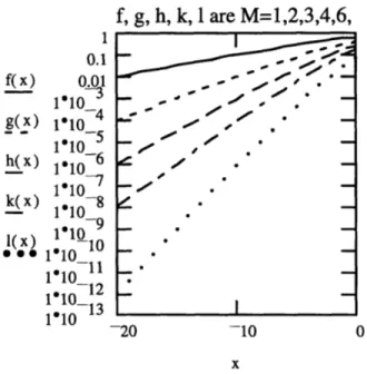
where M is the number of receiving elements (or, more generally, the degree of diversity). Since the quantity being raised to the power M is always less than one, it is clear that we do better as the number of antennas increases. As to seeing how much better, it is instructive to look at a graph. f(x) g(x)h( x)
k( x) *(x) 0oo 1 0.1 0.01 1010 -4 1010 1010 -5 1010 1 10 1 1610 -8 110 1"10 1 110 12 11013 f, g, h, k, 1 are M=1,2,3,4,6, -20 -10 xFigure 2-1: Probability that a fade of depth x will occur for various values of M
In this graph, x is yl/F, in decibels, and f, g, h, k, and 1 are the cumulative distribution functions for various values of M. If we compare probability statistics at the "likelihood of a 20dB fade"
gh
-S00
mark, we see that each new antenna element gets us about two orders of magnitude in improved performance.
It is also, for purposes of a later comparison, useful to look at the mean SNR. The end result of this calculation is [1]:
(,)= F_-.
(2-9)
k=1 k
There are a couple of important things to take away from the preceding exercise. First and foremost, it confirms our intuition that, from an information recovery standpoint, diversity is a good thing. We took for an example the most naive form of combining, and saw dramatic increases in deep-fade performance. Second, it should be noted that it is probably not in the engineer's best interest to push antenna diversity to the extreme, particularly if the design is for a hand-held unit. You can see from the graph that even the addition of a single element results in a significant improvement, with the extra advantage of allowing a relatively simple switching scheme.
Maximal Ratio Combining [1]
Selection diversity has thus far been discussed as an intuitive, first iteration, non-optimized way of beating the fading problem. This characterization, while accurate, should not be taken to mean that it is never used: in many mobile units, where cost is of extreme importance, this method finds ready applicability. Still, we have to believe that, cost aside, there is a way to achieve even higher performance. One way, referred to as maximal ratio combining, is presented here.
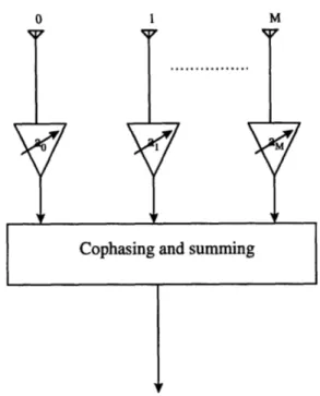
In a maximal ratio combining system, the various receiving branches are cophased, weighted in some optimal manner, and summed. A general diagram for such a scheme is shown in figure 2-2.
0 1 M
Figure 2-2: A maximal ratio combining system
It turns out that the optimal weighting (for any linear combiner) is to choose each ai to be proportional to the ratio of signal amplitude to noise power in that branch. That is,
a. oc
-.
(2-10)The SNR out of the combiner winds up being the sum of the branch SNR's. As long as none of the branches has an SNR of less than one, we are guaranteed an improvement with each
additional branch. The mean SNR of the combined signal is simply expressed:
M M
,=
yr= F = Mr. (2-11)
i=1 i=1
Equal Gain Combining [1]
Equal gain combining is something of a compromise between the two methods previously shown. In this method of fading reduction, signals from all of the antenna elements receive the same weight, and are cophased. The mean SNR for this type of combining is
It has the benefit of being simpler to implement than maximal ratio combining, while offering performance that is superior to that of a selection diversity scheme.
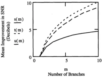
We are now in a position to compare the three approaches. This is best shown graphically, although it is clear from the equations which methods offer the best performance per added branch of diversity. With maximal ratio combining, the mean SNR increases linearly with the number of receiving elements. This is also true in the case of equal gain combining, although the slope of that line is smaller. Selection diversity is a clear loser in this contest, particularly in systems which employ a high degree of diversity.
10
z
S s(m) St(m) 5 Su(m) ou 0 5 10 m Number of BranchesFigure 2-3: A comparison of three combining methods
In Figure 2-3, s corresponds to selection diversity, t to maximal ratio combining, and u to equal gain combining. We see that a switch from selection diversity to equal gain combining yields an impressive boost in performance. The same cannot be said for a similar switch from equal gain to maximal ratio combining.
We have now established a context within which to view the proposed system. A reexamination of figure 1-6 reveals that we are implementing a type of equal gain combining. But there is an important difference: in implementing an automatic gain control, we have departed from the typical scheme in that the two signals will not always be cophased. For purposes of a fading discussion we must consider two cases: (1) the desired power is
-
-I,
r~o
unattainable in the given environment; (2) a phase relationship between the two signals exists such that, if obtained, the desired power can be met exactly.
The first case establishes an important specification on the design of the controller. If the situation arises in which the desired power is unattainable, the controller must do its best. That is to say, it must maximize the received power if the command level is too high, and it must minimize the received power if the command level is too low. If it is desirable to mimic the behavior of typical equal gain combining schemes, one need only to set the command level to an unrealistically high level. The reader may find the idea of minimizing the received power curious; in theory, complete cancellation is possible if the gains are equal. Two things, however, render this idea useless in practice. First, based on what we know about fading, we can be almost assured that the signals at their respective antenna elements are not of exactly the same amplitude. Second, even if they were of the same amplitude, complete cancellation would necessitate the use of a perfectly lossless phase shifter. Once again, we run into an idea that is useful only as a theoretical abstraction.
The second case is the best possible if our sole objective is to have a combined received signal that does not fade. However, it is important to note that the question of which case is pertinent has, in general, a very time dependent answer. This is particularly true if the fading envelope of the two received signals exhibits unexpectedly correlated behavior: a deep, simultaneous plunge in received power at both elements may cause an ordinarily reasonable power command to be unattainable.
At this point, the reader should recognize the RF AGC as the system-level tradeoff that it is. We are not maximizing the received SNR, which is what we should do from an information recovery standpoint. Rather, we are deciding on an SNR that is "good enough," and making more effective use of our LNA. In so doing, we are introducing a kind of intelligent behavior that is new to the field of "smart" antennas.
The Problem of Designing a Controller
The focus of this section will be on some of the difficulties that the controller in figure 1-6 must overcome. Also, the basic algorithm is introduced.
Specifications for the Controller
The design of the feedback controller is complicated by the fact that the sign of the loop transmission is uncertain. This problem owes its existence to the nonlinear, time-varying transfer function between a phase change and the resultant change in detected power. This is best shown mathematically; consider the sum of two equal-frequency sinusoids that differ only in phase. If we examine the magnitude squared,
IAe'"ej j + Aej"e" 2 = 2A2 (1+ cos( - )) (2-13)
we can see the exact nature of the non-linearity. Denoting the phase difference as a and differentiating, we can linearize this function and look at its behavior for small fluctuations in phase about a set operating point:
d
d-[2A2(1+ cosa)] = -2A2 sina. (2-14)
da
If the operating point is beyond our control, as it is in this case, the incremental relationship between a phase change and a change in received power cannot even be ascertained to within a minus sign. In a mobile environment, the problem is exacerbated by the random time-varying nature of this relationship: the phase difference between the two received signals (before they are processed) is what determines the operating point, and this changes as the receiver moves.
All that is clear at this point is that a classic, linear feedback loop is not an option. However, we have something to learn from their basic operation. The key to feedback controllers is that they seek to minimize the absolute value of the error. The direction that the input of the plant needs to be "pulled" to correct for, say, an output that is too small, is known a
priori by the system designer; s/he is thus able to ensure that the sign of the loop transmission is correct.
As it happens, our problem has an additional difficulty: if by guessing we happen to get the sign of the loop transmission right initially, it is probable that this would be a temporary state of affairs. The controller must be able to rapidly adapt to this changing sign.
The fading behavior also gives us constraints (or, at least, goals) to shoot for as far as loop speed is concerned. It has been stated that carrier envelope is bandlimited to twice the maximum Doppler shift, which scales linearly with vehicle speed and as the inverse of the carrier wavelength. It is currently common for mobile systems to use carriers that are close to 1 GHz, and a reasonable worst-case speed would be sixty miles per hour; the spectral content of the fading envelope thus has an upper bound of 180 Hz. Prudence demands that this not be the outer limits of the controller's ability; we chose a safety margin of a factor of ten. Ideally, then, the controller should be able to handle the fading of a 10 GHz carrier when the receiver is moving at 60 mph (an envelope bandlimited to about 2 kHz).
The Basic Algorithm
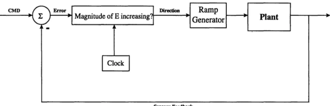
The basic behavior of the controller is based on an algorithm that was introduced and analyzed by Trybus and Hamza [2, 3]. It was intended for use in extremum controllers, whose purpose was to operate an industrial process at an extreme value of the process output; it has since been applied to antenna arrays by Denidni and Delisle [4] to maximize received power. In this implementation the controller moves its output in a given direction for a fixed amount of time, continuously monitoring the error. If the magnitude of the error is increasing, the controller changes direction for the next time step. Otherwise, it keeps moving in the same direction. The system will, in the steady state, fluctuate about the desired value. A simplified diagram depicting this behavior is shown in figure 2-4.
Sensory Feedback
Figure 2-4: Block diagram of controller
Simple though it is, it can be seen that it satisfies, or has the potential to satisfy, all of the specifications that so concerned us in the last section. We have no reason to suppose that the loop bandwidth has some prohibitive limit. And it is clear that, should the incremental gain of the plant suddenly switch sign, the controller would adapt within one system clock cycle. We have, it would appear, every reason to be optimistic.
Design Issues
Of course, implementation rarely fails to bring to light a myriad of "subtle" difficulties. Some of these difficulties will be briefly described in the next few paragraphs.
To begin with, there are performance tradeoffs that simply come with the algorithm. It turns out that the tracking ability of the controller is most closely related to the rate of change of its output (the input to the plant) during a time step. A short thought experiment bears this out: if we imagine a ramp input whose slope exceeds that of the controller output (or, more properly, that of the controller output multiplied by the incremental gain of the plant), the error will increase regardless of the direction chosen. The result will be that it will oscillate, mired in indecision, until the slope becomes trackable. The tradeoff is that for a fixed clock speed, the DC steady-state error increases in proportion to the slope during a step. The best solution is to remove the constraint that the clock rate be fixed. Given the finite bandwidth character of any imaginable implementation, however, we must accept that at some point this option will not be available to us.
There is another option, which is to dynamically vary the slope of the controller's output as the system deems appropriate. In that way, the aforementioned tradeoff can be beaten to a certain extent. It will be seen in the next chapter how this behavior was added, and the benefit that it produced.
Additional difficulties are introduced when you begin to talk about the real, physical plants that this system is being designed to control. By far the most serious concern is that of the plant bandwidth. We have advanced a 2 KHz bandwidth as a reasonable goal for the loop speed. If we were dealing with a linear feedback loop, this would require the plant to have around 2 KHz of bandwidth (perhaps less, if well compensated). It can be seen in our system, however, that acceptable following behavior would demand a clock rate that is an order of magnitude, if not two, greater than the maximum tracking bandwidth. If the controller is going to know how well it is doing in time to make a good decision on the step direction, the bandwidth of the plant must be correspondingly high. That is, to say the least, of non-trivial consequence. One is forced to accept that this algorithm is best suited to the application its creators had in mind: operating a slow industrial process at an extreme of the process output. Asking it to do rapid tracking (or, equivalently, disturbance rejection) is pushing it in ways that it might not willingly
go.
Dynamics of the plant notwithstanding, its linearity is of some concern. A highly nonlinear transfer function between the input and output of the plant will introduce distortion into the otherwise linear step the controller is trying to take. Worse is the prospect of said transfer function having more than one extremum: one can easily imagine a scenario in which the controller gets itself "trapped."
A full appreciation of these issues was gradually acquired through the process of building and debugging the complete prototype. We now turn our attention to the first major building block of that prototype: the controller itself.
Chapter 2 References
[1] W. C. Jakes, Y.S. Yeh, M. J. Gans, D. O Reudink, "Fundamentals of Diversity Systems," Ch. 5 in Microwave Mobile Communications, W. C. Jakes, editor. Piscataway, NJ: IEEE Press, 1974.
[2] L. A. Trybus, "Extremum Controller Design," IEEE Trans. Automatic Control, vol. AC-21,
pp. 388-391, June 1976.
[3] M. H. Hamza, "Extremum Control of Continuous Systems," IEEE Trans. Automatic
Control, vol. AC11, pp. 182-189, Apr. 1966.
[4] T. A. Denidni and G. Y. Delisle, "A Nonlinear Algorithm for Output Power Maximization of an Indoor Adaptive Phased Array," IEEE Trans. Electromagnetic Compatibility, vol. 37, pp. 201-209, May 1995.
Chapter 3: Design and Analysis of the Controller
In the initial stages of this project, a great deal of time was spent on the details of the basic, non-adaptive behavior of the controller. A subsequent literature search established the age of this "new" idea as greater than twenty years. Still, the design of the prototype proved to be a worthy technical challenge, and the adaptive behavior added as an optimization seems to be a true innovation. The operation of the controller was partially described in Chapter 2. The purpose of this chapter is to examine it in its circuit implementation.
Overview of the Circuit
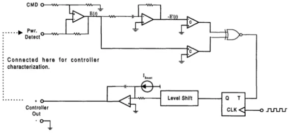
CMD ... Pwr. Detec Connected characteriza Contr Ou J1JJ-Lr
Figure 3-1: Your basic controller
It can be seen in figure 3-1 how a "step" is mechanized. The voltage input to the op-amp integrator can assume one of two values (one positive, the other of the same magnitude but negative), which is then integrated to produce a ramp for the duration of the clock cycle. The current source, Iboost, is an optimization that allows the slope of the ramp to be dynamically varied. The error is computed by a simple difference amplifier, and by examining the sign of the error and of its first derivative it is determined whether the magnitude is growing or shrinking (e.g., if the error and its first derivative have the same sign, the magnitude of the error is growing).
Figure 3-1 also shows that, for the initial characterization effort, the controller output was connected directly to the "power detect" input. In so doing, the circuit is made to mimic a unity gain feedback amplifier. By driving the "CMD" input with a sine wave and observing the output, the bandwidth of the loop2 could be determined. Of course, this is not quite how the loop will be used in a real system. The "CMD" input will be tied to a DC voltage, and the circuit's responsibility will be to null out the what would otherwise be disturbances in the received power
2 The word 'bandwidth' is used somewhat loosely here. It will turn out that the sinusoidal response and
the step response are not mathematically coupled in the same way that they are for a linear system. Additionally, the amplitude of a signal is as important as its spectral content in determining whether the system can track it. One could argue that the term 'bandwidth' has lost some of its utility. We will continue to use it here, with the understanding that perhaps 'speed' is closer to what we mean.
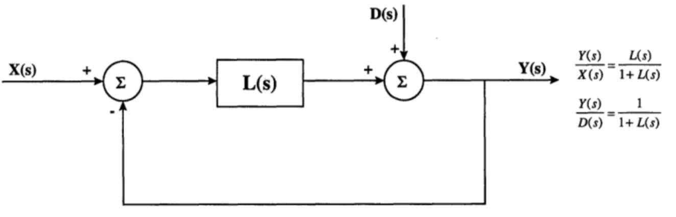
level. It turns out that a feedback loop's ability to reject a disturbance is completely equivalent to its ability to follow a command. Figure 3-2 shows why.
Y(s) L(s)
X(s) 1+ L(s) Y(s) 1
D(s) 1+ L(s)
Figure 3-2: Comparison of command and disturbance transfer functions
If we subtract the disturbance transfer function from unity (which gives us a useful figure of merit for disturbance rejection), we arrive at the same expression relating the command signal to the output. Granted, the diagram depicts a linear feedback loop, which is not what this system is. But the principle still holds, as one can readily convince oneself. For the skeptic, an actual experiment was done that bore this out.
Referring again to figure 3-1, it can be seen that the differentiation was carried out by an actual analog differentiator. This in contrast to, say, using a sample-and-hold circuit with a difference amplifier. Initially it was thought that the latter approach would be safer, given the analog differentiator's fearsome reputation for noise susceptibility. It turned out, however, that the cost of the op-amp was smaller than that of the S/H by about two orders of magnitude; we were thereby persuaded that the noise problems could be overcome.
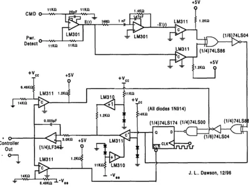
Design of the Non-Adaptive Circuit
Figure 3-3 depicts an early prototype of the controller, before its performance had been optimized by the addition of the Iboost current source.