Development of chipscale chalcogenide
glass based infrared chemical sensors
The MIT Faculty has made this article openly available.
Please share
how this access benefits you. Your story matters.
Citation
Juejun Hu, J. David Musgraves, Nathan Carlie, Bogdan Zdyrko, Igor
Luzinov, Anu Agarwal, Kathleen Richardson and Lionel Kimerling,
"Development of chipscale chalcogenide glass based infrared
chemical sensors", in Quantum Sensing and Nanophotonic Devices
VIII, (Proc. of SPIE 7945, 79452C (2011). © 2011 SPIE.
As Published
http://dx.doi.org/10.1117/12.871399
Publisher
Society of Photo-optical Instrumentation Engineers
Version
Final published version
Citable link
http://hdl.handle.net/1721.1/71812
Terms of Use
Article is made available in accordance with the publisher's
policy and may be subject to US copyright law. Please refer to the
publisher's site for terms of use.
Development of chipscale chalcogenide glass based infrared chemical
sensors
Juejun Hu*
a, J. David Musgraves
b, Nathan Carlie
b, Bogdan Zdyrko
b, Igor Luzinov
b, Anu Agarwal
c,
Kathleen Richardson
b, and Lionel Kimerling
ca
Department of Materials Science & Engineering, University of Delaware, Newark, DE 19716, USA
bSchool of Materials Science & Engineering, COMSET, Clemson University, Clemson, SC 29634,
USA
c
Microphotonics Center, Massachusetts Institute of Technology, Cambridge, MA 02139, USA
ABSTRACT
In this paper, we review the design, processing, and characterization of novel planar infrared chemical sensors. Chalcogenide glasses are identified as the material of choice for sensing given their wide infrared transparency as well as almost unlimited capacity for composition alloying and property tailoring. Three generations of on-chip spectroscopic chemical sensor devices we have developed: waveguide evanescent sensors, micro-disk cavity-enhanced sensors and micro-cavity photothermal sensors are discussed.
Keywords: Chalcogenide glasses, sensors, resonators, integrated optical devices, spectroscopy
1. INTRODUCTION
Recent advances in nano-fabrication technology have enabled a paradigm shift in the field of chemical and biological detection. Miniaturized sensing devices can now be created that outperform and possibly replace their conventional bulky counterparts. These devices build on the knowledge base and technologies developed in photonics, micro-fluidics, and micro-electronics and have given rise to sensing/characterization platforms commonly referred to as a “sensor-on-a-chip” or “lab-on-a-chip”1. The competitive advantages of such miniaturized sensing devices are three-fold.
Firstly, the Moore’s law paradigm driving the rapid strides of micro-electronics can be applied to revolutionize bio-/chemical detection, leveraging mature silicon CMOS manufacturing technology to achieve high volume production and thus very low cost, as well as scalable performance improvement2. Secondly, a small device footprint opens up avenues
of new device and system applications such as remote sensor network deployment. These networks for example are impossible (cost prohibitive) with a conventional, large footprint design. Lastly, integration of different functional components onto a planar platform enables multi-modal detection and significantly enhanced intelligence capabilities. Chalcogenide glasses (ChGs) are well-known for their high infrared transparency and amenability to fabrication in fiber and thin film forms which makes them attractive candidates for infrared optical chemical sensors3-7. Recent efforts in our
group have focused on the development of a novel, integrated sensor system with enhanced sensitivity and specificity suitable for use in advanced chemical-biological detection applications, based on novel chalcogenide glass materials8-12.
These efforts have resulted in the development of Si-CMOS compatible processing procedures and demonstration of viability of manufacturing uniformity to large areas (> 6” diameter wafers)13. Such progress provides a means to
evaluate scalability and economics in fabricating and integrating optical structures and devices for use in chip-based chemical and/or biological sensors. The novelty of the resulting sensor design is three-fold:
1) novel high refractive index chalcogenide glass materials suitable for multi-spectral chemical sensing have been developed which allow extension of the operating wavelength range for devices from the UV to visible to far infrared. ChGs enable use of a low temperature process to fabricate an ultra-high-Q optical resonant cavity with an atomically smooth surface14, leading to strong photon-molecule interactions and high detection sensitivity;
2) compared to fiber-based counterparts, planar ChG-based resonator devices are more mechanically robust and amenable to lower cost, larger-scale integration with other on-chip photonic and electronic devices, enabling a full spectrum of optical signal read-out and processing functions;
*[email protected]; phone 1 302 831-6878; fax 1 302 831-4545. Invited Paper
Quantum Sensing and Nanophotonic Devices VIII, edited by Manijeh Razeghi, Rengarajan Sudharsanan, Gail J. Brown, Proc. of SPIE Vol. 7945, 79452C · © 2011 SPIE · CCC code: 0277-786X/11/$18 · doi: 10.1117/12.871399
3) the sensor device fabrication strategies developed and optimized in this effort employs CMOS-compatible processing technology suitable for mass production and further scalable performance improvement. Such scalability reduces per sensor costs allowing multi-sensor arrays tailorable to single or multi-species detection to be deployed for large sampling area evaluation. No other current technology offers such possibility.
The sensing mechanism of chalcogenide glass optical chemical sensors are based on optical absorption spectroscopy, where the device detects the absorption of target molecules. The performance matrix of optical chemical sensors consists of two key parameters: specificity and sensitivity/accuracy. Specificity of our technique is provided by fitting the measured spectra with the molecular absorption characteristic fingerprints. Notably, such an operation principle is similar to that of conventional Fourier-Transform InfraRed (FTIR) spectroscopy, and therefore the data fitting algorithms and analytical methods such as Principle Component Analysis (PCA) traditionally employed for FTIR data analysis may also be applied to further improve the detection specificity. Further, we have demonstrated significant molecule identification capability improvement by functionalizing the sensor surfaces with polymer coatings engineered to provide selective enrichment of target molecular species. Applications of such polymer coatings for improving sensor specificity have been detailed elsewhere and is not the focus of this paper15.
Sensitivity/accuracy refers to the detection limit of the sensor and the error associated with concentration readings in quantitative measurements. In the past years, we have focused on improving the detection sensitivity and accuracy by enhancing the light-molecule interactions using novel device architectures. In this paper, we will review the three generations of chalcogenide glass-based on-chip spectroscopic sensors we have developed for chemical detection applications.
2. CHALCOGENIDE DEVICE PROCESSING AND TESTING
Ge23Sb7S70 glass has been selected for our sensor device fabrication given its good chemical and structural stability. Bulk
Ge23Sb7S70 glass was prepared from high purity elements using a traditional chalcogenide melt-quenching technique16.
Details of the bulk sample preparation process may be found elsewhere18. The high-quality glass bulk was then thermally
deposited onto 6” Si wafers already coated with a 3 μm thermal oxide layer (Silicon Quest International Inc.) in a custom-designed thermal evaporator (112 Evaporator-Sputter Station from PVD Systems Inc.). The film was deposited at a base pressure of 2×10⁻⁷ Torr using a Tantalum baffled source, and the deposition rate was stabilized at 18 Ǻ/s. The
final thickness of the films used for device fabrication is fixed at 450 nm. The Si substrate was mounted on a thermostat stage and was thus maintained at room temperature throughout the deposition process. Waveguide and resonator devices were subsequetly patterned by lift-off, and the whole patterning process has been carried out on a 500 nm CMOS line13.
The CMOS-compatibility allows this process to be scaled up for mass production. PDMS (Sylgard 184 Silicone Elastomer, Dow Corning Inc.) microfluidic channels with a width of 100 μm and a height of 30 μm are fabricated via replica molding. After oxygen plasma treatment, the channels are irreversibly bonded onto the chips on which the microdisks are patterned. Liquid inlet and outlet access holes are punched prior to bonding, and PTFE (polytetrafluoroethene) tubing is attached into the access holes to complete the microfluidic chip fabrication.
Transmission spectra of the fabricated devices are measured on a Newport AutoAlign workstation in combination with a LUNA tunable laser (optical vector analyzer, LUNA Technologies, Inc.). Lens-tip fibers are used to couple light from the laser into and out of the devices. Reproducible coupling is achieved via an automatic alignment system with a spatial resolution of 50 nm. During testing, analyte solution was injected into the channels via a syringe pump. The sample is mounted on a thermostat stage and kept at 25 ˚C for all measurements.
3. WAVEGUIDE EVANESCENT WAVE SENSOR
The operating principles of a Waveguide Evanescent Wave Sensor (WEWS) is similar to that of a Fiber Evanescent Wave Sensor (FEWS)4. At selected wavelengths corresponding to the characteristic absorption bands of the target
molecules, light propagating in the waveguide is attenuated due to the interactions of evanescent waves with the molecules. Advantages of WEWS devices include simple device fabrication and straightforward data interpretation. However, according to the Lambert-Beer law, high sensitivity is only possible in WEWS when long waveguide length is used. Such a requirement leads to the trade-off between sensitivity and device footprint. Serpentine or spiral waveguide structures may be used to reduce footprint requirements but considerable on-chip real estate is still necessary to attain high detection sensitivity and accuracy17.
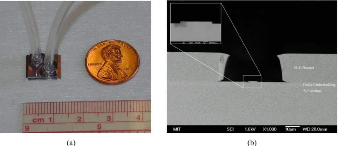
In our WEWS experiment, fabricated Ge23Sb7S70 waveguide wafer was cleaved into 12 mm × 8 mm dies prior to testing.
Figure 1(a) shows a photo of the assembled microfluidic chip with fluid inlet and outlet tubing. SEM cross-sectional images (taken on a JEOL 6320FV field-emission high-resolution SEM) of the waveguides in Fig. 1(b) exhibited a vertical sidewall profile and excellent feature size fidelity. Ge23Sb7S70 waveguide transmission loss was measured using
paper-clip waveguide patterns defined on the same wafer as the sensor devices to be (2.3 ± 0.3) dB/cm at 1550 nm wavelength.
(a) (b)
Figure 1. (a) Photo of the assembled microfluidic chip with fluid inlet and outlet tubing; the microfluidic channels and Ge23Sb7S70 waveguides are too small to resolve in the image.
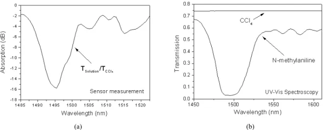
Sensor performance was tested by monitoring the optical output while injecting a solution of N-methylaniline mixed with a solution of carbon tetrachloride into the microfluidic channel. The N-H bond in N-methylaniline is known to exhibit an absorption peak near 1500 nm18, which was used as the characteristic fingerprint for chemical identification in
our test. The absorption (in dB), αL, induced by N-methylaniline in our microfluidic channel was calculated by taking the ratio of light intensity transmitted through a microfluidic channel filled with pure carbon tetrachloride (Isolvent) and
through a channel filled with N-methylaniline solution in carbon tetrachloride (Ianalyte) (0.33, volumeric concentration),
i.e. analyte solvent I I L=10log10 α (1) with L the length of the waveguide immersed in analyte solution (cm). The same waveguide was used throughout the
experiment to eliminate any uniformity issue associated with waveguide intrinsic loss. The resultant absorption spectrum shown in Fig. 2(a) exhibits a well-defined absorption peak at 1496 nm, which is in excellent agreement with a traditional absorption measurement carried out on a Cary 5E UV-Vis-NIR dual-beam spectrophotometer as seen in Fig. 2(b). As seen in Fig. 2(b), since carbon tetrachloride has no absorption band and is transparent in the investigated range, this spectral peak is unambiguously assigned to N-H bond vibrational absorption.
The peak absorption in dB at 1496nm was measured for different concentrations of N-methylaniline solution in carbon tetrachloride and the result is shown in Figure 3. The excellent linear fit suggests that the sensor exhibits linear response when varying analyte concentrations. Fluctuations of input laser power, which primarily stem from the spatial shift of input/output fibers in our case, have been the dominant noise source in our measurement. The noise induced by the power fluctuations has been estimated to be ~ 5%, which corresponds to 0.21dB. The minimum detectable concentration of the sensor to N-methylaniline can thus be calculated to be 0.7 vol. % of N-methylaniline in carbon tetrachloride. The relatively low sensitivity measured experimentally in the case of N-methylaniline is due to its low absorption coefficient at 1496 nm. Using mid-infrared probing wavelength, which is highly absorbed in the medium, could significantly enhance sensor performance. Further improvement of the detect limit requires new device designs as we will detail in the next sections.
(a) (b)
Fig. 2. (a) Absorption spectrum showing the N-H bond absorption at 1496 nm wavelength in N-methylaniline measured using our integrated evanescent sensor. The absorption is defined by taking the ratio of light transmission in the case of a microfluidic channel filled with pure carbon tetrachloride against the case when the channel is filled with N-methylaniline solution in carbon tetrachloride (0.33, volumetric concentration). (b) Transmission spectra of pure N-methylaniline and carbon tetrachloride (CCl4) measured using
traditional UV-Vis spectroscopy. The absorption spectrum of N-methylaniline shows the same N-H absorption peak near 1496 nm while carbon tetrachloride is transparent in the wavelength range of interest.
Fig. 3. Peak absorption of N-methylaniline solution in carbon tetrachloride at 1496 nm wavelength measured using the waveguide evanescent sensor as a function of N-methylaniline volume concentration, indicating good linearity of the sensor response.
4. MICRO-DISK CAVITY-ENHANCED SENSOR
The trade-off between detection sensitivity/accuracy and device footprint can be overcome by using a resonant cavity (optical resonator), which offers resonantly-enhanced, long optical path length while still maintaining a small physical device size19-21. We have demonstrated micro-disk resonators in chalcogenide glasses with cavity Q-factors up to 5 × 10⁵
and finesse exceeding 2,000, corresponding to over three orders of magnitude resonant enhancement of optical path length11. We use the optofluidic Ge
23Sb7S70 resonator device to measure the well-defined absorption peak of
N-methylaniline near 1500 nm. A top view micrograph of the fabricated microfluidic channel overlaid with a linear array of Ge23Sb7S70 microdisks is shown in Fig. 3(a), and Figure 3(b) is a photograph of the optofluidic resonator device under
testing. Quality factors (Q) of the resonators under testing is within the range of 130,000 (± 15%) in pure CCl4, which
corresponds to a linear waveguide loss of ~ 1.5 dB/cm. During the cavity-enhanced spectroscopic test, N-methylaniline solutions in carbon tetrachloride of varying concentrations are injected into the channels using a syringe pump and the optical transmission spectra of the resonators are monitored in situ.
(a) (b)
Figure 4. (a) Top view micrograph of a PDMS microfluidic channel overlaid with a linear array of 20 μm radius Ge23Sb7S70 microdisks; (b) photograph of an optofluidic chip under testing.
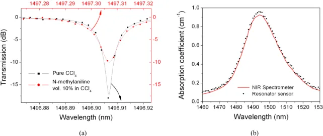
Figure 5(a) shows the transmission spectra around a resonant peak, both before and after injection of 10% vol. N-methylaniline solution in CCl4 into the microfluidic channel. The resonator works in an under-coupling regime; therefore
the additional optical loss due to N-methylaniline absorption results in a decrease of the extinction ratio along with a broadening of the resonant peak. The optical absorption of N-methylaniline solution can be extracted based on the resonant peak extinction ratio change10. Figure 5(b) plots the optical absorption spectra of 10 vol. % N-methylaniline
solutions measured using Ge23Sb7S70 resonator sensor and an NIR spectrometer, showing excellent agreement between
the two techniques. Note that each point on the spectra measured by the resonator sensor corresponds to a resonant peak, and the spacing between the points (spectral resolution) is determined by the resonator free spectral range.
(a) (b)
Figure 5. (a) Microdisk transmission spectra around a resonant peak before and after N-methylaniline solution injection: the dots are experimentally measured data points and the lines are theoretical fitting results based on the generalized coupling matrix formalism; the extinction ratio change and resonant peak broadening are due to the optical absorption of N-methylaniline near 1500 nm. Note that the resonant wavelength red shifts due to the refractive index difference between pure CCl4 and N-methylaniline solution; (b) optical absorption spectra of 10
vol. % N-methylaniline solution measured using Ge23Sb7S70 resonator sensor and an NIR spectrometer, showing
excellent agreement between the two techniques.
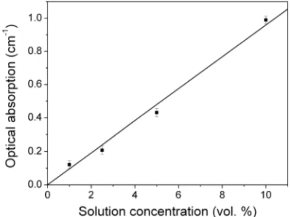
Figure 6 plots the optical absorption of N-methylaniline solutions with different concentrations, measured using the optofluidic resonator. The lowest concentration we test in our experiment is 1%, which corresponds to ~ 0.1 cm-1
absorption coefficient. To evaluate the absorption detection limit of the device, we performed multiple measurements and the standard deviation of the resulting data is taken as the noise floor of our experimental setup. If we define the detection limit as the solution optical absorption that generates a signal-to-noise ratio of unity, the detection limit of a resonator with 17.2 dB extinction ratio (Fig. 5) is approximately 0.02 cm-1 based on experimentally determined noise
total integration time of 0.6 s. The 0.02 cm-1 detection limit is in good agreement with the theoretically simulated value
of 0.016 cm-1, using a Monte-Carlo method10.
Figure 6. Measured optical absorption of methylaniline solutions in carbon tetrachloride as a function of N-methylaniline concentration near the wavelength of 1500 nm.
5. MICRO-CAVITY PHOTOTHERMAL SENSOR
Both of the former two techniques we discussed rely on direct measurement of optical attenuation induced by molecular absorption. Indirect absorbance measurement techniques have also been implemented to overcome certain limitations of direct absorbance sensing methods. Among them, PhotoThermal Spectroscopy (PTS) has been recognized as a highly sensitive and precise method for measuring infrared molecular absorption. Its competitive advantages over direct absorbance measurement are two-fold: immunity to scattering interference and improved sensitivity/accuracy. Since optical scattering/reflection does not generate a photothermal signal, PTS is particularly suitable for field applications where scattering is often a major concern22. For example, PTS has been successfully applied to aerosol absorption
measurement where optical scattering almost completely overshadows optical absorption23. In addition to its immunity
to scattering interference, the measured optical signal can be amplified by photothermal effects in PTS. Such amplification is quantified using an enhancement factor, defined as the ratio of optical signal magnitudes caused by photothermal effects and by direct absorption24. Enhancement factors up to ~ 2000 with respect to conventional
transmission-based IR spectroscopy have been experimentally demonstrated, making PTS a highly sensitive technique for trace chemical analysis25.
The sensitivity of the PTS technique can be further improved by introduction of optical resonant cavity enhancement. We have theoretically analyzed the performance of examine a new Micro-Cavity PhotoThermal Spectroscopy (MC-PTS) technique, where the conventional etalon cavity consisting of bulk mirror assembly is substituted by a micro-cavity such as microsphere, micro-ring or micro-disk. In MC-PTS, both the pump and probe light can be tuned to resonate inside the micro-cavity and maximize their optical mode spatial overlap. As a consequence of such a doubly-resonant configuration, both the optical absorption process of the pump beam and the thermal amplification enhancement factor are maximized, which in turn leads to very high absorption detection sensitivity. Moreover, whereas the photothermal enhancement factor of conventional PTS techniques is limited by the optical and thermal properties of sample materials, the thermal properties of micro-cavities used in MC-PTS can be engineered through material and geometry design to achieve record large photothermal enhancement factors. Additional benefits of using a micro-cavity include short response time due to its small thermal mass (which also helps to reduce 1/f noise by using high frequency chopped measurement), device miniaturization, elimination of complicated alignment, reduced ambient turbulence by micro-environment control, and the possibility of planar integration with other photonic or electronic components.
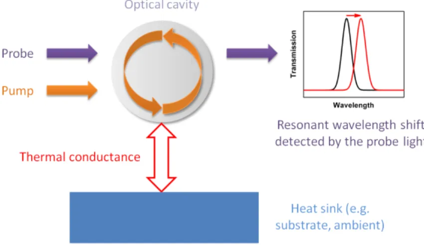
The generic pump-probe configuration of an MC-PTS device is illustrated in Fig. 7. The core component of the device is an optical cavity, which in the most general case can either be a traveling wave cavity such as ring, micro-disk or micro-sphere, or a standing wave cavity such as a multi-layer Bragg cavity or a point defect in a photonic crystal slab. The cavity is thermally connected to a heat sink (e.g. the substrate on which the micro-cavity device is fabricated) through a thermal conductance G. Given its large thermal mass, the heat sink may be regarded to be held at a constant
temperature T0, which will be used as a reference point for the temperature rise in the micro-cavity. In the pump-probe
configuration, a high-power pump beam is actively locked to one of the resonant frequencies of the cavity through a feedback loop which monitors the transmitted intensity in real-time, and is used to induce optical absorption and photothermal effects in the cavity. When optically absorbing molecules are present in the ambient surrounding the cavity, the optical resonant mode of the pump beam interacts with these molecular species evanescently: such interaction converts optical energy of the pump beam into heat via optical absorption. Consequently, the temperature of the cavity will increase from T0 to T0 + dT when thermal equilibrium is established between the photothermal heat generation and
heat dissipation through the thermal conductance. The resulting temperature change dT translates to a cavity resonant wavelength change dλp due to thermo-optic effect:
dT
d
λ
p=
κ
⋅
(2)where κ is the thermo-optic coefficient of the micro-cavity (the subscript p following λ denotes that the wavelength λp is
associated with the probe beam). Such a resonant wavelength shift is then detected by a low-power probe beam using wavelength or intensity interrogation.
Figure 7. Illustration of the generic configuration of a micro-cavity device for MC-PTS.
Using the generic model shown in Fig. 7, we derived the photothermal enhancement factor of a micro-cavity with a heat capacity C measured using a sinusoidal input at a frequency f to be9:
PQ f G n n f E f E p c ⋅ + Γ ⋅ = + = 2 2 2 2 2 2 32 1 4 3 3 4 1 ) 0 ( ) ( τ π λ κ τ π (3)
where E(0) is the photothermal enhancement factor at zero frequency, n is the index of refraction (real part) of the sensing medium surrounding the cavity, Q is the cavity quality factor, P is the pump light power coupled into the cavity, nc denotes refractive index of the cavity material, τ = C/G is the thermal time constant of the micro-cavity, and Γ is the
fractional cavity modal confinement in the surrounding medium where the target molecular species is present. The contribution of cavity enhancement effect to the photothermal signal dIp is two-fold: the optical absorption of the pump
and hence photothermal heat generation is enhanced roughly by a factor of Q; and the resonant peak width is inversely proportional to Q such that even a small resonant wavelength shift dλp translates to a large probe intensity change which
is increased by a factor of Q, leading to another factor of Q boost. Eq. (4) suggests that the enhancement factor is proportional to the cavity Q-factor. This is also consistent with previous analysis by other authors27. Therefore, we can
expect very large photothermal enhancement with respect to conventional cavity-enhanced absorption spectroscopy by using a high-Q micro-cavity for MC-PTS.
According to Eq. (2), a resonant cavity with high thermo-optic coefficient translates the photothermal temperature rise into large refractive index change and hence large resonant wavelength spectral shift, giving rise to sensitive detection. The resonant cavity also need to be thermally isolated from its environment (i.e. minimize G in Eq. 3) to maximize the temperature change due to absorption. Based on the considerations, a Figure-Of-Merit (FOM) can be defined to quantify the thermal/optical properties of cavity materials:
σ
α
=
FOM
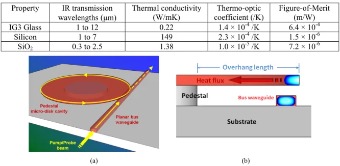
(3)where α is the thermo-optic coefficient and σ denotes the thermal conductivity. This FOM is approximately proportional to the photothermal enhancement factor achievable in cavities made of different materials. We have identified chalcogenide glasses to be an ideal material candidate for nano-cavity photothermal spectroscopy due to their wide optical transparency and superior thermal/optical properties. Table 1 lists the relevant physical properties required for MC-PTS sensing. Here, data for IG3 infrared chalcogenide glass is shown as an example of chalcogenide glass materials26, along with those of silicon and silica (SiO
2) for comparison. Clearly, the material FOM of the commercially
available, unoptimized IG3 chalcogenide glass is almost 100 times that of silica, and over 400 times that of silicon! Table 1. Properties of IG3 chalcogenide glass, Si and SiO2 relevant to micro-cavity photothermal applications
Property IR transmission wavelengths (μm) Thermal conductivity (W/mK) Thermo-optic coefficient (/K) Figure-of-Merit (m/W) IG3 Glass 1 to 12 0.22 1.4 × 10⁻⁴ /K 6.4 × 10⁻⁴ Silicon 1 to 7 149 2.3 × 10⁻⁴ /K 1.5 × 10⁻⁶ SiO2 0.3 to 2.5 1.38 1.0 × 10⁻⁵ /K 7.2 × 10⁻⁶ (a) (b)
Figure 8. (a) Schematic tilted view of an on-chip pedestal micro-disk cavity made of chalcogenide glass for MC-PTS applications; (b) cross-section of the pedestal micro-disk cavity (not to scale).
Figures 8(a) and 8(b) show schematic diagrams of the proposed chalcogenide glass micro-cavity device for MC-PTS applications. The device consists of a micro-disk cavity (resonator) made of IG3 glass, a pedestal which mechanically supports the suspended micro-disk cavity, and a planar bus waveguide on the substrate to evanescently couple the pump and probe beams into the cavity. If we assume both pump and probe wavelengths to be around 4 μm, the overhang length to be 10 μm (Fig. 3b), and the micro-disk thickness and diameter to be 1 μm and 100 μm, respectively, we can calculated the photothermal enhancement factor at steady state (f = 0) to be:
) ( 48 . 0 4 3 3 ) 0 ( = ⋅ Γ ⋅PQ=PQ⋅ W−1 G E p λ κ (4)
The time constant of the photothermal signal is τ = C/G ~ 4 × 10⁻⁵ s, corresponding to a nearly flat sensor response up to
measurement frequencies of ~ 10 kHz. Eq. (19) suggests that even for a moderate cavity Q-factor of 2 × 10⁵ and a pump
laser power of 100 mW, a photothermal enhancement factor as large as 104 is expected with respect to direct
cavity-enhanced infrared absorbance measurement we discussed in section 4. Assuming a measurement bandwidth window of 1 Hz, Eq. (4) predicts an absorption detection limit of 2 × 10⁻⁹ cm-1, primarily limited by the heat sink thermal noise.
Therefore, for a pure analyte gas with an infrared absorption coefficient of 50 cm-1 (a typical value for chemical vapors
at room temperature and one atmosphere pressure), the concentration detection limit of the proposed MC-PTS device is ~ 40 ppt (parts-per-trillion). We note that no pre-concentration is yet assumed in deriving this detection limit number; thus orders of magnitude further improvement is expected when the MC-PTS technique is coupled with gas pre-concentration schemes, which will bring the limit of detection well into the sub-ppt range.Such performance qualifies this technique as one of the most sensitive methods for chemical vapor spectroscopic analysis.
6. SUMMARY
In this paper, we have discussed three types of chalcogenide glass-based on-chip optical chemical sensors: waveguide evanescent sensors, micro-disk cavity-enhanced sensors and micro-cavity photothermal sensors, which show progressive performance improvement. We demonstrated that compact, robust, high sensitivity devices can be utilized in liquid/vapor phase sensing devices for infrared spectroscopy and chemical sensing.
Funding support has been provided by the Department of Energy under award number DE-SC52-06NA27341, and the start-up package from the University of Delaware. The authors also acknowledge the Center of Materials Science and Engineering and the Micro-systems Technology Laboratories at MIT for characterization and fabrication facilities.
REFERENCES
[1] P. Yager, T. Edwards, E. Fu, K. Helton, K. Nelson, M. Tam, B. Weigl, “Micro-fluidic diagnostic
technologies for global public health,” Nature 442, 412-418 (2006).
[2] G. Moore, "Cramming more components onto integrated circuits,” Electronics 38, 114 (1965).
[3] A. Marie-Laure, K. Julie, N. Virginie, H. Koji, I. Satoru, B. Catherine, L. Herve, C. Joel, Y. Kiyoyuki, L. Olivier, L. Jenny, C. Florent, C. Chantal, B. Bruno, "Chalcogenide Glass Optical Waveguides for Infrared Biosensing," Sensors 9, 7398-7411 (2009).
[4] P. Lucas, M. Riley, C. Boussard-Pledel, B. Bureau, "Advances in chalcogenide fiber evanescent wave biochemical sensing," Anal. Biochem. 351, 1-10 (2006).
[5] A. Ganjoo, H. Jain, C. Yu, J. Irudayaraj and C. Pantano, “Detection and fingerprinting of pathogens: Mid-IR biosensor using amorphous chalcogenide films,” J. Non-Cryst. Solids 354, 2757-2762 (2008).
[6] N. Hô, M. Phillips, H. Qiao, P. Allen, K. Krishnaswami, B. Riley, T. Myers, and N. Anheier, “Single-mode low-loss chalcogenide glass waveguides for the mid-infrared,” Opt. Lett. 31, 1860-1862, (2006).
[7] S. Hocdé, O. Loréal, O. Sire, C. Boussard-Plédel, B. Bureau, B. Turlin, J. Keirsse, P. Leroyer, and J. Lucas, “Metabolic imaging of tissues by infrared fiber-optic spectroscopy: an efficient tool for medical diagnosis,” J. Biomed. Opt. 9, 404 (2004).
[8] J. Hu, X. Sun, A. Agarwal, and L. C. Kimerling, “Design guidelines for optical resonator biochemical sensors,” J. Opt. Soc. Am. B. 26, 1032-1041 (2009).
[9] J. Hu, “Ultra-sensitive chemical vapor detection using micro-cavity photothermal spectroscopy,” Opt. Express 18, 22174-22186 (2010).
[10] J. Hu, N. Carlie, L. Petit, A. Agarwal, K. Richardson, and L. C. Kimerling, “Cavity-enhanced infrared absorption in planar chalcogenide glass resonators: experiment & analysis,” J. Lightwave Technol. 27, 5240-5245 (2009).
[11] J. Hu, N. Carlie, N. Feng, L. Petit, A. Agarwal, K. Richardson, and L. C. Kimerling, “Planar waveguide-coupled, high-index-contrast, high-Q resonators in chalcogenide glass for sensing,” Opt. Lett. 33, 2500-2502 (2008).
[12] J. Hu, N. Carlie, L. Petit, A. Agarwal, K. Richardson, and L. C. Kimerling, “Demonstration of chalcogenide glass racetrack micro-resonators,” Opt. Lett. 33, 761-763 (2008).
[13] J. Hu, V. Tarasov, N. Carlie, N. Feng, L. Petit, A. Agarwal, K. Richardson, and L. C. Kimerling, “Si-CMOS-compatible lift-off fabrication of low-loss planar chalcogenide waveguides,” Opt. Express 15, 11798-11807 (2007). [14] J. Hu, N. Feng, N. Carlie, L. Petit, A. Agarwal, K. Richardson, and L. C. Kimerling, “Optical loss reduction in
high-index-contrast chalcogenide glass waveguides via thermal reflow,” Opt. Express 18, 1469-1478 (2010).
[15] K. Richardson, L. Petit, N. Carlie, B. Zdyrko, I. Luzinov, J. Hu, A. Agarwal, L. C. Kimerling, T. Anderson, and M. Richardson, “Progress on the fabrication of on-chip, integrated chalcogenide glass (ChG)-based sensors,” J. Nonlinear Opt. Phys. Mater. 19, 75-99 (2010).
[16] L. Petit, N. Carlie, F. Adamietz, M. Couzi, V. Rodriguez, and K. C. Richardson, “Correlation between physical, optical and structural properties of sulfide glasses in the system Ge-Sb-S,” Mater. Chem. Phys. 97, 64-70 (2006). [17] R. Siebert and J. Muller, "Infrared integrated optical evanescent field sensor for gas analysis Part I: System design,"
Sensors Actuat. A 119, 138-149 (2005).
[18] A. Nitkowski, L. Chen, and M. Lipson, “Cavity-enhanced on-chip absorption spectroscopy using microring resonators,” Opt. Express 16, 11930-11936 (2008).
[19] J. Nadeau, V. Ilchenko, D. Kossokovski, G. Bearman and L. Maleki, “High-Q whispering-gallery mode sensor in liquids,” Proc. SPIE 4629, 172-180 (2002).
[20] G. Farca, S. Shopova, and A. Rosenberger, “Cavity-enhanced laser absorption spectroscopy using microresonator whispering-gallery modes,” Opt. Express 15, 17443-17448 (2007).
[21] T. McGarvey, A. Conjusteau and H. Mabuchi, “Finesse and sensitivity gain in cavity-enhanced absorption spectroscopy of biomolecules in solution,” Opt. Express 14, 10441-10451 (2006).
[22] S. E. Bialkowski, “Photothermal Spectroscopy Methods for Chemical Analysis,” in Chemical Analysis: A Series of Monographs on Analytical Chemistry and Its Applications, J. D. Winefordner, ed. (John Wiley & Sons 1996). [23] A. Sedlacek and J. Lee, “Photothermal interferometric aerosol absorption spectrometry,” Aerosol Sci. Technol. 41,
1089-1101 (2007).
[24] N. Dovichi and J. Harris, “Laser Induced Thermal Lens Effect for Calorimetric Trace Analysis,” Anal. Chem. 51, 728-731 (1979).
[25] C. Davis and S. Petuchowski, “Phase fluctuation optical heterodyne spectroscopy of gases,” Appl. Opt. 20, 2539-2554 (1981).
[26] SCHOTT North America Inc., “Infrared Chalcogenide Glass IG3”
[27] A. Armani, R. Kulkarni, S. Fraser, R. Flagan, K. Vahala, “Label-Free, Single-Molecule Detection with Optical Microcavities,” Science 317, 783-787 (2007).