HAL Id: hal-01843394
https://hal.archives-ouvertes.fr/hal-01843394
Submitted on 18 Jul 2018HAL is a multi-disciplinary open access
archive for the deposit and dissemination of sci-entific research documents, whether they are pub-lished or not. The documents may come from teaching and research institutions in France or abroad, or from public or private research centers.
L’archive ouverte pluridisciplinaire HAL, est destinée au dépôt et à la diffusion de documents scientifiques de niveau recherche, publiés ou non, émanant des établissements d’enseignement et de recherche français ou étrangers, des laboratoires publics ou privés.
Novel 3D back-to-back diodes ESD protection
Bertrand Courivaud, Nicolas Nolhier, G. Ferru, Marise Bafleur, Fabrice
Caignet
To cite this version:
Bertrand Courivaud, Nicolas Nolhier, G. Ferru, Marise Bafleur, Fabrice Caignet. Novel 3D back-to-back diodes ESD protection. International ESD Workshop (IEW) , May 2014, Villard de Lans, France. 2p. �hal-01843394�
&
Novel 3D back-to-back diodes ESD protection
B.Courivaud (1,2,3), N.Nolhier (2,3), G.Ferru (1), M.Bafleur (2,3), F.Caignet (2,3)
(1) IPDIA; 2 Rue de la girafe, 14000 Caen FRANCE
(2) CNRS-LAAS; 7 Avenue du Colonel Roche, F-31077 Toulouse, France (3) Université de Toulouse; UPS, INSA, INP, ISAE, LAAS, F-31077 Toulouse, France
A 3D technology is used to design ESD protection devices. These planar bidirectional components, based on back-to-back diodes, are dedicated to first stage, external ESD protection. The main trick consists in using deep trenches, usually employed to perform capacitors, to design 3D diode. These devices should be robust as existing two-dimensional structures regarding ESD stress for a significant area reduction. The specific trench configuration should improve cumulative ESD stress robustness.
I. Introduction
Close to the application where external ESD protection is integrated, its surface aera should be minimized. The main goal of this study is to demonstrate the functionality of 3D diode as ESD protection and to estimate the impact of surface reduction regarding conventional diodes. The technology process is based on an existing one are developed by IPDIA company [1][2] for the design of high values capacitors. During an etch step, we can make some holes in the silicon and after filling them with polysilicon. In this particular case, the deposed polysilicon is doped with high phosphorus active concentration. After a thermal diffusion, we obtain a three dimensional diode including as several holes connected in parallel. Back to back diodes is obtained by duplicate the 3D diode as depicted in Figure 1.
Figure 1: Scheme of 3D back-to-back diodes. The back-to-back configuration deviates the ESD current when the voltage at the protection electrode exceeds their threshold voltage. A typical electrical implantation scheme is shown on Figure2. The component is fully symmetrical i.e. the device
protection is guaranteed for positive and negative ESD discharge.
Figure 1: Typical implementation of external 3D back-to-back diode protection
Clamping voltage requirement is tuned in the range of 10 to 80V regarding technological parameters.
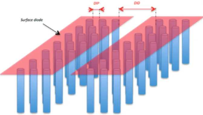
II. Layout parameter variations
In order to optimize ESD protection robustness we have studied two layout parameters, the distance (DIP) between the holes and the distance between the two diodes (DID). As we decided to keep the same active surface area for each diode, lower the distance between holes, involve an increase of their quantity (310 to 5700). A first study was carried out to determine the impact of this parameter on the breakdown voltage. Then, observing Figure 3, we can see that regardless of the number of holes, the leakage current are very steady an the breakdown voltage is slightly the same (19V).The second parameter variation is the distance DID. As shown in Figure 4, DID have been ranged between
&
35 to 165µm. Even if enlarge this distance consume more silicon surface area, we assume that an impact on current homogeneity could be found.
Figure 3: DC curves for several DIP lengths.
Figure 4: Layout of device with DID variation As previous case, for all these devices no significant breakdown voltage variations have been exhibited.
III. Results
To study the device ESD robustness, we perform a Transmission Line Pulsing characterization (TLP). The TLP stresses are increased until the device exhibits a significant leakage current, corresponding to IT2. From the measured results presented in Figure
5, we can observe that the IT2 point increases with the
number of holes. For large DIP distance, each hole can be considered as a elementary diode, so when more and more holes are used, the current density in each hole is lowered, and the ESD robustness is improved. This behaviour is saturating when the number of holes becomes important because the hole’s diffusions touch themselves, creating a mega junction. The results demonstrate that the inter-diode distance DID is also impacting the structure ESD robustness. When DID is increased, the intrinsic resistance of the device is increased too, which should degrade ESD robustness in terms of power dissipation. But, as this added resistance acts as a ballast resistance, the resulting on-resistance of the device during ESD, is lowered because the triggering
of the device is more uniform. DID value has an optimum. A good trade-off between ESD robustness and surface area is found for a device formed by 5700 holes with a 95µm DID length. IT2 is 22A,
corresponding for a rough estimation of 33kV HBM robustness.
Figure 5: TLP curves : IT2 versus number of
holes for different DID values.
However in a specific combination of DID and DIP values, the device exhibits an amazing behaviour. Figure 6 shows that at high current stress of 10A, a first hole is damaged. But as the holes are in parallel, this latter blows-up, and the rest of the structure is still functional up to 16A with a reasonable leakage current (below 1µA). We are investigating this phenomena regard for cumulative ESD stress robustness.
Figure 6: showing small impact of failed holes on the increasing leakage current.
References
[1] F. Murray, “Silicon based system-in-package: a passive integration technology combined with advanced packaging and system based design tools to allow a breakthrough in miniaturization”, BCTM Santa Barbara USA, pp. 169-173, 2005.
[2] S. Gaborieau, C. Bunel, F. Murray, “3D Passive Integrated Capacitors Towards Even Higher Integration”, 6th International Conference and Exhibition on Device Packaging, Fountain Hills(AZ), 2010