Publisher’s version / Version de l'éditeur:
Langmuir, 32, 23, pp. 5890-5898, 2016-05-18
READ THESE TERMS AND CONDITIONS CAREFULLY BEFORE USING THIS WEBSITE.
https://nrc-publications.canada.ca/eng/copyright
Vous avez des questions? Nous pouvons vous aider. Pour communiquer directement avec un auteur, consultez la première page de la revue dans laquelle son article a été publié afin de trouver ses coordonnées. Si vous n’arrivez pas à les repérer, communiquez avec nous à [email protected].
Questions? Contact the NRC Publications Archive team at
[email protected]. If you wish to email the authors directly, please see the first page of the publication for their contact information.
NRC Publications Archive
Archives des publications du CNRC
This publication could be one of several versions: author’s original, accepted manuscript or the publisher’s version. / La version de cette publication peut être l’une des suivantes : la version prépublication de l’auteur, la version acceptée du manuscrit ou la version de l’éditeur.
For the publisher’s version, please access the DOI link below./ Pour consulter la version de l’éditeur, utilisez le lien DOI ci-dessous.
https://doi.org/10.1021/acs.langmuir.6b01365
Access and use of this website and the material on it are subject to the Terms and Conditions set forth at
Sequential nanopatterned block copolymer self-assembly on surfaces
Jin, Cong; Olsen, Brian C.; Wu, Nathanael L. Y.; Luber, Erik J.; Buriak, Jillian
M.
https://publications-cnrc.canada.ca/fra/droits
L’accès à ce site Web et l’utilisation de son contenu sont assujettis aux conditions présentées dans le site LISEZ CES CONDITIONS ATTENTIVEMENT AVANT D’UTILISER CE SITE WEB.
NRC Publications Record / Notice d'Archives des publications de CNRC:
https://nrc-publications.canada.ca/eng/view/object/?id=ae78d03e-4423-4de5-89fb-823bb3c0676b https://publications-cnrc.canada.ca/fra/voir/objet/?id=ae78d03e-4423-4de5-89fb-823bb3c0676b
Sequential Nanopatterned Block Copolymer Self-Assembly on
Surfaces
Cong Jin,
†,‡Brian C. Olsen,
†,‡Nathanael L. Y. Wu,
‡,§Erik J. Luber,
*
,†,‡and Jillian M. Buriak
*
,†,‡†
Department of Chemistry, University of Alberta, 11227 Saskatchewan Drive, Edmonton, AB T6G 2G2, Canada ‡
National Institute for Nanotechnology, National Research Council Canada, 11421 Saskatchewan Drive, Edmonton, AB T6G 2M9, Canada
§
Department of Electrical and Computer Engineering, University of Alberta, Edmonton, Alberta T6G 2G8, Canada
*
S Supporting InformationABSTRACT: Bottom-up self-assembly of high-density block-copolymer nanopatterns is of significant interest for a range of technologies, including memory storage and low-cost lithog-raphy for on-chip applications. The intrinsic or native spacing of a given block copolymer is dependent upon its size (N, degree of polymerization), composition, and the conditions of self-assembly. Polystyrene-block-polydimethylsiloxane (PS-b-PDMS) block copolymers, which are well-established for the production of strongly segregated single-layer hexagonal nano-patterns of silica dots, can be layered sequentially to produce density-doubled and -tripled nanopatterns. The center-to-center spacing and diameter of the resulting silica dots are
critical with respect to the resulting double- and triple-layer assemblies because dot overlap reduces the quality of the resulting pattern. The addition of polystyrene (PS) homopolymer to PS-b-PDMS reduces the size of the resulting silica dots but leads to increased disorder at higher concentrations. The quality of these density-multiplied patterns can be calculated and predicted using parameters easily derived from SEM micrographs of corresponding single and multilayer patterns; simple geometric considerations underlie the degree of overlap of dots and layer-to-layer registration, two important factors for regular ordered patterns, and clearly defined dot borders. Because the higher-molecular-weight block copolymers tend to yield more regular patterns than smaller block copolymers, as defined by order and dot circularity, this sequential patterning approach may provide a route toward harnessing these materials, thus surpassing their native feature density.
■
INTRODUCTIONSignificant advances in the self-assembly of block copolymers (BCPs) on surfaces have yielded a remarkable diversity of highly complex nanopatterns.1−11As a result, self-assembly has been identified as a viable approach for rapid parallel nano-patterning of technologically relevant semiconductor surfaces for on-chip information storage.12−18For a given thin-film BCP, the resulting nanopattern is determined by the material constraints of the polymer and the processing conditions.19 Significant efforts have focused on the production of high-density nanopatterns with sub-20-nm spacing, with great atten-tion devoted to the development of small diblock copolymers comprising two immiscible blocks, as defined by a large (positive) Flory−Huggins interaction parameter, χ.6,20−24 Because the spacing of a given self-assembled BCP nanopattern is generally dependent upon its degree of polymerization, N, the segregation strength of a polymer depends on the product χN; the self-assembly of high-density nanopatterns therefore requires BCPs with higher χ to offset the lower N.25 Recently, the
development of BCPs with small N and large χ has proven to be a fruitful approach toward making high-density BCP arrays.22−24,26
Without the use of lithographically defined guiding features or
prepatterned substrates, however, well-defined control and im-plementation of these new polymers as templates for high-fidelity pattern transfer is challenging, in part due to reduced segregation of the two short blocks.27,28
Here we describe a fully bottom-up approach that attempts to surpass the intrinsic, or native, density of a given single-layer nanopattern of dots using strongly segregating BCPs that yield ordered nanopatterns over large areas. Through two or three identical self-assembly steps, density-doubled or density-tripled nanopatterns, respectively, can be accessed. The processing for each layer is straightforward and repetitive, which simplifies the overall procedure. The concept of density multiplication of BCP-based self-assembly has seen some attention, as summar-ized by four examples. Spatz and co-workers used a two-step BCP-based approach for making mixed-metal gold and titania hexagonal dot arrangements.29Kim and co-workers showed that metal dot-and-line patterns produced from BCP self-assembly could be treated with a second BCP self-assembly step to Received: April 9, 2016
Revised: May 17, 2016 Published: May 18, 2016
produce more complex patterns, and although the results are very promising, detailed quantification and analysis was not carried out.30 A one-step conversion of a BCP bilayer into density-doubled dots has also been shown by Wu and co-workers, but the results may not be generalizable as they are complicated by nonuniform dot heights and sizes.31 Line frequency doubling of
BCP-derived nanostructures has also been demonstrated via application of a self-aligned doubled patterning (SADP) process to produce density-doubled metal lines.32 In this work, we demonstrate the sequential patterning of highly ordered silica dot patterns to yield density-doubled and -tripled dot patterns, derived from a well-established family of high-χ BCPs, PS-b-PDMS (polystyrene-block-polydimethylsiloxane). The spacing of the hexagonal nanopatterns was systematically tuned, and the quality of these density-multiplied patterns, measured as the fraction of dots that are distinct and separate, was fully quantified and modeled.
■
EXPERIMENTAL SECTIONMaterials. PS-b-PDMS (31K−14.5K, 43K−8.5K, 22.5K−4.5K, and 34K−5.5K) and polystyrene (PS) (Mn = 10K g/mol and
Mn = 5K g/mol) were purchased from Polymer Source Inc. The polydispersity index (PDI), as measured by size exclusion chromatog-raphy (SEC) of PS-b-PDMS (31K−14.5K), PS-b-PDMS (43K−8.5K), PS-b-PDMS (22.5K−4.5K), and PS-b-PDMS (34k−5.5k) were 1.15, 1.04, 1.09, and 1.09, respectively (data provided by the Polymer Source Inc., for the specific batches); sulfuric acid (96%) and hydrogen peroxide (30%) were purchased from Avantor Performance Materials, Inc.; toluene and THF were obtained from Fisher Scientific; and silicon wafers (⟨100⟩, thickness: 525 ± 25 μm) were obtained from WRS Materials.
Dicing.Silicon wafers were cut into 1 cm × 1 cm squares with a dicing saw (Disco DAD 321).
Substrate and Sample Cleaning. Diced silicon wafers and samples after the first or second annealing and etching steps were cleaned using piranha solution [3:1 v/v sulfuric acid (96%)/hydrogen peroxide (30%)]. Substrates and samples were immersed in a piranha solution for 15 min, rinsed with DI water, and dried in a stream of nitrogen.
Figure 1.Sequential self-assembly process. (a) Schematic of sequential layer deposition: a single-layer hexagonal dot pattern (blue) is deposited via spin casting of a BCP thin film, followed by annealing and plasma treatment. A second layer (green) is then deposited via the same process to form a honeycomb dot pattern. Finally, a third layer of BCP (yellow) is deposited on top of the honeycomb dot pattern, resulting in a triple-density hexagonal dot pattern. Plan-view and tilted SEM micrographs of PS-b-PDMS (31K−14.5K, blended with 30 wt % PS) (b, c) single layer, (d, e) double layer, and (f, g) triple-layer dot patterns. All scale bars are 250 nm.
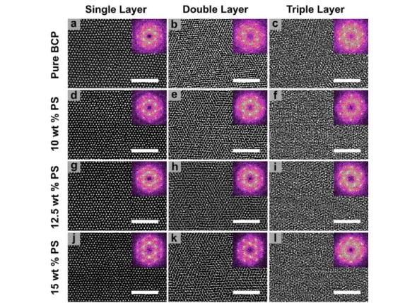
Figure 2.Plan-view SEM micrographs of single-, double-, and triple-layer nanopatterns formed from PS-b-PDMS (22.5K−4.5K), blended with different quantities of PS (5K). (a−c) Neat-b-PDMS (22.5K−4.5K). (d−f) 10 wt % PS (5K). (g−i) 12.5 wt % of PS (5K). (j−l) 15 wt % PS (5K). All scale bars are 250 nm.
Langmuir Article
DOI:10.1021/acs.langmuir.6b01365
Langmuir2016, 32, 5890−5898 5891
BCP Thin-Film Self-Assembly. Individual solutions of PS-b-PDMS (31K−14.5K), PS-b-PS-b-PDMS (43K−8.5K), PS-b-PS-b-PDMS (34K− 5.5K), PS-b-PDMS (22.5K−4.5K), and PS (Mn= 10 000 g/mol,
M = 5000 g/mol) were prepared by dissolution in toluene to make 1 wt % solutions. For solutions of mixtures of polymers, PS-b-PDMS (22.5K−4.5K, 1 wt %) was mixed with PS (Mn= 5000 g/mol, 1 wt %) at 10, 12.5, 15, 17.5, 20, and 30% fractions of the total polymer weight. PS-b-PDMS (31K−14.5K, 1 wt %) was mixed with PS (Mn= 10K g/mol, 1 wt %) at 30, 40, and 50% fractions of the total polymer weight. PS-b-PDMS (34K−5.5K, 1 wt %) was mixed with PS (Mn= 10K g/mol, 1 wt %) at a 15% fraction of the total polymer weight. Block copolymer blends were stirred for 24 h before use. The polymer solution (17 μL) was spin-coated (model WS-400BZ-6NPP/ LITE spin-coater, Laurell Technologies Corporation) on a piranha-solution-cleaned silicon substrate. Detailed spin-coating conditions for
each BCP or BCP blend are listed inTable S1. In addition, the film thickness of each case was measured with ellipsometry, and the results are also summarized inTable S1. These as-cast samples were then placed in a custom-designed chamber for solvent annealing in THF vapor (chamber details inFigure S1), in which the film thickness was measured in situ by ellipsometry. To determine the best solvent annealing conditions for each different type of BCP, for a given initial thickness, the swelling ratios of the films during annealing were adjusted by varying the steady-state vapor pressure of THF in the chamber. The THF vapor pressure was controlled by filling different combinations of solvent reservoirs with THF, allowing the solvent surface area (and consequent vapor pressure) to be adjusted. The solvent annealing parameters for each BCP and BCP blend are listed inTable S1. This process was found to be consistent and repeatable, as determined by the measured swelling ratios from in situ ellipsometry. Following solvent annealing, the BCP films were converted to SiOxand inspected using
SEM. From these data, the annealing conditions producing the most highly ordered dot arrays were chosen. To clarify, the system was allowed to reach the equilibrium vapor pressure of solvent, which is influenced by the total surface area of filled reservoirs. Thickness monitoring was used to quantitatively monitor the process and determine how long of an annealing was needed for the film to become fully saturated. A typical swelling ratio curve inFigure S2is shown as an example. All solvent annealing was performed at room temperature, but it is noted that long-period fluctuations in the swelling ratio (Figure S2) are a result of room-temperature fluctuations.32Annealed
BCP films were then plasma-etched using a PlasmaLab μETCH. An etching recipe is considered to be good if it yields clean dot patterns and has no underetch (no polymer residue left in between dots) and Figure 3.Higher-contrast and higher-magnification SEM micrographs
of the triple-layer patterns fromFigure 2, formed from (a) PS-b-PDMS (22.5K−4.5K) and (b) PS-b-PDMS (22.5K−4.5K) blended with 15 wt % PS. Scale bars are 100 nm.
Figure 4.(a) Lattice parameter and silica dot diameter versus the percentage of blended PS for PS-b-PDMS (22.5K−4.5K), as calculated from
Figure 2and theSupporting Information. (b) Schematic representation of the BCP micelles upon increasing the weight percentage of added (PS in blue, PDMS in red). (c) The calculated value of β versus the weight percentage of blended PS. (d) Geometric values of interest within a perfect hexagonal lattice, showing three different scenarios of dot-to-dot contact within a lattice, from dot overlap (β > 1) to touching of the edges (β = 1) to no contact (β < 1).
no overetch (clear dot pattern under SEM, not a faint signal). The best etching conditions for each BCP and BCP blend are outlined in
Table S1.
After the preparation of a layer of silica dots, the samples were analyzed by SEM before the preparation of a subsequent layer. After SEM analysis, the sample was first piranha cleaned (vide infra), and then subjected to an identical process to form the next layer. All of the conditions described here are identical for the single-, double-, and triple-layer films; no modifications are needed.
Characterization and Data Processing.All SEM images were taken using a Hitachi S4800 scanning electron microscope at 15 kV, 20 μA. Tilted SEM images were taken at a 70° tilt angle for single-layer samples and 60° for double- and triple-density samples. All SEM micrographs were processed in Gwyddion and ImageJ.
■
RESULTS AND DISCUSSIONA scheme illustrating sequential layer deposition is shown in
Figure 1a. A highly ordered single layer of hexagonally packed dots (Figure 1b,c) was prepared by spin casting a thin film of BCP, PS-b-PDMS (31K−14.5K), blended with 30 wt % PS, onto a native oxide-capped silicon surface. The as-cast film was solvent annealed and plasma treated, resulting in the formation of silica dots on the silicon surface.34 The lattice parameter (the center-to-center spacing) and dot diameter of the resulting silica hexagonal dot pattern are approximately 44.0 and 20.5 nm, respectively. The deposition of a second layer on top of the first layer, using identical processing conditions, results in the formation of a combined dot pattern possessing a honeycomb lattice (Figure 1d,e). The spatial position of the dots in the second layer is coincident with the triangular interstitial
positions of the first layer. The density of the dot pattern can be further increased if a subsequent layer of BCP is deposited on the honeycomb lattice template. The dots of this third layer are registered to the hexagonal lattice positions, forming a triple-density hexagonal lattice dot pattern (Figure 1f,g). Because the surfaces are chemically homogeneous (uniformly SiOx), the
registra-tion is driven by the topology of the resulting dot pattern. The generalization of the approach to a BCP that has approximately half the molecular weight and thus correspond-ing smaller features leads to the formation of the scorrespond-ingle-layer pattern shown inFigure 2a. The lattice parameter for this BCP is 25.1 ± 2.3 nm, with a dot diameter of 12.4 ± 0.9 nm. As can be seen for the double-layer pattern in Figure 2b, there is substantial dot overlap because few of the dots are isolated and distinct. The application of a third layer (Figure 2c) results in a poorly defined pattern due to considerable dot overlap and indistinguishable dot boundaries (vide infra). Fundamental to enabling density multiplication is that the dots derived from the different layers must be spatially separate and distinct from each other.33To try to improve the dot separation, polystyrene (PS, 5K) was added to the PS-b-PDMS (22.5K−4.5K) BCP to increase the notional molecular weight of the PS block.35,36 The effect of added PS on the resulting patterns is summarized in Figure 2d−l. As can be seen upon close inspection, the addition of PS, up to 15 wt % to PS-b-PDMS (22.5K−4.5K) BCP, results in the dots becoming more clearly distinguishable in both the double- and triple-layer patterns. The effect becomes more obvious in the higher-contrast micrographs of the triple-density patterns shown inFigure 3. The triple-layer BCP pattern
Figure 5.Analysis of double-layer dot patterns. (a) SEM micrograph of the double layer honeycomb dot pattern formed via sequential layer deposition of PS-b-PDMS (31K−14.5K) with 30 wt % PS (scale bar = 250 nm), which is separated into (b) individual single-layer patterns, where each dot is colored by its mean hydrostatic strain. The deformation of the local coordination shell is visualized by Voronoi tessellation. (c) Dot pattern in (a) colored by the difference in closest-neighbor center-to-center dot spacing and dot diameter (normalized by the average dot diameter) where overlapping dots are marked with a black border.
Langmuir Article
DOI:10.1021/acs.langmuir.6b01365
Langmuir2016, 32, 5890−5898 5893
with 15 wt % PS (Figure 3b) is more regular with respect to registration and dot separation than the neat PS-b-PDMS (22.5K−4.5K) BCP (Figure 3a) as a result of the subtle decrease in dot size relative to the spacing.
Quantification of the effect of adding PS, within the patterns shown inFigures 2and3, is described inFigure 4. The plots in
Figure 4a,b graphically show the role of added PS on the lattice parameter of the resulting hexagonal nanopattern, as well as the dot diameter. The lattice parameter remains constant over this range of added PS, but the dot diameter decreases as a percentage of added PS homopolymer, from 12.4 ± 0.9 to 10.8 ± 0.9 nm, from 0 to 17.5% added PS, respectively.35,36 Because the same volume of polymer blend in toluene is used to generate the films, the addition of PS results in a decrease in the quantity of PDMS, thus leading to smaller dot diameters. At 20 wt % PS and greater, when added to this BCP, the hexagonal dot patterns become substantially disordered, as shown in theSupporting Information, and thus these patterns were not studied for sequential BCP assembly. For there to be no overlap in a perfect lattice, the value of β, as defined in
Figure 4c,d, needs to be less than 1. Physically, β is the fraction of empty space between a dot residing in the interstitial position of the host hexagonal lattice.Figure 4c shows that β, as calculated from multiple SEM micrographs of hexagonal nanopatterns, decreased with added PS from 0.857 to 0.743. The standard deviations shown inFigure 4c are large and result from considerable fluctuation of the hexagonal dot pattern from a perfect lattice, meaning that a smaller value of β is preferable to allow for additional space, or wiggle room, for the dots within the pattern. As seen inFigures 1−3, the dot patterns formed by BCP self-assembly are not idealized perfect hexagonal lattices because they have point defects (dislocations and vacancies, etc.), grain boundaries, and localized fluctuations from ideal posi-tions.37 If there are sufficiently large positional fluctuations or point defects, then the perfect registration of dots in the upper layer will be compromised, resulting in overlap between dots and a reduction of the maximum achievable density.
Although visual analysis of an SEM micrograph can provide qualitative information regarding the degree of order, a better method to quantify the level of defects and deformation in the observed dot pattern is required to rationally optimize a given system. A formalism of finite strain theory was applied as follows. Briefly, from SEM micrographs of honeycomb dot patterns formed from two layers, the intralayer coordination shell of each dot can be determined by identifying the set of coordinating dots with a minimum centrosymmetry parameter.38 (See the
Supporting Information for more details.) The deviation of each coordination shell, relative to a perfectly regular hexagonal coordination shell, can be quantified via the deformation gradient tensor FN,39which is given by40
∑
∑
= ⊗ ⊗ = − = FN ( d d) ( d d ) i i i i i i N 1 6 0 0 1 1 6 0where diN and di0are the vectors connecting the central dot to
coordinating dots in the deformed and undeformed configura-tions, respectively. Finally, the singular values of FNare used to
calculate the mean hydrostatic strain ϵ̅ of each coordination shell. (See theSupporting Informationfor more details.) It is noted that the hydrostatic strain is simply a measure of how different the local environment of each dot is from a perfect hexagonal lattice.41 This should not be confused with mechanical stress (that results in the deformation of the lattice).
A demonstration of this approach is shown in Figure 5a, an SEM micrograph of a sequentially processed double-layer honeycomb pattern made from a blend of PS-b-PDMS (31K−14.5K) with 30 wt % PS. This BCP has a higher
Figure 6.(a) Map of the predicted dot overlap for double-layer dot patterns as a function of BCP material parameters β and σϵ̅. Contours are separated by 3% overlap, with the lowest contour shown at 1% overlap. (b−e) SEM micrographs (left) of double-layer dot patterns of PS-b-PDMS (31K−14.5K) with varying wt % PS (30, 40, 50) and PS-b-PDMS (43K−8.5K), respectively. Corresponding dot pattern colored by the closest nearest-neighbor distance (right), where overlapping dots are marked with a black border. The β and σϵ̅ parameters for each of these polymers are marked on the dot overlap map in (a), showing the predicted overlap expected for each of these polymers. All scale bars are 250 nm.
molecular weight than the PS-b-PDMS (22.5K−4.5K) used in
Figures 2−4, and the resulting dot pattern is of considerably higher quality. The dots within the pattern in Figure 5a are distinct with little overlap and can be easily differentiated on the basis of their layer of origin (Figure 5b), where each dot is colored by ϵ̅ and the coordination shell is visualized via Voronoi tessellation. Both layers are highly ordered hexagonal lattices in which each dot has hexagonal intralayer coordination. (It should noted that there is a nonzero point defect density, but in all samples the defect density of the individual single layers is found to be less than 1% of all dots; seeFigure S3). Moreover, both layers possess identical lattice parameters (44.3 ± 0.1 nm), and the distributions of ϵ̅ for each layer (Figure S4a,b) are both found to be Gaussian (seeFigure S5for large scale statistics), with a standard deviation ofσ
ϵ̅ = 1.8%.
Shown inFigure 5c is a representation of the dot positions in
Figure 5a, where each dot is colored by the difference in closest nearest-neighbor center-to-center dot spacing and dot diameter (normalized by the average dot diameter), where overlapping dots are marked with a black border. Despite both individual layers being highly ordered and parametrically indistinguishable from each other, we see that there is a significant percentage of dots that overlap with dots from another layer (17% dot overlap, where two dots are defined to overlap if their center-to-center distance is less than the average dot diameter).
To approach the theoretical limits for density multiplication via sequential layer deposition, it is necessary to design material systems and methods that minimize the dot overlap between layers. To this end, we have developed an empirical model that can be used to describe and predict the amount of dot overlap produced by the sequential layer deposition of BCP dot patterns. In this model, the amount of dot overlap can be predicted from only two material parameters: the standard deviation in hydrostatic strain,σ
ϵ̅, and the dimensionless constant,
β= √3d0/L0, where d0is the mean dot diameter and L0is the
lattice parameter. From the results shown inFigure 4, it was found that the combined-layer dot pattern could be described by the superposition of two single-layer hexagonal lattices,
where the dots are registered to interstitial positions with a random perturbation set by the value ofσ
ϵ̅. (See theSupporting
Information for simulation details.) The predictions of this model are shown inFigure 6a, which is a contour map of dot overlap as a function of β and σ
ϵ̅. As expected, this model
predicts that the total amount of overlap decreases with both βandσ
ϵ̅.
To validate the predictions of this model, a series of se-quentially deposited honeycomb dot lattices were fabricated using different β and σ
ϵ̅ parameters. These parameters are
systematically varied by adjusting the fraction of polystyrene blended with PS-b-PDMS (31K−14.5K), ranging from 30 wt % PS to 50 wt % PS. The values of β andσ
ϵ̅ and the dot overlap
are measured from the double-layer dot patterns (Figures 6b−e) for each polymer blend. It is found that the measured overlap for each polymer blend agrees within error of the values predicted inFigure 6a (Table 2). Specifically, the overlaps are found to be 17 ± 3, 6 ± 1, and 9 ± 1% for PS fractions of 30, 40, and 50 wt % respectively. The minimal overlap observed
Table 1. Values of Mean Dot Diameter d0, Lattice Parameter
L0, β Parameter, Standard Deviation of Hydrostatic Strain
σ
ϵ̅, Measured Double-Layer Dot Overlap, and Measured
Triple-Layer Dot Overlap for PS-b-PDMS (22.5K−4.5K) and Its PS Blends
added wt % PS to the BCP d0(nm) L0(nm) β σε (%) double-layer overlap (%) triple layer overlap (%) 0 12.4 ± 0.9 25.1 ± 2.3 0.857 2.88 42 64 10 11.5 ± 0.8 25.1 ± 2.2 0.786 2.71 22 37 12.5 11.6 ± 0.9 25.1 ± 2.2 0.780 2.75 21 36 15 11.1 ± 0.8 25.2 ± 2.2 0.762 2.75 18 30 17.5 10.8 ± 0.9 25.2 ± 2.2 0.743 2.82 15 27
Table 2. Values of Mean Dot Diameter d0, Lattice Parameter L0, β Parameter, Standard Deviation of Hydrostatic Strainσ
ϵ̅,
Measured Dot Overlap, and Predicted Dot Overlap for Double-Layer Patterns
BCP blend d0(nm) L0(nm) β σ
ϵ̅(%) measured overlap (%) predicted overlap (%) PS-b-PDMS (31K−14.5K) with 30 wt % PS 20.6 ± 0.5 43.9 0.81 ± 0.02 2.0 17 ± 3 17 ± 2 PS-b-PDMS (31K−14.5K) with 40 wt % PS 18.8 ± 0.5 44.9 0.73 ± 0.02 2.3 6 ± 1 7 ± 1 PS-b-PDMS (31K−14.5K) with 50 wt % PS 17.4 ± 0.5 48.1 0.63 ± 0.02 3.7 9 ± 1 10 ± 1 PS-b-PDMS (43K−8.5K) 14.7 ± 0.5 36.0 0.71 ± 0.02 2.1 3 ± 1 3.0 ± 0.6
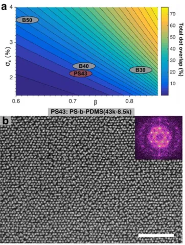
Figure 7. (a) Map of dot overlap for triple-layer dot patterns. Contours are separated by 3% overlap, with the lowest contour shown at 1% overlap. (b) SEM micrograph of a triple-layer dot pattern of PS-b-PDMS (43K−8.5K). Abbreviations PS43, B30, B40, and B50 are defined inFigure 6. The scale bar is 250 nm. Inset: FFT.
Langmuir Article
DOI:10.1021/acs.langmuir.6b01365
Langmuir2016, 32, 5890−5898 5895
at a PS fraction of 40% can be physically understood via an inspection of the SEM micrographs inFigure 6, where it is seen that as the PS fraction becomes too large, the deviation of dots from a perfect hexagonal coordination shell becomes significant and begins to outweigh the increased amount of free space between dots (reduction in β), resulting in a large amount of overlap.
Minimizing the amount of dot overlap is clearly of primary concern when selecting polymers to be used for the fabrication of highly ordered, sequentially deposited dot patterns. However, if this technique is to be used to increase the absolute dot density, then it is also necessary to minimize both dot overlap and the dot pattern lattice parameter. As such, a polymer PS-b-PDMS (43K−8.5K) with a 25% smaller lattice parameter (35.8 ± 0.5 nm) and slightly smaller values of β and σ
ϵ̅
parameters (0.71 ± 0.02 and 2.1 ± 0.1%, respectively) was used for sequential layer deposition instead of PS-b-PDMS (31K−14.5K) with 40 wt % PS. Shown inFigure 6e is an SEM micrograph of a double-layer dot pattern formed via the sequential layer deposition of PS-b-PDMS (43K−8.5K), resulting in a highly ordered lattice with a dot overlap of 3 ± 1% (predicted overlap of 2.9 ± 0.8%). Moreover, the dot density is found to be 1.1 teradots/in2, which is ∼60% greater
than the densities achieved with PS-b-PDMS (31K−14.5K) and 40 wt % PS.
Shown inFigure 7a is the map of predicted overlap for triple-layer dot patterns, which is very similar to the double-triple-layer overlap map, with the primary difference being greater amounts of overlap for identical β andσ
ϵ̅ parameters. As such, given
these stricter requirements on β andσ
ϵ̅, triple-layer dot patterns
are made using PS-b-PDMS (43K−8.5K). The triple-layer dot pattern of PS-b-PDMS (43K−8.5K) is shown in Figure 7b,
which is found to have a 3% defect density, a 13 ± 3% overlap (predicted overlap of 8 ± 3%), and a dot density of 1.58 ± 0.05 Td/in2. An inspection of the FFT (Figure 6b) of this
triple-layer pattern reveals a well-defined spot pattern, indicating long-range periodic ordering. In contrast, the triple-density pattern shown in Figures 2 and 3, formed from the smaller BCP, PS-b-PDMS (22.5K−4.5K), is 64%. The addition of 15 wt % PS, which resulted in smaller dot diameters and a corresponding decrease in β (Figures 2l and3d), led to a lower overlap of 30% in the resulting pattern (Table 1).
To further explore the utility of this density multiplication technique, it was applied to PS-b-PDMS (31K−14.5K) with 15 wt % PS, which has a smaller lattice parameter of 28.1 nm and single-layer parameters of β = 0.72 and σ
ϵ̅ = 2.5%
(predicted overlap of 16 ± 6%), giving a measured single-layer dot density of 0.97 Td/in2 (Figure 8a). These triple-layer
patterns of PS-b-PDMS (31K−14.5K) with 15 wt % PS were found to have a defect density of 17% and a dot density of 1.9 ± 0.2 Td/in2after accounting for 35 ± 6% overlap (Figure 8b).
It is noted that this measured overlap is much larger than the predicted overlap of 16%. An inspection of PS-b-PDMS (34K−5.5K) with 15 wt % PS dot patterns (Figure 8a) reveals that the individual dots are irregularly shaped and noncircular, indicating that further optimization of the solvent annealing conditions need to be performed. The noncircular shape of these dots is quantified by measuring the circularity of the dots, where a perfect circle has circularity of 1 and an infinitely thin rod has a circularity of 0. It is found that the dots of PS-b-PDMS (31K−14.5K) with 15 wt % PS have a mean circularity of 0.78 with a standard deviation of 0.06; when compared to the dots from PS-b-PDMS (43K−8.5K), which have a circularity of 0.86 and a standard deviation of 0.03,
Figure 8.SEM micrographs of (a) single-layer and (b) triple-layer nanopatterns formed using PS-b-PDMS (34K−5.5K) and 15 wt % PS. Inset: FFT. (c) Histograms of dot circularity for single-layer patterns of PS-b-PDMS (43K−8.5K) and PS-b-PDMS (34K−5.5K) with 15 wt % PS. The circularity is calculated as 4π[area]/[perimeter]2. Scale bars are 250 nm.
we see that the dots from PS-b-PDMS (31K−14.5K) with 15 wt % PS are significantly less circular and twice as polydisperse (Figure 8c). As such, the poor circularity and large shape dis-persity is the likely cause for the discrepancy between predicted and observed overlap values because it is assumed in the model that the dots are monodisperse circles.
From the data presented in this work, through the judicious selection of BCP properties and careful optimization of the annealing process,42this density multiplication approach could be a potential approach for surpassing the current density limit of highly ordered dot arrays. Specifically, a reduction in the βparameter could be achieved by tuning the respective volume fractions of each block. For instance, in the case of PS-b-PDMS, increasing the volume fraction of PS to PDMS could reduce the value of β. Furthermore, modifications of the plasma etching procedure could be explored to adjust the value of β and improve the dot height uniformity (seeFigure S6for the AFM micrograph). Second, fluctuations in dot spacing, dot size, and
σ
ϵ̅ result from variations of the BCP film morphology, the
degree of phase separation, and the polydispersity (composition and N) of the BCP.43The polydispersity can be minimized via
synthetic control,44the degree of phase separation is determined by the segregation strength χN, and the BCP film morphology can be contolled by the annealing conditions.45It is also noted that the swelling ratio of the films during the annealing process is subject to room-temperature fluctuations,33where the swelling ratio can change from 1.8 to 2.0 (Figure S2). Therefore, dif-ferences in the swelling ratio of films between subsequent layers may change the dot morphology and spacing. These differences between successive layers will likely degrade the quality of these density-multiplied patterns. As such, improvements in the annealing chamber design, such as temperature control and computer control feedback of solvent vapor flow to maintain a constant swelling ratio, could be used to alleviate this problem to further optimize this approach to density multiplication.46,47
■
CONCLUSIONSIn this work, we suggest a straightforward method for the sequential patterning of BCP hexagonal nanodot arrays using a bottom-up, self-assembly approach. The quality of the resulting patterns is dependent upon the lattice parameter of the hexagonal pattern and the diameter and circularity of the dots, factors that can be controlled via manipulation of the polymer composition and annealing conditions, among others. Given the wide applicability of this method to other dot-forming BCP systems, the density multiplication approach could be extended to other BCP systems, notably, recent efforts toward the synthesis of new families of high X parameter and low N BCPs to yield tightly packed nanopatterned arrays.
■
ASSOCIATED CONTENT*
S Supporting InformationThe Supporting Information is available free of charge on theACS Publications websiteat DOI:10.1021/acs.langmuir.6b01365.
Full details of the annealing chamber used, swelling curves, single-layer defect analysis, grain size, circularity analysis, AFM height maps, algorithms for image dot pattern analysis, quantification of coordination shell, hydrostatic strain calculations, simulation details for generating overlap maps, and single-, double-, and triple-density patterns for all of the BCP films investigated in this work (PDF)
■
AUTHOR INFORMATION Corresponding Authors *E-mail: [email protected]. *E-mail: [email protected]. Author ContributionsC.J. and N.L.Y.W. carried out the experiments. C.J., B.C.O., and E.J.L. analyzed the data. C.J., B.C.O., E.J.L., and J.M.B. wrote the article. All authors have given approval to the final version of the article.
Funding
This work was supported by grants from the Natural Sciences and Engineering Research Council (NSERC, grant numbers RGPIN-283291-09 and RGPIN-2014-05195), Alberta Inno-vates Technology Futures (fellowship to C.J., grant number AITF iCORE IC50-T1 G2013000198), and the Canada Research Chairs program (CRC 207142). Electron microscopy was carried out at NRC-NINT.
Notes
The authors declare no competing financial interest.
■
ACKNOWLEDGMENTSWe are grateful for support from the NSERC, AITF, and the Canada Research Chairs Program. We thank Tate Hauger for assistance with SEM imaging.
■
REFERENCES(1) Darling, S. B. Directing the Self-Assembly of Block Copolymers. Prog. Polym. Sci. 2007, 32, 1152−1204.
(2) Hardy, C. G.; Tang, C. Advances in Square Arrays Through Self-Assembly and Directed Self-Self-Assembly of Block Copolymers. J. Polym. Sci., Part B: Polym. Phys. 2013, 51, 2−15.
(3) Tang, C.; Lennon, E. M.; Fredrickson, G. H.; Kramer, E. J.; Hawker, C. J. Evolution of Block Copolymer Lithography to Highly Ordered Square Arrays. Science 2008, 322, 429−432.
(4) Ruiz, R.; Kang, H.; Detcheverry, F. A.; Dobisz, E.; Kercher, D. S.; Albrecht, T. R.; de, P. J. J.; Nealey, P. F. Density Multiplication and Improved Lithography by Directed Block Copolymer Assembly. Science 2008, 321, 936−939.
(5) Ouk Kim, S.; Solak, H. H.; Stoykovich, M. P.; Ferrier, N. J.; de Pablo, J. J.; Nealey, P. F. Epitaxial Self-Assembly of Block Copolymers on Lithographically Defined Nanopatterned Substrates. Nature 2003, 424, 411−414.
(6) Bita, I.; Yang, J. K. W.; Jung, Y. S.; Ross, C. A.; Thomas, E. L.; Berggren, K. K. Graphoepitaxy of Self-Assembled Block Copolymers on Two-Dimensional Periodic Patterned Templates. Science 2008, 321, 939−943.
(7) Tavakkoli, K. G. A.; Gotrik, K. W.; Hannon, A. F.; Alexander-Katz, A.; Ross, C. A.; Berggren, K. K. Templating Three-Dimensional Self-Assembled Structures in Bilayer Block Copolymer Films. Science 2012, 336, 1294−1298.
(8) Jeong, J. W.; Park, W. I.; Kim, M.-J.; Ross, C. A.; Jung, Y. S. Highly Tunable Self-Assembled Nanostructures from a Poly(2-vinylpyridine-b-dimethylsiloxane) Block Copolymer. Nano Lett. 2011, 11, 4095−4101.
(9) Yager, K. G.; Lai, E.; Black, C. T. Self-Assembled Phases of Block Copolymer Blend Thin Films. ACS Nano 2014, 8, 10582−10588.
(10) Kim, E.; Ahn, H.; Park, S.; Lee, H.; Lee, M.; Lee, S.; Kim, T.; Kwak, E.-A.; Lee, J. H.; Lei, X.; Huh, J.; Bang, J.; Lee, B.; Ryu, Y. D. Directed Assembly of High Molecular Weight Block Copolymers: Highly Ordered Line Patterns of Perpendicularly Oriented Lamellae with Large Periods. ACS Nano 2013, 7, 1952−1960.
(11) Cheng, J. Y.; Rettner, C. T.; Sanders, D. P.; Kim, H.-C.; Hinsberg, W. D. Dense Self-Assembly on Sparse Chemical Patterns: Rectifying and Multiplying Lithographic Patterns Using Block Copolymers. Adv. Mater. 2008, 20, 3155−3158.
Langmuir Article
DOI:10.1021/acs.langmuir.6b01365
Langmuir2016, 32, 5890−5898 5897
(12) Service, R. F. Is the Terabit Within Reach? Science 2006, 314, 1868−1870.
(13) Xiao, S.; Yang, X.; Steiner, P.; Hsu, Y.; Lee, K.; Wago, K.; Kuo, D. Servo-Integrated Patterned Media by Hybrid Directed Self-Assembly. ACS Nano 2014, 8, 11854−11859.
(14) Ruiz, R.; Dobisz, E.; Albrecht, T. R. Rectangular Patterns Using Block Copolymer Directed Assembly for High Bit Aspect Ratio Patterned Media. ACS Nano 2011, 5, 79−84.
(15) Park, M.; Harrison, C.; Chaikin, P. M.; Register, R. A.; Adamson, D. H. Block Copolymer Lithography: Periodic Arrays of ∼ 1011 Holes in 1 Square Centimeter. Science 1997, 276, 1401−1404.
(16) International Technology Roadmap for Semiconductors; Semi-conductor Industry Association: San Jose, CA, 2011.
(17) Herr, D. J. Directed Block Copolymer Self-Assembly for Nanoelectronics Fabrication. J. Mater. Res. 2011, 26, 122−139.
(18) Nunns, A.; Gwyther, J.; Manners, I. Inorganic Block Copolymer Lithography. Polymer 2013, 54, 1269−1284.
(19) Cabrini, S.; Kawata, S. Nanofabrication Handbook; CRC Press, 2012.
(20) Cushen, J. D.; Otsuka, I.; Bates, C. M.; Halila, S.; Fort, S.; Rochas, C.; Easley, J. A.; Rausch, E. L.; Thio, A.; Borsali, R.; Willson, C. G.; Ellison, C. J. Oligosaccharide/Silicon-Containing Block Copolymers with 5 nm Features for Lithographic Applications. ACS Nano 2012, 6, 3424−3433.
(21) Park, S.; Lee, D. H.; Xu, J.; Kim, B.; Hong, S. W.; Jeong, U.; Xu, T.; Russell, T. P. Macroscopic 10-Terabit−per−Square-Inch Arrays from Block Copolymers with Lateral Order. Science 2009, 323, 1030− 1033.
(22) Durand, W. J.; Blachut, G.; Maher, M. J.; Sirard, S.; Tein, S.; Carlson, M. C.; Asano, Y.; Zhou, S. X.; Lane, A. P.; Bates, C. M.; Ellison, C. J.; Willson, C. G. Design of High-χ Block Copolymers for Lithography. J. Polym. Sci., Part A: Polym. Chem. 2015, 53, 344−352. (23) Kennemur, J. G.; Yao, L.; Bates, F. S.; Hillmyer, M. A. Sub-5 Nm Domains in Ordered Poly(cyclohexylethylene)-block-poly(methyl methacrylate) Block Polymers for Lithography. Macromolecules 2014, 47, 1411−1418.
(24) Maher, M. J.; Rettner, C. T.; Bates, C. M.; Blachut, G.; Carlson, M. C.; Durand, W. J.; Ellison, C. J.; Sanders, D. P.; Cheng, J. Y.; Willson, C. G. Directed Self-Assembly of Silicon-Containing Block Copolymer Thin Films. ACS Appl. Mater. Interfaces 2015, 7, 3323− 3328.
(25) Luo, M.; Epps, T. H. Directed Block Copolymer Thin Film Self-Assembly: Emerging Trends in Nanopattern Fabrication. Macro-molecules 2013, 46, 7567−7579.
(26) Bates, C. M.; Seshimo, T.; Maher, M. J.; Durand, W. J.; Cushen, J. D.; Dean, L. M.; Blachut, G.; Ellison, C. J.; Willson, C. G. Polarity-Switching Top Coats Enable Orientation of Sub-10-nm Block Copolymer Domains. Science 2012, 338, 775−779.
(27) Gu, X.; Gunkel, I.; Russell, T. P. Pattern Transfer Using Block Copolymers. Philos. Trans. R. Soc., A 2013, 371, 20120306.
(28) Morris, M. A. Directed Self-Assembly of Block Copolymers for Nanocircuitry Fabrication. Microelectron. Eng. 2015, 132, 207−217.
(29) Polleux, J.; Rasp, M.; Louban, I.; Plath, N.; Feldhoff, A.; Spatz, J. P. Benzyl Alcohol and Block Copolymer Micellar Lithography: A Versatile Route to Assembling Gold and in Situ Generated Titania Nanoparticles into Uniform Binary Nanoarrays. ACS Nano 2011, 5, 6355−6364.
(30) Shin, D. O.; Mun, J. H.; Hwang, G.-T.; Yoon, J. M.; Kim, J. Y.; Yun, J. M.; Yang, Y.-B.; Oh, Y.; Lee, J. Y.; Shin, J.; Lee, K. J.; Park, S.; Kim, J. U.; Kim, S. O. Multicomponent Nanopatterns by Directed Block Copolymer Self-Assembly. ACS Nano 2013, 7, 8899−8907.
(31) Wu, N. L. Y.; Zhang, X.; Murphy, J. N.; Chai, J.; Harris, K. D.; Buriak, J. M. Density Doubling of Block Copolymer Templated Features. Nano Lett. 2012, 12, 264−268.
(32) Patel, K. C.; Ruiz, R.; Lille, J.; Wan, L.; Dobiz, E.; Gao, H.; Robertson, N.; Albrecht, T. R. Line-frequency Doubling of Directed Self-assembly Patterns for Single-digit Bit Pattern Media Lithography. Proc. SPIE 2012, 8323, 83230U.
(33) Wu, N. L. Y.; Harris, K. D.; Buriak, J. M. Conversion of Bilayers of PS-B-PDMS Block Copolymer into Closely Packed, Aligned Silica Nanopatterns. ACS Nano 2013, 7, 5595−5606.
(34) Park, S.; Kim, B.; Wang, J.-Y.; Russell, T. P. Fabrication of Highly Ordered Silicon Oxide Dots and Stripes from Block Copolymer Thin Films. Adv. Mater. 2008, 20, 681−685.
(35) Jeong, U.; Kim, H.-C.; Rodriguez, R.; Tsai, I.; Stafford, C.; Kim, J.; Hawker, C.; Russell, T. Asymmetric Block Copolymers with Homopolymers: Routes to Multiple Length Scale Nanostructures. Adv. Mater. 2002, 14, 274−276.
(36) Hashimoto, T.; Tanaka, H.; Hasegawa, H. Ordered Structure in Mixtures of a Block Copolymer and Homopolymers. 2. Effects of Molecular Weights of Homopolymers. Macromolecules 1990, 23, 4378−4386.
(37) Takahashi, H.; Laachi, N.; Delaney, K. T.; Hur, S.-M.; Weinheimer, C. J.; Shykind, D.; Fredrickson, G. H. Defectivity in Laterally Confined Lamella-Forming Diblock Copolymers: Thermo-dynamic and Kinetic Aspects. Macromolecules 2012, 45, 6253−6265.
(38) Kelchner, C. L.; Plimpton, S. J.; Hamilton, J. C. Dislocation Nucleation and Defect Structure During Surface Indentation. Phys. Rev. B: Condens. Matter Mater. Phys. 1998, 58, 11085−11088.
(39) Lubliner, J. Plasticity Theory; Dover Publications: Mineola, NY, 2008.
(40) Falk, M. L.; Langer, J. S. Dynamics of Viscoplastic Deformation in Amorphous Solids. Phys. Rev. E: Stat. Phys., Plasmas, Fluids, Relat. Interdiscip. Top. 1998, 57, 7192−7205.
(41) Dieter, G. Mechanical Metallurgy, 3rd ed.; McGraw-Hill Education: New York, 1986.
(42) Baruth, A.; Seo, M.; Lin, C. H.; Walster, K.; Shankar, A.; Hillmyer, M. A.; Leighton, C. Optimization of Long-Range Order in Solvent Vapor Annealed Poly(styrene)-block-poly(lactide) Thin Films for Nanolithography. ACS Appl. Mater. Interfaces 2014, 6, 13770− 13781.
(43) Tsui, O. K. C.; Russell, T. P. Polymer Thin Films; World Scientific Publishing: Singapore, 2008.
(44) Matyjaszewski, K. Macromolecular Engineering: From Rational Design Through Precise Macromolecular Synthesis and Processing to Targeted Macroscopic Material Properties. Prog. Polym. Sci. 2005, 30, 858−875.
(45) Hur, S.-M.; Khaira, G. S.; Ramírez-Hernández, A.; Müller, M.; Nealey, P. F.; de Pablo, J. J. Simulation of Defect Reduction in Block Copolymer Thin Films by Solvent Annealing. ACS Macro Lett. 2015, 4, 11−15.
(46) Gotrik, K. W.; Hannon, A. F.; Son, J. G.; Keller, B.; Alexander-Katz, A.; Ross, C. A. Morphology Control in Block Copolymer Films Using Mixed Solvent Vapors. ACS Nano 2012, 6, 8052−8059.
(47) Sinturel, C.; Vayer, M.; Morris, M.; Hillmyer, M. A. Solvent Vapor Annealing of Block Polymer Thin Films. Macromolecules 2013, 46, 5399−5415.