Publisher’s version / Version de l'éditeur:
Applied Physics Letters, 98, pp. 023108-1-023108-3, 2011-01-13
READ THESE TERMS AND CONDITIONS CAREFULLY BEFORE USING THIS WEBSITE. https://nrc-publications.canada.ca/eng/copyright
Vous avez des questions? Nous pouvons vous aider. Pour communiquer directement avec un auteur, consultez la première page de la revue dans laquelle son article a été publié afin de trouver ses coordonnées. Si vous n’arrivez pas à les repérer, communiquez avec nous à PublicationsArchive-ArchivesPublications@nrc-cnrc.gc.ca.
Questions? Contact the NRC Publications Archive team at
PublicationsArchive-ArchivesPublications@nrc-cnrc.gc.ca. If you wish to email the authors directly, please see the first page of the publication for their contact information.
NRC Publications Archive
Archives des publications du CNRC
This publication could be one of several versions: author’s original, accepted manuscript or the publisher’s version. / La version de cette publication peut être l’une des suivantes : la version prépublication de l’auteur, la version acceptée du manuscrit ou la version de l’éditeur.
For the publisher’s version, please access the DOI link below./ Pour consulter la version de l’éditeur, utilisez le lien DOI ci-dessous.
https://doi.org/10.1063/1.3537815
Access and use of this website and the material on it are subject to the Terms and Conditions set forth at
Absolute deformation potentials and robust ab initio model for band
shifts induced by (001) biaxial strain in group IIIA-VA semiconductors
Kadantsev, Eugene S.; Hawrylak, Pawel
https://publications-cnrc.canada.ca/fra/droits
L’accès à ce site Web et l’utilisation de son contenu sont assujettis aux conditions présentées dans le site LISEZ CES CONDITIONS ATTENTIVEMENT AVANT D’UTILISER CE SITE WEB.
NRC Publications Record / Notice d'Archives des publications de CNRC:
https://nrc-publications.canada.ca/eng/view/object/?id=36ff6ebe-6cfb-4cad-9bdb-d5ac6308e610 https://publications-cnrc.canada.ca/fra/voir/objet/?id=36ff6ebe-6cfb-4cad-9bdb-d5ac6308e610Absolute deformation potentials and robust ab initio model for band shifts
induced by „001… biaxial strain in group IIIA-VA semiconductors
Eugene S. Kadantseva兲and Pawel Hawrylak
Quantum Theory Group, Institute for Microstructural Sciences, National Research Council, Ottawa, Canada K1A 0R6
共Received 26 October 2010; accepted 15 December 2010; published online 13 January 2011兲 A model for the evolution of conduction and valence bands of IIIA-VA 共InAs, GaAs, and InP兲 semiconductors under 共001兲 biaxial strain is developed. The model is based on the ab initio calculations which take into account finite strain dependent relaxation of the reference levels. The results of ab initio full potential calculations of absolute deformation potentials共ADPs兲 and 共001兲 biaxial strain-modified band edges are reported. It is shown that in type I heterostructures subjected to共001兲 compressive biaxial strain, the corrections due to nonzero ADP of the core reference levels reduce the strained band offset for holes. © 2011 American Institute of Physics.
关doi:10.1063/1.3537815兴
Energies of the band edges as a function of strain, abso-lute deformation potentials共ADPs兲, and natural band offsets 共NBOs兲 are parameters of major interest in connection with the modeling of the semiconductor heterostructures such as self-assembled quantum dots1—the building blocks of pho-tonic devices.2,3Some progress has been achieved in the cal-culation of deformation potentials,4–8 natural band offsets,5,6,9–11 and strain-induced band edges12,13 from first-principles. The electronic band structure calculations are usu-ally carried out using the Kohn–Sham form of density func-tional theory14–16 共KS DFT兲 and should be further verified when implementations based on KS DFT+ many-body per-turbation theory become more widely available.
It is to be emphasized, however, that even within the framework of KS DFT, different computational schemes re-sult in different predictions for the NBOs and ADPs. For example, the ADP of the valence band maximum共VBM兲 in IIIA-VA semiconductors was obtained to have negative7 共VBM energy goes down as volume increases兲 or positive 共VBM energy goes up as volume increases兲 sign.4,5,8
Very often, the inconsistencies between the results reported by different authors can be traced back to the difficulty sur-rounding the definition of the absolute energy scale17 in cal-culations employing Born–von Karman periodic boundary conditions.
Our present work is motivated by the desire to enable parametrization of the empirical tight-binding Hamiltonian to account for the effects of hydrostatic and biaxial strains in semiconductor heterostructures. Previous ab initio models of biaxial strain12,13 were obtained by neglecting the relaxation of the reference energy levels due to strain. In this work, we explicitly calculate the uniaxial and hydrostatic ADPs of the reference core levels and find that they are of order 1–2 eV and are not negligible. We then develop robust ab initio model for band shifts due to共001兲 biaxial strain which takes into account the strain relaxation of the core energy levels.
To compute the band energies, we use KS DFT共Refs.14
and 15兲 in the local spin density approximation,16,18 varia-tional treatment of spin-orbital coupling, and the augmented plane wave plus local orbitals共APW+ lo兲 representation.19,20
EXC!TING APW+LOprogram21 is used in all the calculations. The calculations are performed using “primitive” unit cell and superlattices where applicable. Convergence with re-spect to the energy cutoffs, reciprocal space sampling, and the size of the superlattice was ensured.
To calculate the ADP of the reference core level Eref
= 1 / 2共E1s anion
+ E1s
cation兲 共average of the 1s core level energies of
anion and cation兲, we construct superlattices along 共100兲, 共110兲, and 共111兲 crystallographic directions. Half of the su-percell is then subjected to the tensile or compressive uniaxial strain along the “direction of growth.” Typically, the lattices are strained by 1%–2%. The uniaxial absolute defor-mation potentials of the reference level aV1s are determined from the finite energy difference between the “core” levels located in the strained/unstrained part of the supercell. Once the uniaxial potentials are determined, we perform the angu-lar average8 to obtain the hydrostatic core deformation po-tential aV
1s
.
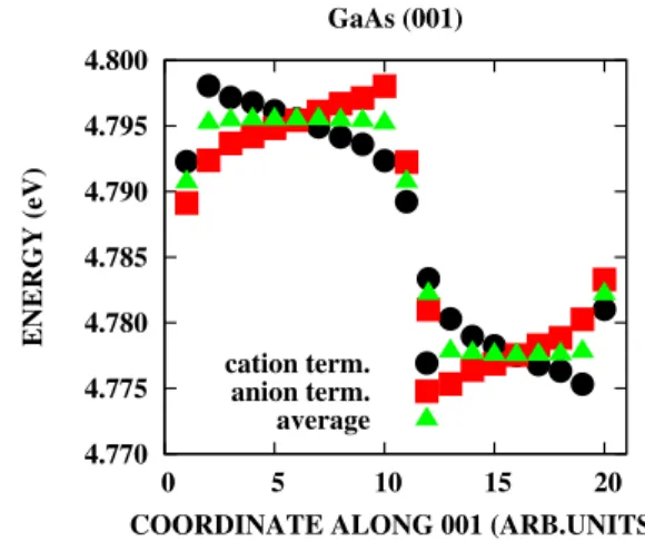
The supercell calculations are illustrated in Fig. 1 for GaAs subjected to tensile uniaxial strain. Figure1shows Eref
along the z-direction for the 共001兲 superlattice. The left side of the superlattice corresponds to the region exposed to
ten-a兲Electronic mail: ekadants@babylon.phy.nrc.ca.
4.770 4.775 4.780 4.785 4.790 4.795 4.800 0 5 10 15 20 ENER G Y (eV )
COORDINATE ALONG 001 (ARB.UNITS) GaAs (001)
cation term. anion term. average
FIG. 1. 共Color online兲 Superlattice calculation of the core ADP in GaAs. The energy reference is arbitrary. The共001兲 superlattice is subjected to 1% uniaxial tensile strain. The “strained part” of the supercell is on the left. The calculations have to be performed for anion- and cation-terminated super-lattices and the effects of the built-in electric field are averaged out.
APPLIED PHYSICS LETTERS 98, 023108共2011兲
0003-6951/2011/98共2兲/023108/3/$30.00 98, 023108-1 © 2011 American Institute of Physics
sile uniaxial strain. Note that Erefis larger in the strained part
of the superlattice which corresponds to positive deformation potential.
The absolute volume deformation potential for band␣at volume V is defined as aV
␣
= dE␣/dln共V兲, where E␣ is the
“absolute” band energy. We calculate ADPs for VBM as aVVBM= aV VBM/1s + aV 1s , where aV VBMax/1s
is the deformation po-tential with respect to Erefand aV
1s
was determined from the supercell calculations. The ADP of the conduction band minimum 共CBM兲 is given by aV CBM = aV VBM +共aV CBM − aV VBM兲, where共aVCBM
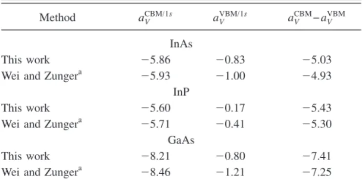
− aVVBM兲 is a well-defined deformation potential of the gap. The results of our calculations and results from Refs.8and5are summarized in TablesIandII. We find that all the ADPs for VBM of InAs, InP, and GaAs are positive. The existing ab initio models of biaxial strain12,13 were obtained assuming zero ADP of the core reference levels. Therefore, there is a need to develop a revised model for the biaxial strain. The共001兲 biaxial strain can be presented as a linear combination of hydrostatic and共001兲 uniaxial strains. The movement of Erefwith respect to some “absolute
refer-ence point” under the 共001兲 biaxial strain is described by dEref=关共1 + 储兲3− 1兴aV
1s
+共⬜− 储兲aV
1s/001
, where 储 and ⬜are
the in-plane and out-of-plane strain tensor elements and the first and second terms in dErefstem from the hydrostatic and
共001兲 uniaxial strains, respectively. TABLE I. Deformation potentials共eV兲 aV
VBM/1s
of VBM with respect to 1s core levels and the deformation potentials of the direct band gap aV
CBM − aV
VBM
for InAs, InP, and GaAs.
Method aV CBM/1s a V VBM/1s a V CBM− a V VBM InAs This work ⫺5.86 ⫺0.83 ⫺5.03
Wei and Zungera ⫺5.93 ⫺1.00 ⫺4.93
InP
This work ⫺5.60 ⫺0.17 ⫺5.43
Wei and Zungera ⫺5.71 ⫺0.41 ⫺5.30
GaAs
This work ⫺8.21 ⫺0.80 ⫺7.41
Wei and Zungera ⫺8.46 ⫺1.21 ⫺7.25
a
Linearized augmented plane wave共LAPW兲 calculation from Ref.7.
TABLE II. ADPs共eV兲 for conduction band minimum aV
CBM
, valence band maximum aV
VBM, and the deformation potentials of the direct band gap
aV
CBM− a
V
VBMfor InAs, InP, and GaAs.
Method aV CBM aV VBM aV CBM − aV VBM InAs This work ⫺4.31 0.72 ⫺5.03 Van de Wallea ⫺5.08 1.00 ⫺6.08 Li et al.b ⫺3.87 1.79 ⫺5.66 InP This work ⫺4.45 0.98 ⫺5.43 Van de Wallea ⫺5.04 1.27 ⫺6.31 Li et al.b ⫺4.10 1.83 ⫺5.93 GaAs This work ⫺6.24 1.17 ⫺7.41 Van de Wallea ⫺7.17 1.16 ⫺8.33 Li et al.b ⫺5.91 2.24 ⫺8.15 a
“Model solid” theory of Ref.5. b
LAPW calculations of Ref.8.
TABLE III. Coefficients obtained from the fit of biaxial strain-modified band edges to third degree polynomial in 储.
Band␣ C1 C2 C3 InAs CBM ⫺3554.24 203.81 97970.7 HH ⫺2653.54 12080 ⫺79225.8 LH 3831.07 74578.3 32446.9 SO 1202.52 ⫺83656.8 ⫺46808.1 InP CBM ⫺3447.64 925.234 62295.4 HH ⫺2122.07 11680.7 ⫺30662.1 LH 3806.34 107858 ⫺676415 SO 1993.34 ⫺119070 693622 GaAs CBM ⫺7345.78 ⫺501.231 163604 HH ⫺2117.63 20146 ⫺65765.3 LH 4357.87 52925.9 ⫺287271 SO 2370.2 ⫺52556 301211
FIG. 2. 共Color online兲 The 共001兲 BBEs as a function of the “in-plane” strain 储. The solid lines are fit to the polynomial of third degree in 储.
023108-2 E. S. Kadantsev and P. Hawrylak Appl. Phys. Lett. 98, 023108 共2011兲
The biaxial strain-modified band edges 共BBEs兲 which include the effects of the “relaxation” of the core levels are illustrated in Fig. 2 for InAs, InP, and GaAs, respectively. The ab initio BBEs for band␣are fitted to the polynomial of third degree EBIAXIAL
␣ = C1␣储+ C2␣储 2 + C3␣储 3 . The expansion coefficients are summarized in TableIII. The nonzero posi-tive ADPs of the core levels affect the evolution of band edges under biaxial strain by moving all bands up or down in energy. This shift depends on the magnitude of strain. For example, in the case of InAs subjected to the compressive biaxial strain共储⬍0兲, a situation encountered for InAs
quan-tum dot grown on GaAs substrate, the position of the refer-ence level Eref with respect to the “absolute energy
refer-ence” shifts down due to the overall negative change in the volume. For InAs subjected to compressive strain, the shift is illustrated in Fig. 3 for two values of natural band offsets 共210 and 460 meV兲. For a given value of the natural band
offset, the strained band offset is lower in the model which explicitly takes into account the finite ADP of the reference core levels. The strained band offsets can be thought of as a depth of the quasiparticle confinement. Therefore, combina-tion of the “uncorrected” BBEs with large NBOs will result in the localization of holes that is too strong which will in-fluence the theoretical predictions with regard to 共multi兲ex-citon complexes.
E. S. Kadantsev thanks the NRC-NSERC-BDC Nano-technology initiative for financial support. The authors ac-knowledge discussions with M. Zielinski, A. Voznyy, M. Ko-rkusinski, D. Dalacu, and R. Williams.
1
P. Hawrylak and M. Korkusinski, Single Quantum Dots: Fundamentals,
Applications, and New Concepts, Topics in Applied Physics Vol. 90
共Springer, Berlin, 2003兲. 2
S. Frédérick, D. Dalacu, J. Lapointe, P. J. Poole, G. C. Aers, and R. L. Williams,Appl. Phys. Lett. 89, 091115共2006兲.
3
M. W. McCutcheon, G. W. Rieger, J. F. Young, D. Dalacu, P. J. Poole, and R. L. Williams,Appl. Phys. Lett. 95, 221102共2009兲.
4
C. G. Van de Walle and R. M. Martin,Phys. Rev. Lett. 62, 2028共1989兲. 5
C. G. Van de Walle,Phys. Rev. B 39, 1871共1989兲. 6
A. Janotti and C. G. Van de Walle,Phys. Rev. B 75, 121201共2007兲. 7
S.-H. Wei and A. Zunger,Phys. Rev. B 60, 5404共1999兲. 8
Y.-H. Li, X. G. Gong, and S.-H. Wei,Phys. Rev. B 73, 245206共2006兲. 9
A. Baldereschi, S. Baroni, and R. Resta,Phys. Rev. Lett.61, 734共1988兲. 10
S.-H. Wei and A. Zunger,Appl. Phys. Lett. 72, 2011共1998兲. 11
Y.-H. Li, A. Walsh, S. Chen, W.-J. Yin, J.-H. Yang, J. Li, J. L. F. Da Silva, X. G. Gong, and S.-H. Wei,Appl. Phys. Lett. 94, 212109共2009兲. 12
P. R. C. Kent, G. L. W. Hart, and A. Zunger,Appl. Phys. Lett. 81, 4377
共2002兲. 13
E. S. Kadantsev, M. Zielinski, M. Korkusinski, and P. Hawrylak,J. Appl.
Phys. 107, 104315共2010兲.
14
P. Hohenberg and W. Kohn,Phys. Rev. 136, B864共1964兲. 15
W. Kohn and L. J. Sham,Phys. Rev. 140, A1133共1965兲. 16
U. von Barth and L. Hedin,J. Phys. C 5, 1629共1972兲. 17
L. Kleinman,Phys. Rev. B 24, 7412共1981兲. 18
J. P. Perdew and Y. Wang,Phys. Rev. B 45, 13244共1992兲. 19
E. Sjöstedt, L. Nordström, and D. J. Singh,Solid State Commun. 114, 15
共2000兲. 20
G. K. H. Madsen, P. Blaha, K. Schwarz, E. Sjöstedt, and L. Nordström,
Phys. Rev. B 64, 195134共2001兲. 21 http://exciting.sourceforge.net; version 0.9.151. 0.0 100.0 200.0 300.0 400.0 500.0 600.0 700.0 800.0 5.65 5.7 5.75 5.8 5.85 5.9 5.95 6 6.05 STRA INED BAND OFF SET [m e V ]
LATTICE CONSTANT [Å]
a1score=0 NBO=210meV a1score>0 NBO=210meV a1score=0 NBO=460meV a1score>0 NBO=460meV
FIG. 3. 共Color online兲 Energy of InAs VBM as a function of compressive biaxial strain EBIAXIAL
VBM = NBO+ C
1VBM储+ C2VBM储
2+ C 3VBM储
3for two differ-ence choices.
023108-3 E. S. Kadantsev and P. Hawrylak Appl. Phys. Lett. 98, 023108 共2011兲