HAL Id: in2p3-00118873
http://hal.in2p3.fr/in2p3-00118873
Submitted on 6 Dec 2006
HAL is a multi-disciplinary open access
archive for the deposit and dissemination of
sci-entific research documents, whether they are
pub-lished or not. The documents may come from
teaching and research institutions in France or
abroad, or from public or private research centers.
L’archive ouverte pluridisciplinaire HAL, est
destinée au dépôt et à la diffusion de documents
scientifiques de niveau recherche, publiés ou non,
émanant des établissements d’enseignement et de
recherche français ou étrangers, des laboratoires
publics ou privés.
Level 0 trigger decision unit for the LHCb experiment
J. Laubser, Hervé Chanal, R. Cornat, O. Deschamps, M. Magne, Pascal Perret
To cite this version:
J. Laubser, Hervé Chanal, R. Cornat, O. Deschamps, M. Magne, et al.. Level 0 trigger decision unit
for the LHCb experiment. 12th Workshop on Electronics for LHC and Future Experiments, Sep 2006,
Valencia, Spain. 297-301 p. �in2p3-00118873�
Level 0 trigger decision unit for the LHCb experiment
J. Laubser, H. Chanal, R. Cornat, O. Deschamps, M. Magne, P. Perret
for the LHCb Collaboration
Laboratoire de Physique Corpusculaire (IN2P3/CNRS), Clermont-Ferrand, France
[email protected]
Abstract
The Level-0 Decision Unit (L0DU) is the central part of the first trigger level of the LHCb detector. The L0DU receives infor-mation from the Calorimeter, Muon and Pile-Up sub-triggers, with fixed latencies, at 40 MHz via 24 high speed optical fiber links running at 1.6 Gb/s. The L0DU performs simple physics algorithm to compute the decision in order to reduce the data flow down to 1 MHz for the next trigger level and a L0Block is constructed. The processing is implemented in FPGA using a 40 MHz synchronous pipelined architecture. The algorithm can be easily configured with the Experiment Control System (ECS) without FPGA reprogramming. The L0DU is a 16 layer custom board.
I. T
HEU
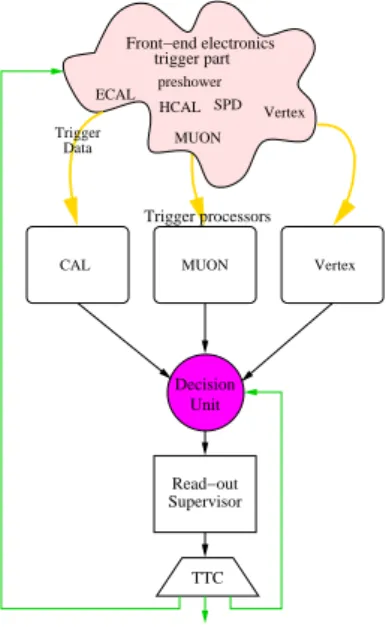
NITThe purpose of the Level-0 Decision Unit (L0DU) [1] is to compute the L0 trigger decision by using the information from the L0 sub-triggers in order to reduce the data flow from 40 MHz down to 1 MHz for the next trigger level [2] (see Figure 1).
ECAL MUON Vertex Trigger processors TTC MUON Vertex Front−end electronics SPD preshower Read−out Supervisor Decision Unit trigger part Trigger Data HCAL CAL
Figure 1: Simplified L0 trigger system
For that purpose, the L0 Decision Unit receives an event summary from the L0 calorimeter selection board [3], the L0 Muon trigger processor [4] and the L0 Pileup system, each with its own latency, at 40 MHz (see Figure 1). Then, a physics algo-rithm is applied to select events and delivers the L0DU trigger
decision to the Readout Supervisor (ODIN) [5] which takes the ultimate decision to accept or not the event. The L0DU trigger decision is encoded in a 16 bit explanation word (RSDA) [6]. At each event, a ”L0-Block data” is constructed and sent to the High Level Trigger (HLT) when the L0DU has received a L0Accept signal coming from ODIN via the Timing and Trigger Control system (TTC) [7].
The L0DU architecture is designed to be flexible in order to have the possibility to configure different algorithms through the Experiment Control System (ECS) [8] with the same pro-grammed architecture. Special triggers can be implemented with specific arithmetic and logical computations. Downscaling (accepted rate of a trigger channel) of the L0 trigger decisions and changing conditions of the decision (algorithm, threshold, downscaling factors, ...) are possible. Monitoring of perfor-mance and statistic analyses will be done by the hardware and the software. The motive of the decision is coded in an expla-nation word (L0DUrpt) in the L0Block data and is sent to the Data Acquisition (DAQ).
Special care of the good running and debugging of this unit is taken. Thus, in addition to an internal test bench based on RAM, a dedicated test bench has been developped [9]. It is based on an optical pattern generator board able to send test pattern during 18 LHC cycles.
Table 1: L0DU port summary
External system I/O # bits
CALO I 224@40MHz MUON I 256@40MHz PILE-UP I 64@40MHz Spare I 224@40MHz RSDA O 16@40MHz HLT O 1024@1MHz ECS IO
-PC Interface via USB IO
-A. Input and output data
The input data [10] are made up of several ”candidates” that correspond to the few highest transverse energy or momentum (Et, Pt) detected particles. Thus, the calorimeter sends one elec-tron, one photon, one neutral pion, one global neutral pion and the highest hadron as candidates. The muon detector sends the two highest muons for each quarter of the detector, while the vertex detector transmit the global condition in order to make a veto (no trigger allowed in case of multiple collision) calcula-tion. In addition, the total energy deposited in the calorimeter
and the SPD detector occupancy are also received by the L0DU. The data are sent on 32 bits words including a bunch identifi-cation number allowing to time align the incoming data since each has its own latency.
A total of 864 bits (Table 1) at a frequency of 40 MHz is ex-pected at input of the L0DU. The total latency of the L0 trigger is 4 µs and the L0DU latency budget is 500 ns counted from the late arriving sub-trigger data.
The L0DU transmits the decision within a 16 bits word at 40 MHz to trigger distribution system ODIN. This word contains the decision, a bunch crossing identification number. An addi-tional bit is used to ask for forced trigger for debugging and slow control purpose. Another bit allows timing tuning functions of the trigger distribution system. It is set when a given pattern of decision is detected over 5 events (the current event and the two events before and after): isolated decision or collision. The last bit is used as a status bit, and indicates to ODIN that the L0DU decision could be erroneous.
B. Architecture
For each data source, a ”Partial Data Processing” (PDP) system performs a specific part of the algorithm. It re-phases the data with the system clock, does the data time alignment and prepares the algorithm data. In this first step, the pipeline architecture is optimized for each L0 sub-trigger data and imple-ments pre-processing like searching the three highest Pt muon. Then, a ”Trigger Definition Unit” (TDU) processes the infor-mation to form a set of trigger conditions which are combined to compute the L0DU decision (see Figure 2).
Every trigger conditions are ORed to obtain the L0DU deci-sion after indivudal downscaling if needed.
Then, the decision word (16 bits) is sent to ODIN.
CALO MUON PileUp Spare
Partial Data Processing
Trigger Definition Unit
Decision word computation
Control Interface L0Block buider Decision word 16 bits @ 40 MHz DAQ 1024 bits @ 1 MHz PC ECS
Figure 2: L0DU logical architecture
The L0Block builder part constructs the L0Block. The
L0Block contains up to 32 words of 32 bits of data concerning an event (header, raw input data, processing algorithm partial results, etc. . .). It is sent to the DAQ system only when the ex-periment L0 trigger is received on the decision unit. For that, the L0Block is built for each event and stored into memories wait-ing for the L0 trigger and finally put into a FIFO when validated. Each validated L0Block is sent word by word at a 40 MHz. The control interface exploits signals delivered by the ECS to manage the algorithm parameters, the data processing algorithm behaviour, reset scenarios, slow control, on line debugging and monitoring and many other tasks like FPGA programming.
C. I/O format
All the L0 sub-triggers transmit their data via high speed optical links running at 1.6 Gb/s, 17 single optical fibers are expected from the L0 sub-triggers and 7 spare optical links have been added. This 17 single optical fibers are connected to 2 patch panels. Each patch panel converts the 12 single optical channels into a MPO fiber ribbon which is connected to the L0DU.
The L0DU implements two optical transceiver HFBR-782BE from Agilent, each connected to a ribbon. Then, 24 TLK2501 from Texas Instrument are used to deserialize the data. A data word is seen as two words of 16-bits at 80 MHz on the reception side.
The decision word is sent to ODIN over a point-to-point 16-bit LVDS link using a 3M pack connector (34-pins) and a twisted pair ribbon cable with 17 pairs.
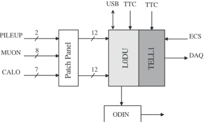
D. L0DU setup
The L0DU decision unit is implemented as a plug-in module on a standard LHCb DAQ board (TELL1) [11], (see Figure 3). The main data flow does not use the TELL1 board which con-sists in sending at 40 MHz the decision word to ODIN. The L0DU uses the TELL1 board for DAQ interface, for the ECS access through the CC-PC of the TELL1, for the power supply and the JTAG chain access through the CC-PC.
TELL1 L0DU USB TTC PILEUP MUON CALO 2 8 7 DAQ TTC ECS ODIN Patch Panel 12 12
E. Flexibility
For the design, an emphasis is put on flexibility. The use of FPGA makes this point easy to implement. As the data processing algorithm remains quite simple, most of the proba-bly needed functionalities can be implemented and then selected by the way of configuration register, without the need of a dedi-cated complex configuration software.
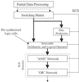
The L0DU architecture is flexible (see Figure 4), and allows to compute and to realize the most current types of algorithms. The structure of the flexible architecture is composed by a first step which is dedicated to the selection of all the inputs of the algorithm coming from the Partial Data Processing (PDP). This function is equivalent to an interconnexion switch. In a second step, the elementary conditions are elaborated by using arith-metic and logical operators. Then, a Programmable Logic De-vice (PLD) architecture is used to make combinaison, compose the triggers channels and take the decision.
Switching Matrix Partial Data Processing
Data Production
Selectable Arithmetic and Logical Operator
"AND" Network "OR" Network ECS PLD Structure Pre-synthezized logic cells
Figure 4: Flexible architecture
The interconnexion matrix is composed by multiplexors which allow to affect each output by a trigger data coming from the PDP. The elementary condition block is composed by macro-cells and allows to select the logical operators. The PLD structure allows to combine the elemenary conditions in a con-figurable way.
The architecture is not specific to a particular algorithm and is fully configurable without re-programming the FPGA. The structure and the way to compose step by step the algorithm introduce flexibility: new trigger channels can be added easily. Evolution are possible because unforeseen functionnalities can be added with no modification of the global architecture but will need a re-programmation of the FPGA.
The limits are imposed by the amount of pre-synthezized
macro-cells, the size of the interconnexion switch, the size of the PLD and the amount of logic elements available in the FPGA.
II. F
UNCTIONNALITIESThe L0DU is based on very simple algorithms combining some cuts on energy or impulsion of the candidates. Of course the type of selected physic events is conditionned by the applied algorithm. As an example, calorimeter candidates is selected by applying threshold on Et can be used to select b events while total Et can allow to reject multiple interactions.
Some more complex tasks are implemented: data synchro-nisation, time alignment, search for the 3 highest muons over the 8 candidates, sum of the two highest Pt muon, production of new data or combinaition between simple conditions to produce fine triggers.
Others functionnalities are implemented which do not con-cern directly the decision algorithm. The L0DU implements monitoring for on-line analysis like error counter, time align-ment checking, counter associated to the trigger channel and the L0DU decision.
The L0DU implements specific module for the commission-ing of the L0DU unit and the interface to the L0 sub-triggers, ODIN, the DAQ through TELL1 and check the behavior of the L0DU in a stand alone test mode.
III. L0DU T
ESTB
ENCHThe test of the L0DU and the test bench are more com-plex than the unit itself. A Specific pattern injection (GPL) has been developed to be able to emulate the L0 sub-triggers and to characterize the links used. This board allows to emulate physics run and failure like loss of synchronisation of the optical link or erroneous data.
A. GPL functional description
The GPL board allows to send test pattern on 24 optical fiber running at 1.6 GB/s. The pattern could be either a fixed pattern, a counter or a RAM content. The board is also able to acquire the L0 decision word sending at 40 MHz. The GPL registers and GPL RAM can be accessed with an USB interface or an ECS access through the L0DU plugged on the TELL1 board.
The GPL is compatible with TTC for synchronisation and with the standard LHCb crate and can be installed in the pit.
B. GPL board design
The GPL board (see Figure 5) relies on three Stratix FPGA, two are used for the processing and one is used for the control of the board. The GPL implements 12 external memories able to strore test pattern during 18 LHC cycle, a clock network and two optical channels. The GPL board has an emulated ODIN input and an USB interface for the control of the board. Special
cares have been taken concerning the clock network, the jitter filtering and the board place and route.
TTC Mezzanine Clock Network 12 Serializers TLK2501 Optical Transceiver 12 Processing FPGA RAMs L.A 12 Serializers TLK2501 Optical Transceiver 12 Processing FPGA RAMs L.A Processing FPGA L.A ODIN Input USB
Figure 5: GPL board design
C. Embedded test bench
A simplified version of this external test bench is imple-mented on the L0DU. It allows to test the behaviour of the L0DU architecture after installation by injecting known patterns with internal memories (Depth:256, Width:32). The processing results are stored and compared to the expected results. The comparison can be done either by the hardware either by the L0DU software. The internal test bench is composed by 24 RAM to store the test pattern, 2 RAM (Depth:256, Width:16) to store the results and the expected results. Nevertheless, the full debugging and the maintenance will be performed with the external test bench at laboratory.
IV. L0DU
BOARDA first prototype [1] has been assembled and tested at the begining of the year 2002. It was a simplified version that had neither ECS nor Timing Trigger Control connection and had a reduced number of inputs and outputs. The inputs and outputs were in LVDS format at 40 MHz via Ethernet CAT 5+ cables and RJ45 connectors.
Due the number of interconnexion between the L0 sub-triggers and the L0DU, it has been decided to use optical links. Furthermore, it has been decided to implement the L0DU as a TELL1 mezzanine in order to benefit of the ECS and DAQ paths. A new prototype has been designed, and all the function-nalities required for the L0DU are now implemented [12].
A. Design
The processing of the L0DU is done by two Stratix FPGA in BGA package due the hight number of interconnexion between the optical design part of the L0DU. Each, FPGA receives the data output bus of 12 TLK2501 deserializers. One of the
two procesing FPGA centralizes the information coming from the L0 sub-triggers and it is that FPGA which implements the definition of the L0DU algorithm. A dedicated FPGA is imple-mented on the L0DU to control de board. This control FPGA is connected to the TTC mezzanine, the ECS of the CC-PC of the TELL1, a USB interface and the processing FPGA in order to deliver the signals and the ECS.
TTC Mezzanine Clock Network 12 Deserializers TLK2501 Optical Transceiver 12 Processing FPGA 12 Deserializers TLK2501 Optical Transceiver 12 Processing FPGA Control FPGA ODIN Output RAM Quartz 80 MHz USB
RAM L.A L.A RAM L.A
DAQ Output
ECS
Figure 6: L0DU board design
The FPGA used for the processing are Stratix EP1S25-F1025-C7 in BGA package, and the control FPGA is a Stratix EP1S10-F780-C7 in BGA package.
B. L0DU processing
The first part of the internal design of the processing FPGA is composed by an optical module that allows to re-synchronise the data to the local system clock and converts for each optical link the input data flow 16 bits at 80 MHz into 32 bits at 40 MHz. This function implements errors synchronisation detec-tion and the demultiplexing data.
Then, a specific step is dedicated to the latency compensa-tion and time alignment between the different sub-trigger data. Data production, data formating and internal patch panel are introduced to prepare and to select the data that will be used in the Trigger Definition Unit.
Thresholds are applied on data to constitute the elementary condition that will be used in algorithm. Each elementary con-dition are combined, by a AND network, to form the trigger channel that are after downscaled. The decision of the L0DU is taken by apllying a OR network between the downscaled trigger chanel.
C. ECS and Software
The actual prototype allows to access to the L0DU through the I2C bus of the CC-PC [8] of the TELL1 board. A software
control system for L0DU is being designed to be integrated in the LHCb software environment. According to the LHCb rules, the software interface in based on the PVSS [13] and use the JCOP [14] control framework for the integration of the hard-ware.
D. Test and results
All the interface and the functionnalities of the L0DU have been tested and validated: DAQ interface, ECS and JTAG ac-cess, ODIN link and all the optical links. The Bit Error Rate (BER) of each optical link has been qualify and is below 10−12
as required for the LHCb experiment [15]. The ODIN link has been qualified with a BER below 10−12.
Various types of algorithm have been implemented and tested on the board with realistic data generated from a sample of simulated physics event. This prototype is closed to the final version and allows to evaluate the ressources and the limation of the board.
E. Final version of the L0DU
The limation of the actual design is due to the logical ressources of the FPGA. The upgrade for the final version is to implement FPGA with more logic ressources with the same package, to add interconnexion between the two processing FPGA and add spare connexion with the TELL1 board.
V. C
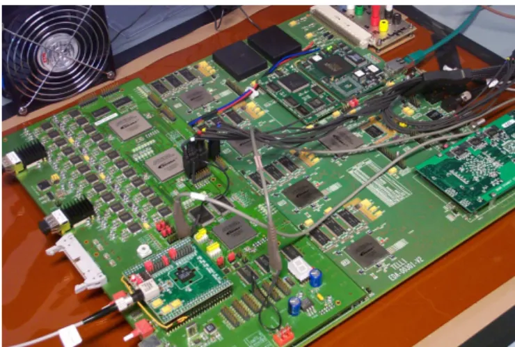
ONCLUSIONThe figure 7 shows the second prototype of the L0 Decision Unit plugged on the TELL1 board. The L0DU board is com-plex due to the high density of signals and the high frequency of signals. Many Specctra Quest simulations must have been done before manufacturing and allowed to make a such design without hardware failure. This prototype will be used during the LHCb detector commissioning phase.
Figure 7: L0DU board plugged on a TELL1
R
EFERENCES[1] R. Cornat, J. Lecoq, P. Perret, Level 0 Decision Unit for LHCb, LHCb 2003-065, 2003.
[2] TDR Trigger system.
[3] U. Marconi et al., The selection board, EDMS 749121.
[4] J. Cachemiche, R. Legac, Specification of the Muon trig-ger processor.
[5] R. Jacobson, Readout Supervisor design specification, LHCb 2001-012.
[6] R. Jacobson, Specification of the L0DU-ODIN link, EDMS 478756, 2004.
[7] http://ttc-web.cern.ch/TTC/intro.html.
[8] http://lhcb-online.cern.ch/lhcb-online/ecs/default.html.
[9] H. Chanal, M. Magne, J. Laubser, P. Perret et al., Specifi-cation of the GPL board, 2006.
[10] J. Laubser, M. Magne, P. Perret et al., Specification of the L0DU trigger input and output, EDMS 528259, 2006.
[11] G. Haefeli et al., TELL1 specifiation, EDMS 487730.
[12] J. Laubser, H. Chanal, M. Magne, P. Perret et al., Specifi-cation of the L0DU unit, 2006.
[13] http://itcobe.web.cern.ch.itcode/Services/Pvss/welcome.html.
[14] Architecture working group, Frame work design proposal, CERN-JCOP 2000-007, 2001.
[15] M. Muecke, V. Bobillier, J. Christiansen et al., Qualifi-cation of the optical links for the data readout in LHCb, EDMS 680438, 2006.