Design for Manufacturability with Regular
Fabrics in Digital Integrated Circuits
By
Mehdi Gazor
B.S., Electrical Engineering and Computer Science University of California at Berkeley, 2003
Submitted to the Department of Electrical Engineering and Computer Science in partial fulfillment of the requirements for the degree of
Masters of Science in Electrical Engineering and Computer Science at the
MASSACHUSETTS INSTITUTE OF TECHNOLOGY
May 11, 2005
@ Massachusetts Institute of Technology, 2005. All Rights Reserved.
Author __
Electrical Engineering and Computer Science May 11, 2005
Certified by
-Nj
Duane S. Boning
Professor of Electrical Engineering and Computer Science Thesis Supervisor
Accepted by Arthur C. Smith
Chairman, Department Committee on Graduate Studies Electrical Engineering and Computer Science
MASSACHUSETTS NSTITTE OFTECHNOLOGY
Design for Manufacturability with Regular Fabrics
in Digital Integrated Circuits
By
Mehdi Gazor
Submitted to the Department of Electrical Engineering and Computer Science on May 11, 2005 in Partial Fulfillment of the Requirements for the Degree of Master of Science in
Electrical Engineering and Computer Science
Abstract
Integrated circuit design is limited by manufacturability. As devices scale down, sensitivity to process variation increases dramatically, making design for manufacturability a critical concern. Designers must identify the designs that generate the least systematic process variation, e.g., from pattern dependent effects, but must also build circuits that are robust to the remaining process or environmental random variations. This research addresses both ideas, by examining integrated circuit design styles and aspects that can help curb process variation and improve manufacturability and performance in future technology generations.
One suggested method to reduce variation sensitivity in system designs has been the concept of design regularity. Long used in FPGAs, and SRAMs, the concept of repeatable blocks is examined in this work as a method of reducing circuit variation. Layout based variation is examined in three designs with different distinctions of
regularity: a Via-Patterned Gate Array (VPGA) FPU, a Berkeley BEE-generated decoder, and a low power FPGA. The circuit level impact on variation is also considered, by examining several circuit architectures. This includes analysis of the novel Limited Switch Dynamic Logic (LSDL) style, which reduces design area and encourages regularity through minimum logic sizing. Robustness to spatial variation and slanted plane effects is examined with a common-centroid based layout methodology for digital integrated circuits. Finally, a methodology is introduced in the form of the Monte Carlo Variation Analysis Engine whereby distributed process variables are fed into repeated simulation runs, output metrics are recorded, and regressions are measured to expose design sensitivities. The results for different layout and circuit design styles identify improvements that may be made to improve robustness to variation. We show that design regularity is a significant factor in mitigating sensitivity to process variation and is worthy of further examination.
Thesis Supervisor: Duane S. Boning
Acknowledgements
I would not be where I am today without the love and hard work of my parents, so first and foremost I wish to thank them for all I have today. The same can be said for my sister, grandparents, and extended family, all of whom have given me tremendous support and encouragement throughout the years.
The past two years at MIT have been tremendously rewarding for me, both academically and extracurricularly. I have been fortunate enough to learn from the best engineers and scientists in the world and will forever look upon the experience as truly enlightening. I would like to thank my research advisor, Duane Boning, for being the most humble, flexible, and supportive advisor I possibly could have asked for. He entrusted me with the creative freedom early on to explore research ideas, for which I am grateful. These years at MIT would not have been the same without my close friends, Nir Matalon and Kenny Kamrin, or my wonderful office mates over my time, Karen Mercedes Gonzilez Valentin Gettings, Tyrone Hill, Kwaku Abrokwah, Hayden Taylor, Hong Cai, Shawn Staker, Xiaolin Xie, Karthik Balakrishnan, and Daihyun Lim.
On the research end, I would like to thank the DARPA/MARCO Center for Circuits, Systems, and Solutions (C2S2) for sponsoring my research. I would like to thank Larry Pileggi and Veerbhan Kheterpal of CMU for their early guidance for my research with their VPGA technology. I would like to thank Sani Nassif of IBM Austin Research Lab, for introducing me to LSDL and giving me the opportunity to present my research at ARL. I would like to thank Brian Richards and Bora Nikolic of UC Berkeley, for giving me access to their BEE-generated decoder design for preliminary analysis. I would like to thank Hong Cai right here in the Boning group, for simulating CMP, ECD,
and other profiles with his models for the designs I researched. I would like to thank Frank Honore (MIT), Anantha Chandrakasan (MIT), and Peter Holloway (National Semiconductor), for granting me use of Frank's low-power FPGA design for layout analysis. Finally, I would also like to thank Aaron Gower-Hall and the entire Praesagus team for creating user friendly extraction tools and giving our group the privilege to use them. These models have helped me tremendously for my research.
Table of Contents
Abstract ... 2 Acknowledgem ents ... 5 Table of Contents ... 7 Table of Figures ... 9 Chapter 1 Introduction and Background ... 111.1 The Current Status of Integrated Circuits ... 11
1.2 Sources and M odels of Process Variation ... 12
1.3 D esign For M anufacturability ... 14
1.4 Sum m ary and D irections ... 20
Chapter 2 Manufacturability of Regular Fabrics and Flows ... 23
2.1 M otivation for Regularity ... 23
2.2 Via-Patterned Gate Arrays: A Regular Fabric ... 27
2.3 Berkeley Emulation Engine (BEE): A Semi-Regular Flow ... 32
2.4 M IT Low Power FPGA ... 35
2.5 Results Sum m ary ... 38
Chapter 3 Exploring Regular Circuit Architectures ... 41
3.1 Limited Switch Dynamic Logic (LSDL) Architecture ... 41
3.2 Dom ino and Static Circuits ... 43
3.3 Adder D esign ... 44
3.4 Results Sum m ary ... 48
Chapter 4 Robustness Analysis Through Historical MOSIS Models ... 49
4.1 Historical Param etric M OSIS M odels ... 49
4.2 M O SIS-based robustness analysis ... 50
4.3 Results Sum m ary ... 54
Chapter 5 Analysis of Circuits Architectures for Process Variation-Induced Errors ... 55
5.1 Clock Jitter...56
5.2 Clock Skew ... 57
5.3 Clock Slew ... 59
5.4 Data Slew ... 61
5.6 Isolated Process Variable Analysis... 66
5.7 Layout-Based Variation Trends... 68
5.8 Results Sum m ary ... 71
Chapter 6 Monte Carlo-Based Variation Analysis Engine ... 73
6.1 M ethodology ... 73
6.2 M ism atch Variation ... 77
6.3 Chip-to-Chip Variation ... 79
6.4 Overall Variation ... 80
6.5 Sensitivity Regression Analysis of M onte Carlo Data ... 82
6.6 Adder Perform ance Com parisons ... 85
6.7 Correlation Analysis ... 87
6.8 Results Sum m ary ... 90
Chapter 7 Com m on Centroid-Based DFM ... 93
7.1 Com m on Centroid-Based Layout M ethodology ... 93
7.2 Experim ents with Regularity ... 96
7.3 Tests and Data ... 98
7.4 Results Sum m ary ... 107
Chapter 8 Conclusions and Future W ork ... 109
8.1 Conclusions...109
8.2 Future W ork ... 111
Table of Figures
Figure 1.1 Process variation types and sources [20] ... 13
Figure 1.2 Increasing geometrical primitives increases uncertainty in final
design [1] ... . . 16
Figure 1.3 Some layout-induced variation sources [3] ... 16
Figure 1.4.1 Copper plating problems due to irregular pattern density in design
[2] ... . 18
Figure 1.4.2 CMP dishing/erosion problems due to irregular pattern density in
design [2] ... . . 18
Figure 2.1 A large number of systematic or deterministic contributions (right)
to a parameter can appear in aggregate as a single "random"
distribution (left) [7] ... 24 Figure 2.2 Scope of variation in semiconductor manufacturing [6] ... 25
Figure 2.3 Shortcomings in optical lithography. Source: A.Strojwas & W.
M aly, C M U ... 26
Figure 2.4 Via-patterned gate array design and single logic block component.
Source: L .Pileggi ... 28
Figure 2.5 Normalized VPGA metal densities ... 29
Figure 2.6 Process for VPGA FPU metal 1 interconnect ... 30
Figure 2.7 Modeled copper thickness, oxide erosion, plated thickness, and
post-CMP copper thickness for VPGA FPU's metal 4 interconnect ... 31 Figure 2.8 Pattern density (with and without dummy fill) for BEE-generated
layout ... . 33
Figure 2.9 Copper dishing and oxide erosion (with and without dummy fill)
for BEE-generated layout ... 33
Figure 2.10 Plated thickness and post-CMP copper thickness (with and without
dummy fill) for BEE-generated layout ... 34
Figure 2.11 3D visualization of BEE-generated decoder, post-CMP ... 35
Figure 2.12 Pattern density (with and without dummy fill) for MIT FPGA. ... 36
Figure 2.13 Electrochemical deposition (ECD) copper damascene envelope
profile for MIT Honore/ Chandrakasan low power FPGA. ... 37
Figure 2.14 3D visualization of MIT Honore/Chandrakasan low power FPGA,
post-C M P ... 38
Figure 3.1 Domino vs. LSDL schematics ... 42
Figure 3.2 LSDL sizing vs. domino Sizing ... 43
Figure 3.3 Topology for 16-bit CLA adder design. Critical path is measured at
SU M 14 ... 45 Figure 3.4 Adder layouts, by circuit architecture ... 46
Figure 4.1 Maximum adder speeds and distributions under historical MOSIS
Figure 4.2 Average adder power at maximum speeds in historical MOSIS
process m odels ... 53
Figure 4.3 Leakage power in historical MOSIS process models ... 54
Figure 5.1 Figure 5.2 Figure 5.3 Figure 5.4 Figure 5.5 Figure 5.6 Figure 5.7 Figure 5.8 Figure 5.9 Figure 5.10 Figure 5.11 Figure 5.12 Figure 5.13 Figure Figure Figure Figure Figure Figure 6.1 6.2 6.3 6.4 6.5 6.6 Figure 6.7.1 Figure 6.7.2 Figure 6.8 Figure 6.9 Figure 6.10 Figure 7.1 Figure 7.2 Figure 7.3 Figure 7.4 Figure 7.5 Figure Figure Figure Figure Figure 7.6.1 7.6.2 7.7.1 7.7.2 7.7.3 C lock jitter [16] ... 56
Clock jitter comparisons for domino and LSDL adders ... 57
C lock skew [16] ... 58
Clock skew comparisons for domino and LSDL adders ... 59
Non-desirable clock slew ... 60
Clock slew comparisons for domino and LSDL adders ... 61
Data slew comparisons for domino, LSDL, and static adders ... 63
Slanted plane chip-scale effect and directional trends examined ... 64
Grid division of design for slanted plane performance simulation ... 65
Slanted plane effect analysis for 8 directional trends (strength into direction) ... 66
Impact of isolated process variable (110% of nominal value) on adder perform ance ... 67
Adder pattern density analysis ... 69
Polysilicon feature size binning ... 70
Flow chart for Monte Carlo variation analysis methodology ... 77
Mismatch Monte Carlo variation analysis for adder architectures ... 78
Chip-to-chip Monte Carlo variation analysis for adder architectures...80
Overall Monte Carlo variation analysis for adder architectures ... 81
Output measurements taken for Monte Carlo runs ... 83
Multiple regression sensitivity analysis for Monte Carlo adder sim ulations ... 84
Boxplots for adder output metrics ... 86
Boxplots for adder output metrics ... 87
Group plot matrix and correlation matrix for domino adder ... 88
Group plot matrix and correlation matrix for LSDL adder ... 89
Group plot matrix and correlation matrix for static adder ... 90
Suggested linear process variation gradient (slanted plane effect) ... 94
Centroid of weighted masses ... 95
Positioning of blocks affects centroid matching ... 96
Common centroid-based layout styles ... 98
Layout of very regular-class C inverter chain, with grouped cells and matching centroids among blocks ... 99
Boxplots for centroid-based layout style output metrics ... 100
Boxplots for centroid-based layout style output metrics ... 101
Sensitivity tests for centroid-based inverter chain layouts ... 104
Sensitivity tests for centroid-based inverter chain layouts ... 105
Chapter 1
Introduction and Background
Basic trends in integrated circuit manufacturing are discussed in this chapter, including the growing awareness of the impact of process variation. Models of variation that will be used throughout this work are introduced, as are suggested methods currently employed to help reduce some of the variation sources.
1.1
The Current Status of Integrated Circuits
As of this writing, integrated circuits are being manufactured in 90 nm technology and microprocessors can reach speeds of over 4 GHz. At these feature sizes and performance levels, process variation is a critical design consideration. Unfortunately, the process variation problem will only get much worse, given the predicted scaling that will occur in designs [21]. As technologies continue to scale, designers must consider constraining die size growth while continuing to scale supply and threshold voltage to overcome the predicted limiters in future technologies, namely power delivery and dissipation. Domino logic will continue to lose its performance advantage over static logic, subthreshold current will increase, and designs will become more susceptible to soft errors as supply and threshold voltages scale [12].
Models for 50 nm production of digital circuits have predicted that almost an entire generation of performance gain can be lost due to systematic within-die fluctiations
[23]. Therefore, designers are at a crossroads in time where design tolerances must
tighten against increasing process variations to sustain Moore's Law.
1.2
Sources and Models of Process Variation
Process variations have, to a great extent, dictated the style and progression of design in integrated circuits. Designers have attempted more robust designs and CAD engineers have developed more accurate methodologies to ensure that design performance after manufacturing matches that after simulation. Understanding the sources of process variations is critical to developing better design rules for circuits, ensuring accurate tests for robustness, and controlling manufacturing conditions for optimal design yield.
Process variations in integrated circuits can generally be classified into environmental and physical components. Environmental variations, or deviations in operating conditions arising during circuit execution, depend primarily on architectural and operating decisions, such as power grid design and component placement. Variations in power supply, switching activity, temperature, and ambient noise are all examples of environmental variations that can impact a design [20].
Physical variation, however, is also of great concern in integrated circuit design. Figure 1.1 illustrates the classifications of physical variations in design, classifying sources into device and interconnect branches and also into geometry, material, and electrical categories. This figure reminds us that variation is introduced at every stage in the build process of an integrated circuit. For instance, variation may affect layout geometries and induce unexpected coupling capacitances, may continue through manufacturing in the form of excess deposited oxide, lithography deviations and reduced
etch, and then finally through inductance from packaging materials. The possibilities are infinite, as one can imagine. Because the manufacturing process may never be deterministic, a designer's only hope is to curb the known sources of variation through design techniques and methodologies that are known to reduce process variation.
Process Variation Types and Sources
Environmental Physical
I
Devi( - power supply switching activity + temperature + noisee Geometry Interconnect Geometry
-Device Material Parameter Interconnect Material Parameter
Device Electrical Parameter line width and
contact and via line space film thickness doping threshold voltage resistance metal thickness
4-lateral dimension deposition discrete dopant metal resistivity+ dielectric thickness
-(ength, width) and anneal leakagecurrent dielectric constant+ contact and via
size+-Fig. 1.1. Process variation types and sources [20].
Lumped statistical models, used in this work, are the most basic approach to describing variation. Given any process variable P, the lumped statistical model assumes that P is the sum of some nominal value Po and a variation measure AP. The variation component is assumed to be a zero mean Gaussian random variable with variance up
[20].
P = PO + AP AP ~ N(0,p2)
(1.1) (1.2)
More accurately, we can characterize the variation components of a process variable into a greater number of more narrowly defined variables. Interdie and intradie
variation are two such ways to classify physical variation sources, as considered in Equation 1.3. Interdie variation is the difference in the value of some parameter across nominally identical die and is typically accounted for in circuit design as a shift in the mean of some parameter value equally across all devices or structures on any one chip. An interdie trend may be oxide thickness, for which variations across an entire wafer may be significant. Intradie variation is the deviation occurring spatially within any one die [20]. Mismatch variation, for example, is something that affects local dies.
P = PO + Pinterdie + Pintradie + AP (1.3)
Because of the small area of the die, intradie variation for any process variable is modeled as a linear function of position, with (ox and Wyy as the said components.
Interdie variation, however, is more complicated, as many contributions many factor into such a variable. Equations 1.4 and 1.5 detail these components. Interdie variation is treated as a zero mean Gaussian random variable with variance 1interdie2 [20].
Pintradie(X,Y) = W(w, x, y) = Wo + COxx + COy (1.4)
Pinterdie = P fab-to-fab + Plot-to-lotfab) + Pwaferto-wafer(lOt) + Pdie-to-die(wafer) (1.5)
Pinterdie ~ N(,interdie2) (1.6)
1.3
Design for Manufacturability
Through years of research and production, a few key rules have developed in the semiconductor industry, which make up the concept of Design for Manufacturability (DFM). This idea encourages providing better process/circuit design prior to manufacturing, to allow for faster yield learning, and stabilizing the manufacturing by
minimizing process variability. DFM can be accomplished through a combination of minimizing process variations, and minimizing device and circuit sensitivities to process variations. This can be accelerated once the process is statistically characterized, exposing inefficiencies [9]. Many of the rules advocated in the DFM method include measures to mitigate pattern dependent variation, such as reduction of geometric primitives, layout regularity, redundancy techniques, pattern density uniformity, and optimal process feature sizing. Other areas of consideration in DFM are design for robustness and design for test. These suggested approaches are detailed below and considered in this research.
Reduction of Geometric Primitives
A geometric primitive refers to the category of shape in a design. The rectangle is
the most basic primitive in circuit layout. With each new geometric primitive comes a new set of uncertainty in processing. Primitives process differently, whether in
lithography, etch, plating, or through other steps in the process cycle. Complicated Resolution Enhancement Techniques (RET), depicted in Figure 1.2, must be applied to compensate for the distortions that new primitives may introduce. These techniques are costly and often insufficient for arbitrary random layout patterns [5]. Reducing the number of these primitive shapes in a design ensures higher certainty during the manufacturing stages, and is an important component of design for manufacturability.
Mask Layout Predicted Silicon Layout
DESIGN MASK WITH OPC RESULT ON WAFER
Fig. 1.2. Increasing geometrical primitives increases
uncertainty in final design [1].
Layout Regularity
Design performance has been correlated with the methodology and technique used during transistor layout [3]. Figure 1.3 illustrates some of the layout techniques that may affect performance in a design. Number of fingers per transistor, transistor orientation, proximity spacing, local and global effect of polysilicon density, interconnect orientation, choice of metal layer, and coupling capacitance across metal layers are all factors that can be constantly monitored and corrected during the layout process. Consistency is an important factor in this stage of the design process, as is an understanding of the manufacturing impact of layout styles.
Polysilicon fingers
Low Poly High Poly Density Densirty
DUfferent Poly Density Different Line Spacing Orientation
Fig. 1.3. Some layout-induced variation sources [3].
Redundancy to Improve Manufacturability
To improve planarity of polysilicon or metal layers in a design, metal "dummy"
fill is inserted throughout each layer. Dummy fill consists of redundant pieces of metal
placed in empty areas of a design with automated CAD tools to increase planarity. At the cost of increased capacitance, this fill narrows the layer's range of pattern density and significantly reduces CMP variation. Inserting dummy cells and dummy transistors are also methods for reducing edge effects for transistors, memories, and other blocks in a design. Finally, redundant via placement may improve manufacturability by decreasing the likelihood that a single via causes logical failure in a design due to bad processing. Combined, these techniques are a wise combination to reduce the variation effects of manufacturing and improve overall yield in an IC process.
Pattern Density Uniformity
One of the more understood culprits of systematic process variability is the irregularity in surface topography due to an unevenly distributed pattern density [2]. In Figure 1.4.1, the high pattern density region on the left results in a plating bulge, whereas the low density region to the right creates plating recesses. The electroplating-induced topography variation interacts with additional pattern effects in chemical-mechanical polishing (CMP), as seen in Figure 1.4.2.
Bulge
Fig. 1.4.1. Copper plating problems due to irregular pattern density in design [2].
Field Oxide Loss
Dishim g E rosion
Fig. 1.4.2. CMP dishing/erosion problems due to irregular pattern density in design [2].
Fluctuations in local metal thickness can affect the resistance and capacitance of the region, adding unexpected loads to wires, for example. Clock skew resulting from mismatch in the affected interconnect is one important effect of non-uniform pattern density. Electromigration also becomes an increased concern with sub-optimal non-regular metal thicknesses [2]. In the worst case, logical failure ensues from the improper plating and polish of the design.
Fortunately, dummy fill algorithms have the ability to compensate for the non-uniformity of most designs. Though dummy fill can alleviate macro-level fluctuations in pattern density uniformity, it is not a complete solution. Dummy fill introduces significant capacitance to a design, which may be a high cost for high performance circuits. Therefore, a designer must still consider the most regular approach to design
Optimal Feature Sizing
Local feature size records the smallest width of features in a small area on a chip. Various sizes and interaction distances among local wires, transistors, and other design components create this feature size variation. The resulting non-uniformity may affect pattern density and may result in copper dishing or oxide erosion variation [2], as illustrated in Figure 1.4.2. Optimally, all areas of a design have uniform feature sizes, encouraging consistent processing across the chip. Well characterized feature sizes could remove some of the uncertainty present in the manufacturing process, and are therefore advocated in the DFM methodology.
Performance Robustness
A careful designer will examine the timing slack across his circuit, whether for
clock distribution or data arrival delays. More importantly, he or she will design with tolerances for error in mind. These include considerations for process variations, such as transistor mismatch and die-to-die variation, as well as for environment variables, such as power supply deviations. Design for robustness integrates these considerations with well constructed tests for performance under the worst process circumstances. The most robust designs, therefore, are the ones that can operate in light of these adverse conditions.
Design for Testing
Chip design complexity and run costs have forced designers to consider testability of design before fabrication. Design for test is now a critical part of the IC design
process, with much development going into the areas of test structures, scan chains for test, and on-chip measurement techniques [3]. Design for manufacturability intersects with design for test, together ensuring robustness to process errors and a clear understanding of these errors when they do occur.
1.4
Summary and Directions
Process variation has become an increasing concern in integrated circuit manufacturing. The many sources and classifications of variation were described, and a lumped statistical model for quantifying variation in design was introduced. Design for manufacturability (DFM) was presented as a school of thought for curbing integrated circuit process variation during the design stage. Many of the considerations advocated in DFM were introduced and described, with much of the focus on methods to reduce pattern dependent variation.
Going forward, there are two key variation reduction ideas throughout this work. One is that some designs and design styles generate less process variation, i.e. more regular layout actually creates less pattern dependent variation. The second idea is that different design styles are more or less robust to the remaining process or environmental random variations, whether systematic or random. This research addresses both ideas, by examining integrated circuit design styles and aspects that can help curb process variation and improve manufacturability and performance in future generations.
The ideas and methods described in this chapter will be used to examine the impact of regularity on reducing pattern dependent variation in digital integrated circuits. In Chapter 2, preliminary comparisons will be done on logical fabrics that advocate the
use of regularity against more traditional non-regular designs. Using the variation models presented in this chapter, this work develops and analyzes an assortment of tests for regular and non-regular circuit architectures in Chapters 3 through 5. A Monte Carlo
methodology and sensitivity analysis are later introduced in Chapter 6 as methods to measure and compare design vulnerability to variation. Finally, a novel way to measure and explore the impact of regularity on variation robustness based on layout placement is introduced and evaluated in Chapter 7.
Chapter 2
Manufacturability of Regular Fabrics and Flows
Several of the considerations introduced in the previous chapter for design for manufacturability can be addressed with the notion of regularity in design. This chapter explores the potential of using regular fabrics as a method to reduce pattern dependent variation in designs. Three designs are analyzed and compared. The regular via-patterned gate array (VPGA) is compared against more traditional ASIC and regular
FPGA designs to evaluate manufacturability potential. Each of these designs with and
without dummy fill is also evaluated to determine the effectiveness of dummy fill in reducing edge effects and pattern dependent variation.
2.1
Motivation for Regularity
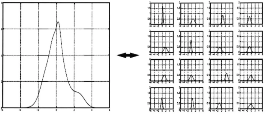
As designs become smaller and more intricate, the effects of process variation become more apparent and intolerable. These variations are either random or systematic, the latter of which occur in a reproducible fashion. A single systematic process variable may be the aggregate sum of numerous individual deterministic contributions, as visualized in Figure 2.1. Our goal is to identify these systematic variations and thus adopt layout and design approaches that both minimize these variations in the first place, and are robust to the remaining systematic or random variations.
4-4- 4
Fig. 2.1. A large number of systematic or deterministic
contributions (right) to a parameter can appear in aggregate as a single "random" distribution (left) [7].
To eliminate systematic variation would reduce much of the process variation that tends to occur during fabrication. Though there is no way to completely eliminate systematic variation, one proven way to reduce this type of variation has been through
well characterized devices. Once the manufacturability of these small structures is
understood and optimized, there is less likely to be systematic variation involved during the fabrication process. It then follows that larger structures built of these smaller units will also exhibit the manufacturability advantages of its smaller units, reducing the intradie variation component visualized in Figure 2.2. This is the core idea behind regularity and regular fabrics [5].
Regular fabrics are a general term for the digital architectures that exhibit these
modular, repeatable logical components. Traditional examples include the field
programmable gate array (FPGA) which uses repeated configurable logic blocks (CLBs) to create a powerful grid of programmable switches.
Regular structures have the manufacturability advantage over more custom ASICs due to their well-characterized, repeated components. In spite of a smaller die area,
custom designs tend to have lower yields and fewer working dies per wafer [4]. Once smaller pieces are modeled and well understood in terms of the effect of process variation, lithography, and etch, then the regular design that is composed of these smaller logic blocks can be well understood. This advantage has tremendous cost and yield implications, since reliability and robustness can improve over non-regular designs.
Lot-to-Lot
Wafer-lo-Wafer (or within Lot)
Within Wafer
EIEf000
:1J :3 Eomna LTd
Paramotior Intradie
Fig. 2.2. Scope of variation in semiconductor
manufacturing [6].
Feature level variation is a large concern in pattern sensitive processes such as lithography, plating, etch, and deposition. Layout printability challenges have become extremely severe due to: 1) high NA (numerical aperture), off-axis illumination schemes (angular, quadrupole, dipole) and small depth of focus; and 2) large mask error enhancement factor (MEEF). Moreover, etch and chemical mechanical polishing (CMP), which depend on intra-layer layout density variation, add to the challenges [5]. The
difficulty of lithography is compounded when the design is composed of an assortment of geometric primitives, orientations, and interaction distances, as suggested in Figure 2.3. It is increasingly difficult to print and pattern complex figures due to larger interaction distances. Resolution enhancement techniques (RETs), which predicatively correct for errors in lithography, are costly and insufficient for arbitrary layout patterns [5].
Sensitive to grow - Sensitive to
due to defocus Sensitive to shrink Sensitive to resist effects
due to defocus exposure varation
Fig. 2.3. Shortcomings in optical lithography. Source: A.
Strojwas & W. Maly, CMU
To reduce the problem complexity and achieve the desired performance and yield objectives, new solutions must explore more deeply the concept of regularity. The ultimate solution would be based on a full chip layout being assembled out of a set of patterns that are guaranteed to print for given lithography, etch and CMP process windows [5]. A regular fabric would ideally have a single logic block optimized for
these mentioned properties, reducing the uncertainty in lithography or later stages of fabrication. Regularity at the feature level and device level will be a great step in reducing spatial variation, thereby reducing systematic variation at the intra-die level.
Regular structures are critical in future scaled designs. W. Maly concludes that only by applying in a design highly geometrically regular structures, created out of the limited smallest possible number of unique geometrical patterns, can one hope to contain
the cost of nanometer ICs on the manageable level [11]. A regular architecture that employs many of the advocated regular structures is described and evaluated in the next
section.
2.2 Via-Patterned Gate Arrays: A Regular Fabric
The via-patterned gate array (VPGA) is a new digital architecture that takes traits from both custom ASIC and fully programmable architectures, like FPGAs [22]. Developed at Carnegie Mellon University, the basic idea behind these structures is to use repeatable logic units in a grid-like fashion, like FPGAs, to construct a larger operational unit. The first metal layers include the regular logic structures and the higher metal layers are composed of regular interconnect grids. A VPGA is "programmed" one time during fabrication through strategic placement of vias across the interconnect layer, to customize the logical operation of the design. In this respect, via-patterned gate arrays can be considered a regular, yet semi-custom ASIC. Its regular logic structure and the restriction of via placement to only a few metal layers not only decreases mask cost, but also has the potential to increase manufacturability tremendously.
Fig. 2.4. Via-patterned gate array design (left) and single logic block component (right). Source: L. Pileggi.
VPGA cells contain simpler elements such as nands, nots, muxes, and pass gates
and are highly optimized to be robust to process variations. Figure 2.4 depicts both a
VPGA design and an individual cell component, which consists of simple logic elements.
Used together, the cells form a regular fabric that is also tuned for successful fabrication. One major metric of a manufacturable design is the composition of its pattern density. In Figure 2.5, the range of interconnect pattern density across three metal layers can be visualized. In each individual layer, the range is no more than 5%, a number substantially lower than that of traditional ASIC layouts. This uniformity in interconnect density will ensure that many systematic variations during fabrication will be kept close to minimal, improving manufacturability.
0.45 0 0.45 0.1 0.4 0.1 0.4 0.2 0.35 0.2 0.35 0.3 0.3 0.3 .4 0.25 0 0.25 0.2 0.2 0.70.15 0.7 0.15 0.8 0.1 0.5 0.1 0.9 0.05 0.9 0.05 0 0.2 OA 0.6 0.8 1 0 0.2 0.4 .6 0.8 1 XImnmI X Imn] 0 0.45 0.1 0.4 0.2 0.35 0.3 -0.3 O0.25 0.2 0.2 0..1 0.7 0.15 0.6 0.1 0.9 0.05 0 0.2 0.4 0.6 0. 1
Fig. 2.5. Normalized VPGA Metal Densities. Metal 1
(upper left); Metal 2 (upper right); Metal 3 (lower).
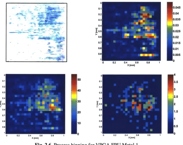
Another useful metric of manufacturability, demonstrated in Figure 2.6 for Metal 1 of the VPGA layout, is uniformity in feature sizes across a layout layer. One way to characterize this is to put feature sizes in a number of "bins," each bin holding a defined range of feature sizes. These bins can be extracted for each discretized region on a layout. By examining the binning plots of Figure 2.6, the relative percentages of feature sizes that fall within a certain bin can be seen. The narrower the range of the feature sizes are across a design, the less vulnerable such a design is to many manufacturing uncertainties, including copper dishing and oxide erosion, which can lead to plating and CMP variation [2]. For the VPGA evaluated here, over 90% of all
interconnect features in the design are grouped into Bin 1, or features smaller than
0.35
srm
in width. Along with the uniform pattern density across the metal interconnects, the process binning is optimal for manufacturability.0 0.045 0.2 0.04 0.3 0.035 0.03 0.025 0._ 0.02 0.7 0.015 0.8 0.01 0.9 0.005 0 0.2 0.4 0.6 0.8 1 0 X jmm] 004 01 50.1 3.5 0.2 0.2 403 0.3 0.3 2.5 3 1005 0 20 1.5 0.7 0.7 0.8 10 0.8 0.9 0.9 0.5 0 0.2 0.4 0.6 0.8 1 0 0 0.2 0.4 0.6 0.8 10 X [mm] X (MMJ
Fig. 2.6. Process binning for VPGA FPU Metal 1 interconnect. Metal 1 interconnect layout (upper left); Metal 1 interconnect pattern density (upper right); Bin 1
[0-0.35 gm] (lower left); Bin 2 [0.35-0.50 pm] (lower
right).
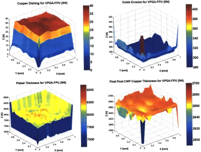
Moreover, when actual process models are run on the VPGA design, the results are dramatic. Based on models for copper CMP developed elsewhere in other work, we can predict how each metal layer will manufacture, for an example plating and CMP process [19]. Metal 4, which is one of the grid layers for the VPGA, was used to demonstrate the manufacturability of regular, repeated structures. Copper dishing, oxide
erosion, plated thickness, and post-CMP copper thickness models were applied to the
VPGA FPU layout to determine the degree of variation in processing. The results, shown
in Figure 2.7, highlight the uniformity of the processing involved. Ignoring the edge effects caused by the layout edge, the degree of variation is low relative to more irregular designs: final post-CMP copper plating thickness varies less than 3%, compared with up to 12% or more in some cases for custom ASIC designs.
Copper Dishing for VPGA-FPU (M4)
40,
N15
00
02 02
Y [nun) 0 0 G XTh F
Plate Thickness for VPGA-FPU (144)
40 35 30 25 20 15 10 5 0
Oxide Erosion for VPGA-FPU (M4)
420-1 400 380 N 340 320- 280-004 02 C k 0C2 G YuIwa 0 0 X Omni
Final Post-CMP Copper Thickness for VPGA-FPU (M4)
9000 7500 2M2 7000 2000 A06 0 00 06 0.4 0 02 P 0.2 0
Y c-lO 0 0 X ImnI Y Drn 0 0 x nunj
Fig. 2.7. Modeled copper thickness (upper left), oxide erosion (upper right), plated thickness (lower left), and post-CMP copper thickness (lower right) for VPGA FPU's
metal 4 interconnect. 400 380 360 340 320 300 280 2700 2680 260 2640 2620 2600 1
2.3
Berkeley Emulation Engine (BEE): A Semi-Regular Flow
The Berkeley Emulation Engine (BEE) project at the UC Berkeley Wireless Research Center is a system of flows and parallel FPGA processors for emulation [24]. Its goal is to speed the chip design to hardware verification process to a single day. Relatively well documented, the project uses an intelligent, semi-regular flow to optimize and layout an
ASIC design. It also utilizes an efficient dummy fill algorithm to reduce process
variation effects, and is thus an interesting candidate for design flow examination.
A semi-regular ASIC design flow uses standard cell libraries and algorithms to
optimize interaction distance, interconnect routing, pattern density, and many other measures to create as regular a layout as possible. Over multiple iterations, the placement tools in the flow decide on the optimal placement of standard cells. With an intelligent flow, these cells are then routed to achieve reproducible, optimal results. Both the VPGA and a BEE-generated ASIC are synthesized designs with standard cell routing. The BEE design, however, lacks the use of well characterized configurable logic blocks (CLBs) and a mesh interconnect routing grid, and thus comparison with potentially more regular designs such as the VPGA are of interest. A generated 4092-bit low density parity check
(LDPC) decoder [14] was chosen for comparison to the VPGA design. The metal 3
interconnect layer was extracted from the LDPC decoder and analyzed in the same fashion as its VPGA counterpart. The proprietary Praesagus extraction tool was used to extract a pattern density map from the design, as depicted in Figure 2.8. The design with and without dummy is evaluated for comparison.
From a manufacturability standpoint, a few things stand out with the BEE-generated decoder. The first is the impact of the dummy fill algorithms in the CAD flow.
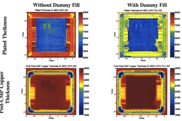
As mentioned earlier in this work, dummy fill refers to the act of inserting redundant blocks in each layer of a design to create a more planar surface after patterning and CMP. In this design, for example, dummy fill reduces oxide erosion variation on the die from
25% to 10% and post-CMP die copper thickness variation from 8% to 3%, as depicted in Figures 2.9 and 2.10. However, good dummy fill algorithms are increasingly complex and time and resource intensive to apply, limiting their widespread use.
0 Pgsmn Denay for sum 0.8 PAMr DMNy ftr 0.8
0.7 0.7 0.6 0.6 0.5 0.5 0.4 0.4 0.3 0.3 0.2 2 .0.2 0.1 0.1 2 0.5 1 1 2 Z .5 3 0 .5 1 1.5 2 2.5 0 0.5 nl 2 25 0 X Imn4
Fig. 2.8. Pattern density (with and without dummy fill) for BEE-generated layout.
Without Dummy Fill With Dummy Fill
Coppar Di.In for BEE-LDPC.M3 500 0 Copper D for BEE-DPC.FLLM3
400 400 300 300 200 200 100 100 00 25s 0 0. 1 15 2 2S 3 0 5 O A 1 A 2 2. 3 0 0 Oxide Erosion for BEE-LDPC.M3 o 0 Oxide Erosion for BEE-LDPC.FILLM3 850
0.5 700.5 . 750 * 700 700 650 650 600 1 600 550 2500 500
o
. 450 23450 o 05 1 15 2 25 4 400Fig. 2.9. Copper dishing and oxide erosion (with and without dummy fill) for BEE-generated layout.
Without Dummy Fill
Plted Thickness for BEE-LDPC.M3
0 800 7500 7000 5 6500 o as 1 1 2 2.5 3 8000 I [a"
Fine! Pot-CMP Copper Thicknes for BEE-LDPC.M3
2500 2400 2300 2200 2100 2000 - - 1900 1im0
With Dummy Fill Pietd Thickness for BEE-LDPC.FILL M3
050 0.s 7500 7000 2 .5 [ 0 a 1 10 2 Z 3 000
Fmal Poe0-CMP Copper Thickness for BEE-LDPC FILL.M3
0 2600 2500 0150 2400 1 2300 2100 2 2000 1900 .. .. .. 800 Xamqe XIDen
Fig. 2.10. Plated thickness and post-CMP copper thickness
(with and without dummy fill) for BEE-generated layout.
The second item of interest is the post-manufacturing topography of the pads and corners of the chip, seen in Figure 2.11. The steep drop in landscape surrounding the circuitry is not corrected by the dummy fill and contributes the greatest source of variation in the design. Although the decoder was designed within its technology's DRC specifications, this example illustrates that there is much room for manufacturability optimization. In such a design (1 mm2), as planar a surface as possible will ensure the most accurate CMP and process results. The penalties for poor processing may affect the pads in the form of throughput, adding unexpected coupling and delay in this high-speed chip design. Increased attention to dummy fill in the edge and pad boundary regions would lessen these post-CMP edge non-uniformities.
V AL V £ 00 la I
200 2600 2500 2500 2400, 2400 2200,2220 2210Z= 210 210 20M0 V50210
mea2 ayr ot-M.Wt3u umyfl2let n
1.50 1500
1000 2 1000
The semi-regular flow of the BEE must utilize a time-intensive dummy fill
algorithm process to create a layout that is comparable in manufacturability to the VPGA FPU examined. Despite the semi-regular nature of the flow and its use of standard cell libraries for routing, the post-CMP profile of the BEE-generated layout reveals that it is not as manufacturable, with respect to this class of pattern dependent process variations, as the VPGA examined previously. The regular architecture of the VPGA has intrinsic manufacturability advantages, including a grid interconnect structure and repeated blocks of standard cells. Nevertheless, it appears that a semi-regular flow, like that of the BEE, may be able to achieve comparable results with an advanced dummy fill methodology.
2.4 MIT Low Power FPGA
Up to this point, we have analyzed a novel regular fabric and a flow-generated ASIC. A last model for comparison is an established and well understood regular fabric in the form of an FPGA created by Honore and Chandrakasan [8], originally designed to apply circuit-level power reduction techniques for use in power aware systems. From the
VPGA examined before, we saw the effects of regularity in reducing system level pattern
density variation. With the Berkeley decoder, we witnessed the advantage of using dummy fill for reducing process effects. In this MIT FPGA, both elements are combined for reducing manufacturing variation significantly.
Metal I Density for MIT Honore/Chandrakasan PPGA (no dummy fill) Metal 1 Density for MIT Honore/Chandrakasan FPGA (with dummy fill)
0.9 0.9 0.8 0.8 2 2 0.7 0.7 0.6 0.6 S0.6 0.6 5 OA 5OA 0.3 0.3 0.2 0.2 0.1 0.1 0 1 2 3 4 5 6 7 a 0 1 2 3 4 5 a 7 a X [mm X [f""
Fig. 2.12. Pattern density (with and without dummy fill) for MIT FPGA.
With this design, like the Berkeley decoder, the most dramatic effects of dummy fill are at the edges. From Figure 2.12, we notice that without dummy fill the edge of the
FPGA die increases in pattern density from 0% to 38% to 60%, a poor gradient. This is
in comparison to the 30% to 50% to 60% gradient when dummy fill is used. Though throughput may not be as great an issue as with the Berkeley decoder, the subject of edge non-uniformity is nevertheless an important one that demands further review.
9000"
5000
4
Y Immi
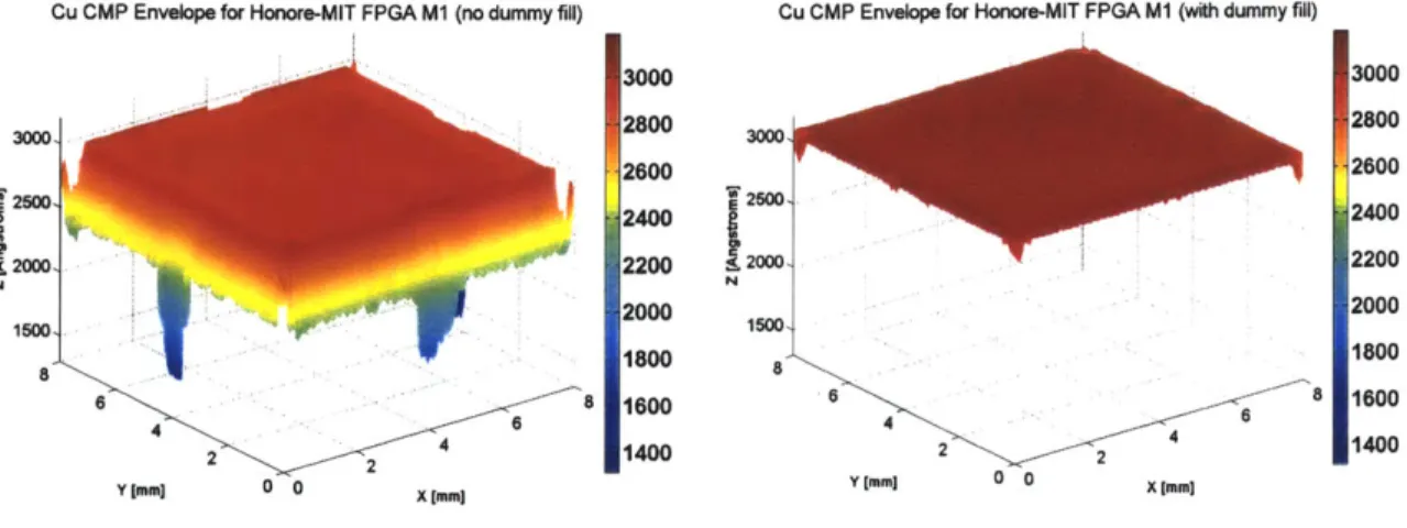
The dummy fill also creates a slimmer ECD envelope on the chip, and less ECD variation on the edges, as seen in Figure 2.13. After the copper CMP, the results may be dramatic, as depicted in Figure 2.14. When dummy fill is used in this regular layout, the predicted CMP envelope variation is reduced from 45% to near 5%. In terms of reducing manufacturing variation, this data suggests that the FPGA architecture contributes much less to the cause than the actual dummy fill placement. As this and previous results have indicated, design for manufacturability must address a solution beyond just the placement of regular blocks. Even an FPGA, which has traditionally been considered a highly manufacturable structure, may run into manufacturing problems related to these types of layout pattern systematic process variations.
9000 8500 8000 7500 7000 5500 5500
ECD Envelope for Honore-MIT FPGA M1 (with dummy fill) ECD Envelope for Honors-MIT FPGA M1 (no dummy fill)
9000
8500
8000
2 2 500
0 Xmm X [mm)0
Fig. 2.13. Electrochemical deposition (ECD) Copper damascene envelope profile for MIT Honore/Chandrakasan
Low Power FPGA. Without dummy fill (left) and with (right).
Cu CMP Envelope for Honore-MIT FPGA M1 (no dummy fill) 3000 2800 2600 2400 1800 6 6 1600 4 6 2 2 414 Y [1 0 0 X IMm
Cu CMP Envelope for Honore-MIl
2300
8
2
Y0 n
Cu CMP Envelope for Honore-MIT FPGA MI (with dummy fill)
1500
88 466
4 2 2
Y Imj] 0 0 xmm3
T FPGA M1 (with dummy fill)
3050 3000 2950
2900
2850 8 6 2800 4 2 [ X [mm]Fig. 2.14. 3D Visualization of MIT Honore/Chandrakasan low power FPGA, post-CMP. Without dummy fill (upper left) and with (upper right). Zoom of profile with dummy
fill (bottom).
2.5
Results Summary
Regular fabrics in circuit designs appear promising from a manufacturability perspective. Because it is made up of well-characterized, predictable, repeated components, a regular design is less vulnerable to process variations during manufacturing. Pattern-based 3000 2800 2600 2400 2200 2000 1800 1600 1400
dependency analyses of a via-patterned gate array (VPGA) interconnect layer confirmed the highly uniform pattern density of the structure and relative robustness to dishing and oxide erosion. Comparisons were made to a more traditional ASIC and FPGA, each with and without dummy fill, to evaluate the improvements in pattern dependency variation using such compensative layout techniques. Dummy fill does significantly planarize layers, as suggested by pattern density and post-CMP plating data, but potentially at a high capacitive cost that an intrinsically regular design, such as a VPGA, does not pay. Edge effects, and the impact of dummy fill in reducing them, were also examined.
Chapter 3
Exploring Regular Circuit Architectures
Shifting one step down from the system level to the circuit level, our next goal is to determine the potential impact of a regular circuit family in reducing systematic performance and process variation. Ultimately, isolating the robustness characteristics of each circuit family may deliver some understanding towards the impact of architecture choice on system level manufacturability. This chapter explores one such regular circuit style, that of limited switch dynamic logic, versus more traditional dynamic and static styles. The qualities that contribute to a regular circuit family are discussed and an adder design is introduced as a benchmark for further analysis in this research.
3.1
Limited Switch Dynamic Logic (LSDL) Architecture
Dynamic logic has traditionally been a faster performing alternative to static logic, though it trades power and robustness for its performance advantage [15]. Dynamic logic's clocked nature makes it more difficult to manage and introduces another dimension of variation that must be controlled for correct operation. More advanced forms of domino logic, like the dual-rail version, have been developed to solve many of the robustness problems, but power still remains a critical factor.
Domino Limited Switch Dynamic Logic
ua+bcaI OUtp
J eicst create
Fig. 3.1. Domino vs. LSDL schematics [10].
By introducing latches into the logic at every stage of a domino design, we can
generate what IBM has termed limited switch dynamic logic, or LSDL [25]. Typical schematics for domino and LSDL logic are depicted in Figure 3.1. There are numerous advantages to such a technique. Introducing an inverting latch into the logic essentially separates the logic stage from the gain stage. As a result, logic stages can be kept close to minimum size, and only the gain stages need to be sized, as suggested in Figure 3.2. The result is a much smaller design, which has promising cost implications. In this smaller design, cells more closely resemble each other, not only in size, but also in content. All cells include the same pattern of latching transistors and a similar pattern of (close to) minimum sized domino transistors. From a performance perspective, the LSDL clock can resemble more of a pulse than a standard domino clock, given the latching capabilities of the circuit. Duty cycle can be reduced well below 50%, allowing for higher speed designs. Moreover, the latched nature of the architecture ensures less activity through switching at internal nodes in the design, which can help reduce overall power consumption.
The concept of embedding logic functionality into latches is not a novel one. It was extensively used in the design of the EV4 DEC Alpha microprocessor and many other high performance designs [15]. True Single Phase Clock (TSPC) is a popular
method of integrating logic with latches. LSDL, though structurally similar to previous techniques, varies in its approach to clocking and circuit sizing, exploiting the regularity of this circuit topology in a way not considered before.
LSDL Sizing
- .Logic is nminimum size Only driving
latch/inverters sized
Integrated inverting latch
Domino Sizing
Fig. 3.2. LSDL sizing vs. domino sizing.
Though this circuit style has promising performance and power advantages over traditional static and domino designs, another interesting aspect is the regularity of such a style. There is logical regularity in the fact that there is separation of gain and logic elements and less internal switching, but there is also considerable layout regularity. Since logic is kept small, the majority of area in such a design would be taken up by the
LSDL latches, which themselves are simple, well-characterizable, repeated structures.
These principles were examined and an approach was established to examine the effect of the regularity of LSDL on not only performance, but also robustness to process variation and manufacturability. A comparison was made between domino, static, and
LSDL adders for the purpose of understanding the significance of this regularity better.
3.2
Domino and Static Circuits
A traditional domino or static circuit is not regular in sizing like an LSDL circuit may be,
logical robustness (i.e. low sensitivity to noise), good performance, and low power consumption with no static power dissipation [15]. The static circuit is therefore the classic comparison to use as a baseline when measuring robustness and reliability.
Advantages of dynamic logic include fewer transistors (thus fewer load capacitances to drive at each stage), increased speed performance, and no static power consumption. Disadvantages include increased overall power consumption, and an assortment of clock issues, including slew, clock feedthrough, and timing problems. Dynamic domino logic was used in this comparison for its similarity to LSDL, to quantify the extra advantages of the LSDL design compared to static logic.
All circuit styles were sized using the logical effort technique [15]. In a chain of
circuits, this method uses the fact that complex gates must work harder, or place more effort, to produce similar responses. As indicated before, only the LSDL design takes advantage of this principle, by integrating simple inverting latches, which themselves have low logical effort. Overall, since a chain sizing focuses on these inverters, overall design size is reduced. The static and domino designs do not possess this intrinsic regularity component.
3.3
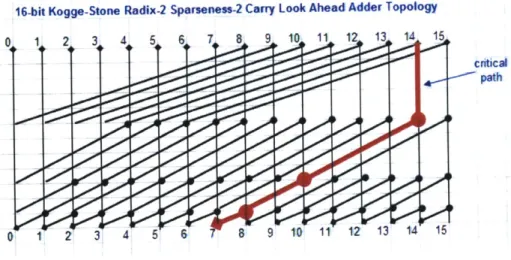
Adder Design
Adders are generally well understood designs, and quite regular structures. They are designed using blocks of logic in a repeated fashion and can be scaled to a larger size using more of these blocks. For these reasons, a 16-bit carry look ahead adder was a good structure to compare different circuit architectures against one another. By
variations, it is possible to understand the impact of design style on not only performance but manufacturability.
The 16-bit size for the adder was chosen to begin with, to be expanded to 32-bit if necessary. The simulation time per run had to be kept reasonable to complete the thousands of Monte Carlo runs planned for each adder in the limited time available. The carry-look ahead style was chosen for its speed and common use. The logarithmic nature of its computation ensures maximum speed and reflects modem adder designs. Higher radices in logarithmic adders reduce the number of stages, but make each gate more complicated. Higher radices are better for low fanout where intrinsic delay dominates. Sparse trees reduce the number of gates and wires, but increase the fanout on the internal nodes. Finally, a Kogge-Stone tree style was selected because these trees yield a minimum number of stages for a given radix [17]. With these considerations in mind, a radix-2, sparseness-2, Kogge-Stone CLA adder was selected for design. For n bits with radix r, this CLA architecture presents a logr(n) delay.
16-bit Kogge-Stone Radix-2 Sparseness-2 Carry Look Ahead Adder Topology
0 1 2 3 4 5 6 7 B 9 10 11 12 13 1 1
tritical
path
Fig. 3.3. Topology for 16-bit CLA adder design. Critical path is measured at SUM14.
Layout of the three adders in question was performed manually, optimized for density. The domino design has the characteristic of having mostly n-channel devices. The only p-channel devices are pre-charge transistors and auxiliary transistors, such as keepers or within inverters. Since all logic is sized throughout a domino sizing chain, this creates an increasingly large gap in the area of n-channel devices versus p-channel devices with a domino layout cell. A loss in pattern density results within larger cells.
16-bit Domino CLA Adder
Fig. 3.4.
16-bit LSDL CLA Adder 16-bit Static CLA Adder Adder layouts, by circuit architecture.
The LSDL design, though related to the domino design, can be optimized much more for density. The first major difference between the architectures is the minimum sizing of the logic transistors. The result is smaller, more modular transistors that can be used to fill small gaps in the layout. In a comparable domino design, these small patches would remain unused and dummy fill would need to be utilized to fill such gaps. Furthermore, integrated latches add more p-channel transistors to the mix and help to even out the balance of n-channel and p-channel transistors, thus eliminating the area discrepancy between these transistors within the adder cells.
![Fig. 1.1. Process variation types and sources [20].](https://thumb-eu.123doks.com/thumbv2/123doknet/14682708.559615/13.918.140.791.311.594/fig-process-variation-types-sources.webp)
![Fig. 1.2. Increasing geometrical primitives increases uncertainty in final design [1].](https://thumb-eu.123doks.com/thumbv2/123doknet/14682708.559615/16.918.290.659.116.427/fig-increasing-geometrical-primitives-increases-uncertainty-final-design.webp)