Design and Control of an Optical Fast-Scanning System for Silicon Wafer Feature Measurement
by Joseph C. Taglic
Submitted to the
Department of Mechanical Engineering
in Partial Fulfillment of the Requirements for the Degree of Bachelor of Science in Mechanical Engineering
at the
Massachusetts Institute of Technology
June 2018
2018 Massachusetts Institute of Technology. All rights reserved.
Signature redacted
Signature of Author:/epartment'of Mechanical Engineering May 18, 2018
Certified by:
Signature redacted
/oesr
Kamal Youcef-Toumi Professor of Mechanical EngineeringSignature redacted
Thesis Supervisor MASSACHUSETTS INSTITUTEOF TECHNOLOGY
SEP 13 2018
LIBRARIES
Rohit Karnik Associate Professor of Mechanical Engineering Undergraduate Officer Accepted by:
MIlLibraries
77 Massachusetts Avenue Cambridge, MA 02139 http://Iibraries.mit.edu/ask
DISCLAIMER NOTICE
The pagination in this thesis reflects how it was delivered to the Institute Archives and Special Collections.
The Table of Contents does not accurately represent the
page numbering.
Design and Control of an Optical Fast-Scanning System for Silicon Wafer Feature Measurement
by
Joseph C. Taglic
Submitted to the Department of Mechanical Engineering on May 18, 2018 in Partial Fulfillment of the
Requirements for the Degree of Bachelor of Science in Mechanical Engineering
ABSTRACT
Modem semiconductor manufacturing requires great precision for fabricating features on the surface of silicon wafers. However, testing of these wafers currently consists of selecting a subset of manufactured wafers and analyzing them with a scanning electron microscope. That process is slow and destructive to the tested wafers, and does not allow for examination of every wafer produced. This project seeks to develop an optical fast-scanning system for in-situ optical nanostructure measurement. This would be able to process many silicon wafers in a short amount of time, without destruction of the measured wafers. One key requirement for the project is thus the ability to scan a laser over the entire area of a silicon wafer in a short amount of time. Additional requirements include high precision, for accurate measurement, and adaptability to a variety of sample sizes. This thesis centers on the design and control of devices to attain these goals.
Different options for design of the system are explored, with approximate scanning speed and accuracy calculated for different configurations. From these, one layout is explored in detail. The design of this system as it would be constructed is described. Driving voltage waveforms that allow for galvanometer scanning of the entire wafer area are also specified. A geometric and programmatic model of the system shows that it would be capable of detection of features greater than 1.5 mm in size in the span of 5 minutes, with speed that is easily increased.
Thesis Supervisor: Kamal Youcef-Toumi Tile: Professor of Mechanical Engineering
Table of Contents Abstract 3 Table of Contents 5 List of Figures 6 1. Introduction 7 2. System Requirements 9 3. Design Possibilities 11
3.1 Actuated Stage Approach 1I
3.2 Actuated Laser Source Approach 15
3.3 Dual Actuation Approach 20
4. System Design 21 3.1 Laser Mount 21 3.2 Sample Mount 22 3.3 Receptor Array 23 5. Galvanometer Control 27 6. System Modeling 30
7. Conclusions and Recommendations 37
7.1 Conclusions 37
7.2 Recommendations 37
References 39
Appendix A: Components 40
Appendix B: Model Code 46
List of Figures Figure 2-1: Figure 3-1: Figure 3-2: Figure 3-3: Figure 3-4: Figure 3-5: Figure 3-6: Figure 4-1: Figure 4-2: Figure 4-3: Figure 4-4: Figure 4-5: Figure 5-1: Figure 5-2: Figure 5-3: Figure 6-1: Figure 6-2: Figure 6-3: Figure 6-4: Figure 6-5: Figure 6-6: Figure 6-3: 6
Data Collection Points
Stage with Two Rotational Actuated Axes Stage with Two Linear Actuated Axes
Stage with One Linear and One Rotational Actuated Axis Laser Mount with Two Linear Actuated Axes
Laser Mount with Two Rotational Actuated Axes
Laser Mount with One Rotational and One Linear Actuated Axis Laser Mount
Basic Wafer Mount Wafer Platform Mount Receptor Array
Geometric Representation of the Dome-Shaped Structure Wafer Coordinate System
Line-By-Line Scan
Scanning Control Waveform Parameterized Geometry Photodetector Points Detection Points
Histogram of Minimum Point Spacing Wafer Coverage Curve
Coverage Failure Points Detection Points 9 S1 12 13 16 17 19 22 23 23 24 25 27 28 28 30 31 32 33 34 34 31
1. Introduction
Many modern devices, from computers to phones and other everyday items, have been enabled by the invention and evolution of silicon-based semiconductors and transistors. These electrical components are responsible for the logic and storage that allows these devices to handle operations more complex than circuitry would otherwise allow. In the early age of computers, Intel co-founder Gordon Moore posited that every year, the density of these silicon-based components on a chip would double. [1] That exponential growth has held until recently, as manufacture of smaller and smaller components has become exceedingly difficult.
These components are manufactured in a multi-step process that requires high precision and minimal contamination. Doped silicon is first produced as a single cylindrical crystal of diameter slightly larger than the desired wafer diameter. The ingot is cut into slices slightly thicker than the final wafer thickness. The slice is trimmed, smoothed, and cleaned and is ready for use as a wafer for semiconductor and transistor manufacture. [2] In the transistor manufacturing process, silicon can be removed or other material can be added selectively using a variety of different masking, deposition, and etching techniques.
One difficulty faced by the silicon wafer and electronics component manufacturing industry is detection of features on the wafers during or after the manufacturing process. There are two main current methods of doing so: atomic force microscopy and scanning electron microscopy. In atomic force microscopy, the system consists of a sharp probe attached to the end of a small spring-like cantilevered beam. A laser reflects on that end of the beam, and changes in the reflection of the laser due to deflection of the beam allow the system to detect depth of nanometer-sized features on the sample surface. [3] In scanning electron microscopy, a beam of electrons is scanned across the sample surface and detections of secondary electrons can be used to determine the surface topology. [4]
Both of the aforementioned methods have several limitations. Both are only capable of scanning a fairly small area, with maximum sample size on the order of square millimeters. They also both share one crucial drawback: after analysis, a silicon wafer and the components on it are no longer useable. While this allows for feedback on the manufacturing process, a producer or consumer cannot guarantee the quality of a single silicon wafer or its features.
One option for an alternative scanning method is optical detection of features. The features on a wafer are too small to be detected using standard optical measurement as would be performed
with a standard microscope. However, it is hypothesized that by using scatterometry and interferometry, among other methods, the features on the surface of silicon wafers can be reliably and non-destructively detected with a resolution similar to that of the other methods. This involves shining a laser directly onto the surface of the wafer at various points and observing the reflected beam.
The author worked with a research group in the Mechatronics Research Lab at MIT studying optical detection of features on silicon wafers. One of the key challenges faced in this endeavor is the scanning mechanism for the laser. This thesis explores the various design options and technologies that might be leveraged for this purpose, and makes recommendations for design of an operational system.
The thesis is broken down into sections of varying length. The next section outlines the necessary functionality and details what the system seeks to achieve. A third section presents the different options that might be used to achieve those requirements. The fourth section presents a possible final setup for the scanning system, and the fifth specifies the control system for that setup. The final two sections present an analysis of the potential effectiveness of such a system and improvements that could be made.
2. System Requirements
The optical detection system has several requirements of the scanning subsystem. The most basic and fairly obvious requirement is that, for many points on the wafer, the system should allow for a laser beam to be reflected and detected. Additionally, these points must be spread out across the entire surface of the wafer. It is expected that the system will have high accuracy and repeatability as well. Two additional requirements are less technical in nature: first, that the system
be reasonably sized for laboratory production, and second, that the system complete a scan of a
standard size wafer in a reasonably short amount of time.
Operation of the scanning system consists of passing a laser beam over the surface of a wafer and collecting that laser after reflection for analysis. This analysis can determine the presence and size of features present on the wafer. A system should be able to do this for many points spaced throughout the surface. An ideal system would be able to do this for an arbitrary number of points. Some experimental solutions may compromise on this goal by specifying a minimum feature size. A grid with some spacing based on that feature size could be imposed on the wafer, such that features that are located at intersections on the grid are detected. As an illustrative example, an experimental setup might space these points across a standard wafer of 300 mm diameter in order to detect features of size 3 mm or larger. In reality, the features being detected are far smaller in size. Three possible layouts are illustrated in Figure 2-1.
-5 -1 - 5 1150 5 150 -1 -i 5 1 5 -5 -1 - 0 0 a 100 /... 50.. .3 .. ... t a s 506 -100. . . . . -100 /-10 ... . . 7... -1W0 -100 -50 0 5D 100 550 -150 -100 -50 0 so 100 ISO -150) 100 -50 a 50IS055
Figure 2-1: Data Collection Points. The graphs represent data points on the surface of a wafer with diameter 300 mm. The points in the left image correspond to a simple square grid layout, those in the
center use a radial pattern, and the points on the right use a spiral pattern to achieve a similar feature size. In this case, with feature size of 15 mm, the square grid uses 305 points compared to 351 with the radial pattern and 311 for the spiral.
The two unique challenges presented are the need for collection of the reflected beam and the size of the sample surface. In many applications of laser scanning, one or the other is required
but not both. For example, in applications like laser printing and engraving, the engineer must only ensure that the laser reaches the surface points that it intends to, but there is no need to collect a reflected laser; the beam, having reached the material, is no longer needed. On the other hand, in a similar application like scanning electron microscopy (which uses an electron beam rather than a laser beam) the area of scanning is an order of magnitude smaller - a 2011 paper describes a method for acquiring "large-scale" automated SEM data, and describes the process of scanning a 4 cm x 2 cm sample as indicative of the intended scale. [5] A 300 mm diameter Silicon wafer has 88 times the area, and its diameter is 67 times the length of the rectangular sample's diagonal. Not only does the total area of scanning need to be greater, the distance that must be traversed is also greater.
Accuracy and repeatability are crucial to the success of the scanning system. For a laser scanning system, the resolution of the readings is partially determined by the diameter of the beam. In the optical system being developed, the beam in use is a 3.5 mm diameter beam that can be expanded or narrowed by optical devices. While intensity is not uniform across the cross section of the beam, and peaks in the middle, the resolution of any laser scanning process would be limited by this distribution of reflected light. Measurement of nanoscale features would likely be extremely difficult if not impossible with such a wide beam, as millions of features could be present at any given beam location. Future iterations of this optical scanner may use a beam contraction mechanism in order to achieve higher resolution.
For commercial use, the feature detection system should both be portable and able to process a wafer in a short amount of time. These characteristics would allow this form of testing to be integrated fairly seamlessly into the manufacturing process. Five minutes was decided upon as a reasonable target scan duration, and the ideal form factor is fairly small, such that it could be operated on a tabletop.
The scanning system must foremost provide reflection and collection of points across the surface of the wafer. The manner in which data collection occurs should furthermore be repeatable, and resolution is limited by the diameter of the laser beam. The final goals of system size and scan duration would enable the system to be adopted by component manufacturers.
3. Design Possibilities
The scanning system can be broken down into three components. The first of these components is a laser source and steering mechanism. The second is a structure for mounting and moving the wafer. The last is a laser collection and detection device. Between the first two devices, movement must occur in two axes in order to have one laser pass over the entire wafer. Design options for these two components have been divided into three potential configurations: both axes actuated through the wafer stage, both axes through the laser device, or one axis actuated through each device. Each approach has its strengths and weaknesses. The following sections each address one approach: first, actuation of solely the wafer stage; second, actuation of solely the wafer source; and third, actuation of both devices.
3.1 Actuated Stage Approach
The first approach mentioned would be to make the laser source static and actuate the platform on which the wafer is mounted. In order to get a 2-dimensional scan of the wafer, two axes of movement would be needed. There are three distinct options for the choice of axes: two rotational axes, two linear axes, or one linear axis, and one rotational axis.
It would be highly impractical, and ultimately ineffective, to use two axes of rotation of the wafer. Regardless of the choice of axes, this system fails to leverage the relative two-dimensionality of the wafer in order to minimize the complexity of the motion. Depending on the design of the setup, such a system would likely be extremely sensitive to slight changes in angular position either near the center or at the edge. Moreover, the angle of incidence of the beam on the wafer would be regularly changing, and this would necessitate a system of multiple detectors or actuation of the detection device as well. This is a need avoided by the other two actuated stage systems.
Figure 3-1: Stage with Two Rotational Actuated Axes. In this configuration, the laser reflection is irregular and the scan is likely unable to cover the entire wafer despite two axes of movement.
Use of two linear axes of movement seems like the simplest solution. The laser source and sink could remain fixed while the wafer would move solely in a single plane. This would entail mounting the wafer on a stage with 300 mm of movement in two directions, or using two stages in series, each with a range of motion of 300 mm. The scanning pattern would likely be a line-by-line scanning pattern that only requires movement in one axis at any time. There are a number of reasons such a system is unfeasible. One limitation is the lack of pre-existing stages that translate distances that far. A new system would have to be devised for translating the wafer across the tabletop. The primary failure of such a system would likely be the speed at which the wafer could be moved. Additionally, the system would consume a large working space and due to the scale of the movements, positioning might not be sufficiently accurate. These limitations are addressed by using a planar system with both linear and rotational movement.
Figure 3-2: Stage with Two Linear Actuated Axes. In this configuration, the laser consistently reflects to the same point. This method of actuation takes up a large surface area, and would be fairly slow. The range of motion also places limits on the system's accuracy.
Using one linear and one rotational axis of movement seems a better solution than each of the previous configurations. It is assumed that the angular displacement would occur as yaw, rotating the wafer around its radially symmetric axis. This significantly reduces the working area. With 360 degrees of rotation, there would only be a need for a radius length of translation in a single direction; with 180, there would only be a need for a diameter length. This system would improve upon the speed and space limitations of the solely linear system, and would similarly maintain a constant angle of incidence on the wafer such that no motion of the laser source and receiver are required. Of the options for stage actuation, this is likely best.
Figure 3-3: Stage with One Linear and One Rotational Actuated Axis. The laser consistently reflects to the same point. This method of actuation takes up a smaller surface area, and would demonstrate fairly high accuracy despite the need for long-range linear motion. However, it does also place heavy requirements on the ability of the system to secure the wafer.
These systems, especially the latter system featuring a linear axis and a rotational axis of actuation, could meet the system requirements while offering good speed and accuracy. The main issue with a moving stage, in that and the other configurations described in this section, is securing the wafer. The wafer must be secured regardless of the system design; however, the difficulty of keeping the wafer stationary relative to its stage increases significantly when the stage is moving. Part of the source of this difficulty is that one surface of the wafer must be exposed, and so any fastening device can only be applied to one side. This, combined with the need for fastening to be strictly temporary and nondestructive, makes fastening a fairly difficult problem. Two potential solutions would be a vacuum system that holds the wafer to the stage with suction or use of tape to secure the wafer in place. Both of these fastening systems are unreliable at best, and it would be difficult if not impossible to detect slippage of the wafer during rapid motion.
A potential stage system would incorporate a fastening system with components that could move the wafer with fairly high accuracy. The system would use a linear stage in tandem with a rotary stage, likely mounting the rotary stage on the linear stage and the wafer on the rotary stage. Newport Corporation, a supplier of scientific equipment, makes both types of stages with fairly high accuracy. A Newport 300-mm travel distance linear stage offers resolution of 1.25 pm and typical accuracy of 2.5 pm. [6] A rotary stage using a stepper motor, also produced by Newport, offers resolution of 0.2 mdeg, and typical accuracy of 8 mdeg. [7] Information about these components can be found in Appendix A. The resolution of the rotary stage would, with perfect fastening, be about 0.5 gm at the edge of a 300-mm diameter wafer, and its accuracy would be about 20 pm, giving the scanning system as a whole typical accuracy of 22.5 pm and resolution of 1.25 pm. The accuracy and repeatability would be suitable for the feature detection system; however, the scanning speed may be a limiting factor.
One key output of any configuration is the speed with which scanning can occur. This can be estimated based on system parameters. There are two general ways in which scanning can occur with the described setup. The first is to scan "ring-by-ring", in which the distance from the center of the wafer to the scanning point is held constant for a single pass and subsequent passes change this distance.
27T
tscan =
-rwafer %move * diaser
where tscan is the time to scan the wafer in seconds
n is the number of passes required
co is the radial speed of the rotational stage, in radians per second
rwafer is the radius of the wafer, in mm
diaser is the diameter of the laser, in mm
%move is the ratio of the change in distance from the wafer center
between passes, to the laser diameter. At 100%, there is no overlap between consecutive rings of the scan.
21r
Using this pattern and parameters of o = 400/s = 2- rad/s, rwafer = 150 mm, daser 3.5 mm,
and %move = 50%. The scanning pattern requires 86 passes, and using the above equations takes 774 seconds.
The other possible scanning pattern for this configuration is a radial scanning pattern, where each pass starts at the center of the wafer and scans towards the edge, and consecutive passes vary minutely in angle.
tscan = nrf
2
7Trwafer %move * diaser
where tscan is the time to scan the wafer in seconds
n is the number of passes required
rwafer is the radius of the wafer, in mm
v is the linear speed of the linear stage, in mm/s
daser is the diameter of the laser, in mm
%move is the ratio of the distance between the centers of scan points
on the edge of the wafer, to the laser diameter. At 100%, there is no overlap at the edge of the wafer between consecutive passes.
At v = 100 mm/s, and using the same other parameters, this method would take slightly longer at 539 passes requiring 808.5 seconds. The passes exhibit significant overlap at the center, and some adjustments could be made to reduce this time further; it is unlikely that the system would reach the prescribed 300 second goal. This configuration does not meet the basic system requirements, and would have even worse performance moving forward as the laser diameter is reduced.
Actuation of the wafer stage could be a reasonable method for scanning the device. The accuracy and repeatability of a sample system were shown to be fairly low, and it drastically simplifies the optical portion of the system by maintaining the angle of incidence of the laser on the wafer. The key failure of such a system is the time to scan. A faster rotary stage with lower resolution and similar accuracy could be used, but this would incur additional cost and would only be able to reduce the scanning time by roughly a factor of two. The other drawback would be the insecure fastening methods that might not keep the wafer in the correct position with respect to the stage platform.
3.2 Actuated Laser Source Approach
Another annroach to scanning a wafer consists of moving the laser source, or moving
mirrors that direct the beam, instead of moving the wafer itself. The most notable advantage of this approach over the motorized stage approach is that the wafer is generally exposed to less motion and vibration that could cause it to move during the scanning process. However, movement of the laser source also creates the challenge of how the receiver should be deployed. In most stage actuation schemes, the laser was fixed and the angle of incidence was constant, so the receiver could also be fixed. With an actuated laser source, the receiver must either also be actuated in order to detect the laser at different points, or the receiving device must span a wide range of inspection points and incidence angles. Similar to the case of the actuated stage, movement must occur in two axes: two linear, two rotational, or one of each.
Movement of the laser source along two linear axes is the simplest solution optically. A subsystem could be constructed that contains both the laser source and a receiver, oriented such that at the correct distance from the wafer the laser reflects to the receiver. This single device would be translated across the surface of the stage. Assuming that the motion is perfectly planar and that the wafer remains still, this would cause a constant angle of incidence on the wafer at all points.
Figure 3-4: Laser Mount with Two Linear Actuated Axes. The laser source and sink must be moved in tandem in order to guarantee detection. The main drawback of such a system is speed; linear actuators cannot achieve speeds fast enough to keep the scanning time low.
This system would make use of two linear motion systems, such as those sold by Thomson Linear, to actuate each direction. The technical details for these systems are available in Appendix
A. Thomson does not provide accuracy for their devices, but does give a measure of repeatability;
their best devices have 10 prm repeatability, worse than that of the previously described actuated stage. What these devices lack in repeatability, they make up for in speed. The maximum speed of a seemingly typical linear motion device is 0.25 m/s. [8] Using the below equation with 50% movement and 250 mm/s carriage speed, the scan could be completed in roughly 161 seconds. This assumes that the carriage is generally moving at its maximum speed, and that adjustment from one row of scanning to the next takes an insignificant amount of time. This is a vast improvement over the actuated stage, although it too is sensitive to the beam diameter.
1 Awajer
tca =tscan %overlap v
* diaser
where tscan is the time to scan the wafer in seconds
Awafer is the area of the wafer, in mm2 v is the linear speed of the carriage, in mm/s
diaser is the diameter of the laser, in mm
%move is the ratio of the distance between the centerlines of consecutive passes, to the laser diameter. At 100%, there is no overlap between consecutive passes.
The alternative solution is a system that keeps the laser source at a given point in space but varies the two planar angles at which the laser leaves the source system. This is a very common practice in laser scanning systems, and as such there are numerous devices that are designed to
achieve this goal. A drawback to this system, however, is difficulty of laser reception. The angle of incidence varies with the point on the wafer that is currently being analyzed, and there is no single receiver position relative to the plate or to the laser source device that guarantees the laser will reach it. Nevertheless, the availability of systems that achieve this actuation make it a favorable option. Generally, the two axes of rotation are achieved by a mirror with two axes of rotation or two mirrors each with one axis of rotation. The first case is typical of high-performance piezo-actuated mirrors; the second case is typical of galvanometer scanning units.
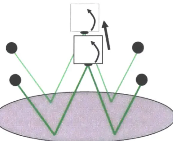
Figure 3-5: Laser Mount with Two Rotational Actuated Axes. Exclusive rotation of the laser device, or
of mirrors reflecting the laser, is by far the fastest way to move the laser point across the surface of the wafer. This can be achieved by either a piezo-actuated system or a galvanometer-based system. The main drawback, depicted here, is the wide range of paths that the laser can take as the orientation of the laser varies.
Piezo-actuated mirrors are capable of scanning incredibly quickly. Piezo actuators consist of a piezoelectric material that expands or contracts nearly unidirectionally when a voltage is applied. To achieve dual-axis scanning, a piezo system would consist of two or four stacks placed behind a mirror such that the differential in their lengths creates an angle with respect to a neutral plane. There are numerous difficulties encountered in implementing a piezo system. Piezo materials exhibit nonlinear behavior, making control fairly difficult. Additionally, the expansions and contractions are miniscule and cannot create a sufficiently large angle for scanning of a large wafer. For example, Physik Instrumente, a leading manufacturer of piezo systems, offers a 2-axis
scanning mirror, but the beam angle is limited to 35 mrad in both directions, for a total angle of
just 4 degrees. [9] Specs and other information about these mirrors can be found in Appendix A. In order to cover the entire surface area of the wafer, this device would have to be 4 meters away from the sample. This both enlarges the system to a nearly unusable point and largely neutralizes the benefit of the device's angular accuracy and repeatability. The beam angular resolution is given as 0.1 [trad, which corresponds to a wafer distance resolution of .43 prm at that distance; the
repeatability of I prad corresponds to 4.3 pm repeatability on the wafer. This performs better than both previously described systems, but is unfeasibly large. A common alternative for larger-scale scanning systems is a galvanometer scanning system.
A 2-axis galvanometer scanning system uses two mirrors to reflect a beam twice and
achieve planar scanning. A galvanometer is a device that can be used to measure the current flowing through a wire. It does this by placing a coil of wire in a magnetic field; when a current passes through, the coil rotates. The magnitude of the rotation is proportional to the current passed through the wire, and thus the device can give a reading of the current by observing movement. This type of device is used in galvanometer scanners by sending a known voltage, and a corresponding current, through the coil of the galvanometer. The coil is attached to a shaft that rotates to the angle corresponding to the given current. In this case, the shaft is attached to a mirror that can deflect the laser. In most systems, a reference voltage that corresponds to a desired angle is supplied to a controller that then uses feedback from the galvanometer to achieve that desired angle quickly and accurately. A dual-axis galvanometer-based scanning system can be achieved
by placing two galvanometers with attached mirrors such that a laser reflects off one mirror and
then the other. One such system is distributed by Thorlabs, an optical supply company. Their small beam diameter unit is capable of angular deflections of 250, so minimum distance above the working surface is only 32 centimeters. [10] The galvanometers also have a mechanical angular resolution of 0.00080 or 15 prad. Optical, mechanical, and electrical information about these devices can be found in Appendix A. However, because the device is closer to the surface of the wafer, the resolution on the wafer is 4.8 pim. The repeatability is also 15 pirad, giving a repeatability of 4.8 pm as well. This is lower resolution than the piezo system but similar repeatability, with the advantages of not taking up as much space and exhibiting almost perfectly linear behavior.
The galvanometer system also has the advantage of speed, when compared to the previously described linearly actuated system. Fast scanning applications typically use galvanometers for their high accuracy and speed. The galvanometer scanning unit previously mentioned has a full scale bandwidth of 175 Hz for a triangular wave, which is likely what would be used to operate the mirrors to scan in a line across the surface of the wafer. That suggests that one pass across the diameter of the wafer can be completed in 1/175 of a second, and smaller lines could be completed in even less time. Assuming use of a 3.5 mm diameter laser and 50% overlap between passes, only 172 passes are needed and in theory the scanning could be done nearly
instantaneously, in roughly a second. In this respect, the galvanometers vastly outperform the other systems mentioned.
Another option for actuation of the laser source system is to use a single axis of translation and a single axis of rotation. The translation would be supplied by a linear motion system, as described in reference to the dual-linear-axis system, and the rotation would likely be achieved by use of a 1-axis galvanometer scanner. Row-by-row scanning with this device would use the galvanometer to scan a row and the linear motion actuator to step from one row to the next. The accuracy and repeatability would thus be similar to the previously described systems, with only one axis of variation of the angle with which the laser hits the wafer.
Figure 3-6: Laser Mount with One Rotational and One Linear Actuated Axis. Because the bulk of the movement of the laser point on the surface of the wafer can be done by rotating the laser diode or the mirror, as in a galvanometer-based system, the speed reduction is not overwhelmingly significant in this arrangement. This setup would slightly contribute to simplicity of the system, as the location of the detector relative to the actuated laser would be constrained to a single plane.
Either of the galvanometer-based systems would achieve seemingly arbitrarily fast scanning of the wafer. However, both of them come with a separate difficult design challenge: detection. There are two possible solutions to this engineering problem. The first solution is to provide actuation for the receiving component such that, based on the prescribed orientation of the laser source, it is always at a point that the laser reflects to. For galvanometer scanning solutions, this would drastically increase the amount of time necessary for scanning as the movement of the receiver could not occur at nearly the rate at which the galvanometer system could scan. The alternative option is to design a structure that either uses mirrors to redirect the laser towards a single receiver or uses many receivers at various points above the wafer in order to detect the laser. The system of many receivers is unlikely to be successful for high-resolution systems, as each receiver would likely only produce meaningful output for a single point on the wafer. A system in
which all beams are reflected back to a single point, on the other hand, is slightly unfeasible and must be highly precise.
3.3 Dual Actuation Approach
The intermediate between sole actuation of the stage and sole actuation of the laser source would have each device capable of one axis of movement. In theory, this combines advantages and disadvantages of both systems. This could be implemented in a variety of ways. One option is linear motion in perpendicular directions, another is dual rotation. Dual rotation would likely be the simplest and most space-effective solution, with the wafer free to rotate about its central axis and the laser directed by a single-axis galvanometer. However, such a system would raise both previous concerns. Any system in which the wafer mount is actuated will have the same issue with unreliable fastening mechanisms; any system that uses a galvanometer or similar device to vary the beam direction will need a receptor array or an actuated receiver. Ultimately, there is little to be gained by choosing to actuate both the stage and the laser source and it doesn't obviate either of the difficulties previously encountered.
The three options for choice of device to actuate were dual-axis actuation of the wafer, dual-axis actuation of the laser source device, and single-axis actuation of both devices. Any system in which the wafer is being actuated exposes the wafer to movement and vibration that may move the wafer from its original position in an unexpected fashion. For this reason, the simpler approach is to actuate only the laser source device. This device is less prone to error from vibration and movement because the methods of fastening the components of the device are less constrained; that is, the laser and the galvanometer can be securely bolted or clamped into place, while the wafer would have to rely on tape or suction.
The two axes of movement for the laser steering system can be designated either linear or rotational. Linear actuation provides a greater degree of regularity for the scanning process, but is severely limited in its speed. Crucially, as the beam diameter gets smaller to increase resolution of the feature detection system, the scanning time of the linear system quickly grows beyond the five minute limit while the scanning time of the galvanometer system grows at roughly the same proportional rate but stays much lower. A system design for using the 2-axis galvanometer is discussed in the following sections.
4. System Design
The proposed scanning system uses the 2-axis galvanometer scanner mentioned in section IIB to pass the laser over the wafer. The two distinct approaches for detecting the laser after reflection are an actuated receiver system, or an array of mirrors and/or receivers that would collect the laser after reflection. An actuated receiver system would limit the speed with which scanning could occur, as translation around the wafer would certainly occur more slowly than rotation of the galvanometer mirror. As such, the proposed system uses an array of receivers to detect reflected lasers. This system features a galvanometer placed vertically above the center of a stationary wafer laid parallel to the tabletop, and a dome-like structure embedded with receptors to detect laser reflection.
This proposed system meets the speed requirements easily and achieves fairly high accuracy. The speed of the galvanometer system was described previously; the galvanometer can scan across a diameter of the wafer in less than one hundredth of a second and as such would not be the limiting factor in a scanning application. It is more probable that the speed of data acquisition would be instead limited by the sampling rate. The accuracy of the scanning system
would he 4.8 microns, as previously calculated. The resolution of the scanning is largely
dependent on the detectors, and is not directly correlated with the mechanical design of the system. The three components of the system are a mount for the laser diode and galvanometers, a stationary platform to hold the wafer, and a receiver array. These will be described independently.
4.1 Laser Source
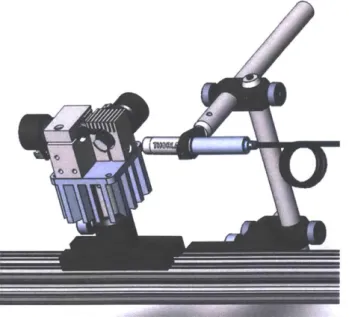
The laser diode and scanning galvanometer unit are mounted above the wafer. In order to prevent the laser from being unable to reach the edges of the wafer, the distance from galvanometer to sample is a few centimeters greater than the minimum distance. The laser and galvanometer are mounted using standard Thorlabs optical posts attached to a T-slotted framing rail, and must be aligned before use. One of the difficulties encountered is the fact that the provided mount for the galvanometer unit places the beam input point off-center; due to this, the laser source must be capable of adjustment in two directions. Once the devices are mounted, the rail can be attached to other framing components in order to be suspended over the wafer. The laser is supported by short cantilevered beams, which may be prone to vibration. Due to the size of the posts, however, this vibration is expected to be minimal. If necessary, steps can be taken to minimize the vibration of the laser diode and (to a lesser extend) the mounted galvanometer. Figure 4-1 shows this design.
Figure 4-1: Laser Mount. The laser is mounted on a series of posts with adjustable positioning to ensure that the laser is directed properly towards the galvanometer mirrors. The mirror is not aligned with the galvanometer post, requiring multiple axes of translation for the laser. The laser mount is cantilevered and may be prone to external vibration; additional steps can be taken to introduce damping to the system that reduces the vibration of the laser and galvanometer.
4.2 Sample Mount
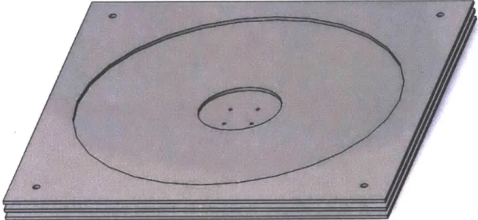
The second component is a wafer mount to ensure the position of the wafer during the scanning. The key design features of the wafer mount are repeatability between scans and adaptability to different size wafers. These are achieved through use of acrylic sheets to locate the mount on an optical breadboard and constrain the wafer. A base sheet with four holes for bolting into the breadboard is a constant component; a sheet with a hole for the wafer and four mounting holes can be placed on top of this sheet to ensure wafer location. The wafer fits snugly into the upper sheet hole to ensure a constant wafer location for scanning. The use of a separate upper layer allows for different size wafers to be used, by using a laser cutter to produce an identical sheet with a smaller central hole. This design is shown in the following figure.
Figure 4-2: Basic Wafer Mount. The mount is fastened by screwing into an optical breadboard, and the wafer is kept in place by the upper sheet. The acrylic sheets are squares with each side measuring 350 mm with a 300 mm diameter cutout. The screws are %"-20 screws for mounting on an optical breadboard.
This wafer mount design is also expandable to cases in which the wafer might be mounted on a kinematic mount. A third sheet could be added under the lower layer that would provide an interface with an adjustable platform, and then nuts could be used to bolt the sheets together instead of screwing into the breadboard. If the external mount requires bolts centrally located on the wafer mount, material can be removed from the initial bottom sheet in order to accommodate the bolt heads without compromising the positioning of the wafer, as demonstrated in Figure 4-3.
Figure 4-3: Wafer Platform Mount. The mount is fastened to the platform by screwing into the platform; the wafer is kept flat relative to the platform by a spacing sheet.
4.3 Receptor Array
The third component is a structure designed to be embedded with many receptors, in order to detect the laser as it scans over the surface of the wafer. In this design, the receptors are assumed to be fairly small and inexpensive; this assumption may not hold true as information about the
reflected laser may need to be collected by more complex devices. For the purposes of this design, the receptors are assumed to be photodiodes. In order to have the spacing of photodiodes necessary for reasonably complete detection, a dome-like structure is proposed in which the photodiodes would be embedded. The skeleton of such a dome would likely consist of plastic rods and 3D-printed connectors, which mechanically supports several 3D-printed circuit boards that provide access to the photodiode. From a data collection standpoint, each board would contain circuitry that bundles the signals from the photodiodes together and sends that signal to a central controller, which would then bundle signals from different boards to be passed to a computer for collection. The geometric alignment of these boards would look similar to the dome in Figure 4-4.
Figure 4-4: Receptor Array. A dome-shaped structure to mount photodetectors. Detectors such as photodiodes or phototransistors can be placed on the inside of the dome to detect light reflected off the wafer. This allows for laser detection at discrete points on the wafer. The panels are supported by a frame of plastic rods with custom joints at the corners. However, the reflected laser cannot reach detectors if directed at an edge.
The exact dimensions and geometry of this geodesic dome of triangular faces is informed
by needs of the scanning system. First, the distance across the octagonal base was decided to be
340 mm, in order to accommodate a 300 mm wafer comfortably. A second assumption was that the same size board should be useable in both the lower and the upper half of the dome. This would
in theory allow for less variation in the boards that would need to be printed and reduce cost by ordering in bulk. A third assumption was to evenly divide detection area between the lower half and the upper half. That is, the 8 boards that make up the upper half are responsible for detection when the laser falls less than roughly 100 mm from the center, and the lower half is responsible for detection for when the laser falls more than 100 mm from the center. These design assumptions and decisions informed the dimensions of the structure.
B
BOTH
Altitude: 188.5 mm Width: 131.2 mmB
L
L
SIDE VIEW, FLAT
LOWER
Altitude: 186.7 mm Width: 140.8 mm
TOPVIEW
Figure 4-5: Geometric Representation of the Dome-Shaped Structure. The structure is composed of two sizes of panel: a "both" size, that is used in both the lower and upper layer of the dome, and a "lower" size, that is used exclusively in the lower half. The larger size of the octagonal base of the lower half necessitates triangular panels with wider bases. The panels are arranged as shown and placed with edges coincident such that there are no gaps in the lower half, and some gaps in the upper half.
Laser reception using the dome has both strengths and weaknesses. The strength of using stationary receptors is that the galvanometer can scan with great speed, limited only by the sampling rate of the electronics used for data collection from the dome. There are a few weaknesses to this design approach, however. First, there are blind spots on the wafer such that the photoreceptor dome will not detect a laser directed at those spots. These are concentrated in the center and the areas that correspond to the spaces between panels in the upper half of the dome. Second, the resolution of the scanning device is limited by the spacing of photodetectors on the dome. The detectors chosen are photodiodes, which generate a voltage when exposed to light in
the proper wavelength. For the initial design, using a 532 nm laser, the photodiodes would detect green light in a wavelength range centered near that value. Photodiodes manufactured by Luna Optoelectronics detect light in the 350-1100 nm range and are easily placed on circuit boards using surface mount technology. Each photodiode has a footprint of 1.5 mm by 3.2 mm. [11] With the small form factor described above, the spacing of photodetectors would limit the smallest detectable feature size to around 1 mm. Other concerns include the stability of the dome over time, and the electronic complexity that would result from the vast number of photodiodes necessary. An analysis is done in the following section to determine how severe the two quantifiable limitations are. One solution to the spacing problem is to increase the size of the dome; after proving feasibility with a dome of the prescribed size, a larger dome could be used with similar receptor spacing that would achieve higher resolution on the surface of the wafer.
The strength of this system as a whole is the speed with which scanning can occur. By using a fast scanning galvanometer mirror system and a collection of stationary receivers, the scanning time is more dependent on the sampling rate of the data acquisition system than the mechanical speed at which the laser can be moved across the wafer. However, it does have its limitations. The resolution is limited by the density of receptors on the inside of the dome, and there is a decent area on the wafer that cannot be scanned. Both can be ameliorated by adjustments to the design, such as adding more boards or expanding the size of the dome. For initial modeling of the system, however, these adjustments will not be performed.
5. Galvanometer Control
The two galvanometer mirrors are controlled by specifying two input voltages, that are
each proportional to the angle output of one mirror. A Cartesian coordinate system coincident with the surface of the wafer and its origin at the wafer's center can be used to specify the scanned points. In order to scan the whole surface of the wafer, a waveform must be constructed that rotates the mirrors properly. In order to do line-by-line scanning, one mirror bears responsibility for setting the line along which to scan and the other allows for movement along that line. For simplicity, it will be assumed that the x-axis mirror sets the x-coordinate for a vertical line in the (x, y)-plane of and the y-axis mirror moves the reflection point along that line.
The two angles are calculated as functions of the wafer coordinate (x, y) and galvanometer
height hsource as follows:
0,, = tan- ho
hsource
tan' (hsource)
where hsource is the height of the laser source point
x and y are the coordinates of the point in the Cartesian coordinate system on the surface of the wafer
Ox and 6, are the angular positions of the galvanometer mirrors
0
Figure 5-1: Wafer Coordinate System. The points are described using a Cartesian coordinate system, which corresponds to values for the two angular quantities.
The pattern of scanning is a line-by-line scan as described in the figure below. The parameter that determines the frequency of the waveforms that specify the angular offsets of the galvanometer mirrors is a spacing parameter in units of length. The points on the wafer are laid out in a square grid with the given spacing, and the laser scans from point to adjacent point in a
line-by-line pattern. Because of the above relationship between the scan point and the mirror angle, constant speed movement on the wafer is achieved with waveform in the shape of the inverse tangent curve.
Figure 5-2: Line-By-Line Scan. The device scans in a single direction at any given time, adjusting the position of the scanning point between passes. While it does have some downtime during adjustment, the benefit of this pattern is simplicity as the laser must only ever move in a single direction.
Depending on this spacing, the waveform for the y angle may appear fairly linear, especially given the limited angle that is scanned. Decreasing the spacing increases the number of points and causes the mirrors to scan more quickly. If the number of waypoints scanned divided
by the duration of the scan is greater than the sampling rate of the data acquisition electronics, this
may cause irregularities in data collection that limit the effectiveness of the scanning system. With a spacing of 1 mm, the waveforms use 70,661 waypoints; this corresponds to a minimum sampling rate of 236 Hz. These values increase quadratically as the spacing decreases; with 0.4 mm spacing, the waveforms use 441,763 waypoints and require sampling at 1.5 kHz.
Dual Waveform for Wafer Scanning, Fuil Waveform 1402 -01 t210 401 10--40 148 '5 1455 55. 1505 '5 55 152 T.".
Figure 5-3: Scanning Control Waveform. To achieve line-by-line scanning, the waveform in one direction steps from one line to the next while the other is responsible for scanning each line. The red curve corresponds to the stepping waveform while the blue represents line scanning. The upper graph shows the entire 5-minute scan, while the lower shows three lines of scanning at the middle of the wafer. While both should approximate inverse tangent functions, the stepping waveform appears to have opposite curvature due to short step durations at either end of the scan and the linear waveform has low curvature in the angle range of the galvanometer.
The angle of the galvanometers is controlled by a voltage signal from an arbitrary
waveform generator, with a voltage-to-angle ratio that can be set by the operator. The setting that allows full use of the 12.5 degree mechanical scan range is scaling of 0.8 V/degree, so the output of the signal generator should appear nearly identical to the shown waveforms, with differing scale. Making full use of the angular range allows the galvanometer to be placed as close as possible to the wafer surface, enhancing scanning by reducing repeatability errors.
6. System Modeling
The described system lacks a definitive measure of resolution. Depending on the number and spacing of detectors, the resolution of the system varies greatly. To provide a measure of the potential resolution of such a system, a geometric model was developed. This model makes several assumptions about the behavior of the system. First, it models the galvanometer scanning device as a point source; in reality, because of the offset between the two mirrors, the laser emerges from the galvanometer with an offset that varies slightly with the angle of the mirrors. The other assumptions are consistent with proper construction of the structure. First, it is assumed that panels with embedded detectors are connected perfectly at their corners. It is further assumed that the specimen lays perfectly flat, and that the base of the dome is coplanar with the exposed face of the specimen.
The dome can be modeled as a series of 24 panels. Each panel is an isosceles triangle with size defined by the altitude height and the base width. Its position can be specified by the (x, y, z) coordinate of the point with angle bisected by the altitude, and its orientation specified by a unit vector coincident with the altitude, from the point towards the base. The point source is modeled as a single point on the central axis at the height of the dome. The direction of the laser coming from the source is specified by quantities: the angle in the x-direction and the angle in the y-direction. This choice of variables was chosen for consistency with the galvanometer documentation. S
a
02h
w
d
a
X
01
bFigure 6-1: Parameterized Geometry. The figure on the left depicts the cross sectional view of the dome, with dimensions parameterized. The figure on the right depicts the view of the bottom of the dome.
The height of the dome h, diameter d, laser space s, and parameter x that characterizes the area of the
wafer detected by the upper half of the dome are inputs to the model. Variables that are not supplied
are a, the altitude of the panels used in both the lower and upper halves, w, the width of panels used
only in the lower half, b, half the diagonal of the lower octagon, and angles 01 and 02, which are the
The parameters to the model that can determine the size of the dome are the height of the dome, the "diameter" of the dome (defined as the perpendicular distance from one edge of the base octagon to the opposite edge), and the spacing required from the tip of the dome's upper panels to the point source. An additional parameter specifies the radius of the circular area on the wafer that should be handled by the top portion. The other inputs that define the features of the system are the wafer radius, kept constant at 300 mm for this analysis, and the photoreceptor spacing.
The mathematical relationships between the variables allow the dome shape to be entirely specified by the aforementioned four input parameters. The nine outputs necessary for modeling of the dome are the altitude and base width for each of the two sizes of panels, and the three planar angles between the different panels and the flat plane. These relationships are shown in the code of Appendix B.
In order to determine what resolution is achievable on the wafer, the potential spacing of detectors on the inside of the dome must be known. It is assumed that the detectors on the inside of the dome are simple photodiodes, similar to those available for consumer purchase. The photodiodes described earlier each consume an area on the panel of 3.2 mm by 1.5 mm. Furthermore, the assumption will be made that 1 mm of spacing is needed between components to prevent shorting. So, the spacing of the centers of photodiodes should be 4.2 mm in one direction and 2.5 mm in the other on each panel. This minimal spacing gives the highest resolution.
350 300 250 - 200150 100 -50 - 200 0 _0 200 100 0 -100 -200 -200
Figure 6-2: Photodetector Points. The figure depicts the locations of photodetectors on the geodesic dome that surrounds the wafer and detects the reflected light.
The model describes the placement of sensors in space. This uses the positions and orientations of the panels, along with the spacing of the detectors on those panels, to determine the placement of point sensors in 3-dimensional space. The resulting configuration is illustrated in Figure 6-2.
The model then uses the positions of the sensors to determine the angles necessary for the beam to reflect to each point. It assumes perfect specular reflection, such that the angle of incidence is equal to the angle of reflection. Using those angles, it is then possible to determine the location on the wafer that corresponds to the sensor. The pattern on the wafer is illustrated in Figure 6-3.
150 100 50 0 -50 -100 -150 -150 -100 -50 0 50 100 150
Figure 6-3: Detection Points. With the specified dome configuration, the laser that originates from a central point source can be detected if it falls on certain points of the wafer. These detection points are concentrated where the angle of incidence and the angle between the panel and the surface plane is highest, and are absent in regions where different panels meet and detectors cannot be placed.
In order to quantify the effectiveness of this pattern, there are two key measurements: the spacing between points in covered areas, and the ratio of covered areas to not covered areas. In order to estimate the spacing between sampling points, one useful measurement for each point is the distance to the nearest other point. The minimum, mean, maximum, and distribution of these distances give an understanding of the resolution that this system can achieve. The spacing between points is generally less than 2 mm, with a minimum of .94 mm, maximum of 2.4 mm, and average of 1.56 mm between adjacent points. The distribution, shown in Figure 6-4, shows that
the majority of points are less than 1.7 mm from the nearest adjacent point, which is consistent with the median of 1.53 mm.
Istogram of Minimum Point Spacing
0.08 007 0.06 0.05 0.04 0.03 0.02 0.01 --0 I
I
0.8 1 12 14 16 18 2 2.2 24 Z6MIntmum Distance to Adjacent Point [mmj
Figure 6-4: Histogram of Minimum Point Spacing. The majority of detection points on the wafer are less than 1.7 mm from their nearest neighbor. This spacing should be minimized to increase resolution of the detection system.
In order to achieve a measure of coverage of the wafer, a Monte Carlo simulation can be used. The simulation randomly selects points on the wafer using a uniform random number generator to determine x and y coordinates, rejecting those that fall outside the circle. A random point can be considered "covered" if the nearest detection point is less than a certain threshold distance away. The coverage can thus be defined as the number of covered points divided by total number of tested points. One logical threshold for point distance would be 0.8 mm, half the average minimum distance. Using this threshold distance and 1,000,000 sample points, the calculated coverage is 55.8%. The coverage can also be illustrated as a function of threshold to provide a measure of minimum feature size for detection. For example, 98.9% of points on the wafer are less than 2 mm from a detection point. A reasonable minimum feature size for detection would be twice that threshold, or 4 mm. The coverage curve is shown in Figure 6-5.
0r -05 04 03-02 01-00 02 04. 06 08 2 14 16 Is 2
Threaroid 0.storce Ivvwa
Figure 6-5: Wafer Coverage Curve. Coverage is calculated as a function of threshold distance. A point on the wafer is "covered" if there is a detection point such that the distance from the point to the detection point is less than the threshold distance. "Coverage" is a measure of the ratio of covered test points to all test points when using a Monte Carlo simulation that tests points uniformly distributed over the surface of the wafer.
Most of the absence of coverage is assumed to be due to lack of receptors at the edges of the dome, where there is insufficient space on the edge of the board to place receptors, and at the center, where there can be no receptors so that the wafer can be exposed to the laser. This can be confirmed by plotting the points that were not covered. This was done for 0.8 mm and 1.5 mm threshold spacing, with the results displayed in Figure 6-6.
Non.Covered Points on the Wafer Surface Non-Covered Points on the Wafer Surface
150 150 100 100 . 50- 50 .150 --150 -100 50 0 50 100 150 -150 -100 -50 0 50 100 150 x ImmI x (wnI
Figure 6-6: Coverage Failure Points. The distributions of non-covered points across the surface of the wafer are illustrated for coverage thresholds of 0.8 mm (left) and 1.5 mm (right). At 0.8 mm, the points of detection failure occur in all regions of the wafer; at 1.5 mm, these occur only at the edges where panels of the dome meet.
For 0.8 mm spacing, the non-covered points seem to be fairly randomly distributed throughout the figure. The points tend to cluster near the bottoms of the panel projections, because
at these points the uniform spacing on the panel projects to wider spacing on the wafer surface. There are also several points located at the expected areas of coverage failure. However, in the case of the 1.5 mm spacing, the undetectable points are almost solely located at those edges, or at the very edge of the wafer where the uniform spacing on the panels projects to very sparse detection points on the wafer.
With minimal spacing on the dome, the feature size for detection comes to about 3 mm, as any point in a detectable area is fairly certain to be 1.5 mm away from a detection point. In reality, detectors are not infinitesimal points and the laser is not a unidimensional line, and so the practical feature detection size is likely lower than 3 mm. With an initial beam radius of 1.75 mm, it is probable that a laser centered on any point in the covered area is also incident on a detection point. As the radius decreases, smaller spacing of detection points is achievable by maintaining the same panel spacing and increasing the effective diameter of the dome. Ultimately, this system could be useful for detection of millimeter-scale features on the surface of a wafer but might be incapable of smaller-scale detection.