HAL Id: hal-02963170
https://hal-univ-paris.archives-ouvertes.fr/hal-02963170
Submitted on 6 Nov 2020
HAL is a multi-disciplinary open access
archive for the deposit and dissemination of
sci-entific research documents, whether they are
pub-lished or not. The documents may come from
teaching and research institutions in France or
abroad, or from public or private research centers.
L’archive ouverte pluridisciplinaire HAL, est
destinée au dépôt et à la diffusion de documents
scientifiques de niveau recherche, publiés ou non,
émanant des établissements d’enseignement et de
recherche français ou étrangers, des laboratoires
publics ou privés.
High density synthesis of topological point defects in
graphene on 6H–SiC(000 1 ¯ )
Quentin Berrahal, Cyril Chacon, Hakim Amara, Amandine Bellec, Sylvain
Latil, Vincent Repain, Sylvie Rousset, Jérôme Lagoute, Yann Girard
To cite this version:
Quentin Berrahal, Cyril Chacon, Hakim Amara, Amandine Bellec, Sylvain Latil, et al.. High density
synthesis of topological point defects in graphene on 6H–SiC(000 1 ¯ ). Carbon, 2020, 170, pp.174-181.
�10.1016/j.carbon.2020.08.008�. �hal-02963170�
High density synthesis of topological point defects in graphene on 6H-SiC(0001)
Quentin Berrahala, Cyril Chacona, Hakim Amaraa,b, Amandine Belleca, Sylvain Latilc, Vincent Repaina, Sylvie Rousseta, J´erˆome
Lagoutea, Yann Girarda,∗
aUniversit´e de Paris, Laboratoire Mat´eriaux et Ph´enom`enes Quantiques (MPQ), F-75013 Paris, France
bLaboratoire d’Etude des Microstructures, ONERA-CNRS, UMR104, Universit´e Paris-Saclay, BP 72, Chˆatillon, Cedex 92322, France
cService de Physique de l’Etat Condens´e (SPEC), CEA, CNRS UMR 3680, Universit´e Paris Saclay, Orme des Merisiers, CEA Saclay, Gif-sur-Yvette Cedex, 91191,
France
Abstract
The control of the physical properties of graphene is a forefront challenge for the development of applications based on this material. Defect engineering is a promising strategy to attain new properties by the insertion of well-defined defects in the carbon lattice. Among the many topological defects of graphene, the one that has the lowest energy per dislocation is a quasi-point-like defect, the so-called Flower Defect (FD). It is generally produced randomly during the graphene synthesis. The deliberate insertion of this defect is promising for the tuning of graphene electronic properties but necessitate to estab-lish a synthesis route allowing to control the formation of flower defects. Here we report a controlled synthesis of graphene with FD using gold as an activator during the graphene synthesis from a 6H-SiC(0001) silicon carbide wafer. The synthesis consists of a two-step procedure. Creation of a proto-graphene template where one monolayer of gold is evaporated fol-lowed by synthesis close to 1200 °C. This leads to a high density of FD, around 1012cm−2. These results are supported by
first-principles calculations showing that gold decreases the flower formation energy by a factor of 2. Scanning tunneling spectroscopy measurements reveal unexpected resonances close to the Fermi energy.
Keywords: Graphene, Grain Boundaries, Defect engineering, Growth, Silicon carbide, Scanning tunelling microscopy/ spectroscopy, Density functional theory
1. Introduction
Control of defect formation (either point-like or extended) in graphene is a challenge as they have long been seen as ma-jor drag on the pursuit of good quality graphene. However, they gained interest in the last few years as tuning knobs for the unique properties of graphene [1]. One can, for example, change the position of the Dirac point through atomic substitu-tion (doping) for n or p conductivity [2,3,4,5], or create res-onant state through single atomic vacancies for monitoring the grafting or functionalization of molecules [6]. Origin of defects in graphene is threefold: they either are native, induced by an external parameter during the synthesis or created afterwards. In polycrystalline graphene, Grain Boundaries (GB) are of the first kind. These 1D defects, mainly composed of pentagons, hexagons, heptagons and vacancies, mark out the separation between two domains of graphene which have different orienta-tion with respect to each other [7,8]. Having almost all the pos-sible orientations they can eventually form loops encompassing domains of small sizes. They are called Grain Boundary Loops (GBL) and the smallest GBL encompassing 24 atoms, called a one grain boundary loop or a ”Flower Defect”(FD), can be seen as a ±π/6 rotation of seven rings inside a graphene grain [9].
∗Corresponding author
Email address: [email protected] (Yann Girard)
Recently, those FD have attracted great interest towards nano-technological electronic applications. First, they induce very large modifications of transport properties compared to other point-like defects [10]; second, they create a high spin polariza-tion in zigzag graphene nanoribbon [11]; third, they are able to filter electrons from holes, which have applications for electron energy filtering [12]; fourth, they are good candidates for all-electronic valley based-devices[13]. From theoretical point of view, it is also interesting to note that similar flat geometric de-fects in honeycomb arrangement have been observed on hexag-onal bilayer silica [14] and rubrene on Au(111) [15]. Neverthe-less, their formation on substrates is interesting for applications at wafer scale, but are very rare and rather uncontrolled. So, it is a challenging task to obtain an experimental process which induces selectively a large density of this defect.
Some rare FD appear on various substrates, as a native de-fect in epitaxial graphene grown on silicon carbide (Si rich SiC(0001) and C rich SiC(0001) surfaces) [16,17,18,19], as an externally-induced defect during the Chemical Vapor Depo-sition (CVD) growth of graphene on copper or nickel [4,20,
21], as a result of a post-synthesis annealing in graphene on rhodium [22]. High density of FD, around 1011cm−2, has al-ready been obtained after a few tens of minutes annealing of SiC(0001) surface around 1 250-1 350◦C [23], or assisted by bismuth (Bi) during the graphene synthesis on SiC(0001) [24]. Nevertheless, FD are always associated with an equivalent
den-sity of other atomic and nanoscale defects as vacancies, mounds and nanotubes or substitutional atoms [18,23,24]. So, none of the existing works provide a procedure to achieve selectively a high density of FD.
We also have to mention that numerous experiments per-formed on suspended graphene have studied their formation, migration and annihilation under the beam of Transmission Elec-tron Microscopy (TEM) [25,26]. Associated to theoretical de-velopments [9,27,28] and simulations [29], it is now clear that this defect belongs to the family of topological defects conserv-ing both the sp2hybridization character of the C-C bounds and
also the number of C atoms par graphene unit area [30]. The basic units are elementary disclinations (rings of 5 or 7 atoms) which form 5|7 pair known as dislocation in order to minimize the elastic energy. The well known Stone-Wales (SW) defect is composed of two dislocations compare to the FD which has six of them. It must be noticed that among all the GB based on those dislocations, FD has the lowest formation energy per dis-location (1.2 eV) [9] because of its nearly full strain relaxation. This explains its stability and its relative frequency of obser-vation. Unfortunately, there is no known atomistic mechanism which could conduct to specific FD formation and simulations are required [29,31].
In the following, we report Scanning Tunelling Microscopy and Spectroscopy (STM, STS) studies of a gold (Au) assisted two steps growth process that allows to produce selectively a high density of FD in the top Graphene Layer (GL) grown on 6H-SiC(0001). (Step 1) prepares the surface in order to have connected irregular small graphene islands presenting a high density of borders and stressed areas. We call it proto-graphene. (Step 2) conducts to : (i) extend laterally the previous graphene islands; (ii) form new GL below the first one and (iii) release elastic energy induces by irregular GB. This is completed by : (iv) the fundamental effect of Au which favors the formation of localized defects. (Step 1) and (step 2) drive together all the pa-rameters which are crucial to obtain a high density of FD. This result is complemented by first-principles calculations which show that Au decreases significantly the FD formation energy. Moreover, we show by fine STS measurements and in depth analysis of FD electronic structure, that those GBL exhibit more localized states than previously reported. STS results are also mentioned concerning resonant states which arise around the Fermi energy EF, inside the phonon pseudo-gap [32].
2. Methods
2.1. Sample preparation
Prior to graphene synthesis (step 1 & 2), the SiC(0001) single-crystals (10 × 5 × 0.5 mm−3, C-face epi-ready, Si-Face
optically polished) bought from Novasic SA were degassed un-der ultra-high vacuum (UHV) conditions by direct current heat-ing for 6 hours at 700◦C before a 15 minute annealing at 850◦C
in front of a Si evaporator to get rid of surface oxygen. Dur-ing (step 1 & 2)’s annealDur-ing performed at high temperature, the pressure stays lower than 10−8 mbar. After annealing, we
stopped abruptly the heating power and the temperature de-creased within a one minute characteristic time below 300◦C.
Temperatures are measured by a pyrometer in the 1.45−1.80 µm spectral bandwidth with a 0.9 emissivity. The sample is main-tained laterally by two tantalum stripes on the sample holder and only 1/3 of the sample area is covered by graphene after synthesis. Gold was deposited using an electron beam evapo-rator EFM 3 (Focus GmbH) at a rate of 1.4 1014Au /cm2/min,
calibrated by Rutherford back scattering. 2.2. STM/STS measurements
Except STM pictures reported Fig.1(a,d) acquired at room temperature (RT), our STM/STS measurements were performed at 4.6 K using a Scienta Omicron Low Temperature STM run-ning on liquid helium. STS spectra were recorded through lock-in detection at frequencies around 700-800 Hz and with a peak-to-peak modulation of 24 mV for the large energy scale spec-tra and 6 mV for the small energy scale specspec-tra to reduce the broadening of the peaks. Prior to measurements on graphene, tungsten tips were systematically calibrated on Au(111) until the Shockley surface state is clearly measured in the STS spec-tra.
2.3. First-principles calculations
To investigate the formation energy of the flower defect in presence of Au atoms, we performed first-principles calcula-tions based on density functional theory. We used the Quan-tum Espresso [33] code within the projector-augmented wave (PAW) method [34]. The generalized gradient approximation [35] was employed for all calculations. Integrations over the Brillouin zone are based on a 3×3×1 Monkhorst-Pack three-dimensional grid for 162 atom cells. The size of the super-cell in the c direction was set to 15 Å to avoid the interaction between neighboring defects. Calculations were performed at zero pressure, i.e., the relaxation of the atoms and the shape of the simulation cell are considered using the conjugate gradient minimization scheme. The initial lattice parameter is equal to 2.45 Å and is allowed to change during the simulations. The atomic positions were relaxed until the magnitude of the forces on all the atoms was smaller than 1.10−5 Ha/Bohr.
Descrip-tion of the van der Waals dispersive forces has been accounted for via the D2 dispersion correction of Grimme [35]. No SiC substrate was included in the DFT calculations insofar as our investigation has sought to highlight the intrinsic role played by Au in flower defect formation. In this context, DFT calcu-lations were performed with various amounts of simulated de-posited Au atoms ranging from 1 to 12 isolated atoms and also a 25-atom Au cluster. Moreover, the adsorption energy, Eads, is
defined as :
Eads= EAu/substrate− Esubstrate− EAu, (1)
where EAu/substrateis the total energy of carbon substrate (graphene
or FD) with the Au adatom attached, Esubstrateis the total energy
of the pristine graphene or the FD layer, and EAuthe total
en-ergy of an isolated Au atom. The more negative Eads is, the
more strongly the atom of Au adheres to the carbon substrate.
3. Results and Discussion
3.1. Gold assisted flower defects synthesis : a two step process studied by scanning tunnelling microscopy
In order obtain a large amount of FD, we improved usual process where rotationally faulted Few Layer Graphene (FLG) is produced by silicon (Si) sublimation from the substrate an-nealed between 1 100 − 1 300◦C [36,37]. Before our graphene
synthesis, the SiC(0001) sample was cleaned in UHV as de-scribed in the Methods 2.1section. Then, after this cleaning preparation, we proceeded in two steps. First step (step 1 in the following), around 14 1014 Au /cm2, i.e. one monolayer
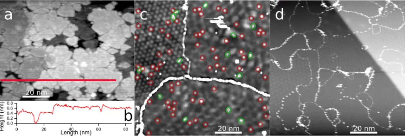
(ML) of gold, is deposited onto the clean SiC substrate at RT (forming three-dimensional islands, not shown) and the sample is then annealed five minutes at an intermediate temperature of 1 050◦C (see Fig.1(a)), the lowest temperature needed to syn-thesize graphene [38]. At this point, the graphenization is not complete and one can see trenches between domains which can be seen in the line profile of Fig. 1(b). Those trenches disap-pear during the step 2 graphene synthesis and are the source of GB [39,40].
Second step (step 2 in the following), around one ML of Au is deposited at RT once more. This second Au ML fol-lows also a Volmer–Weber (VW) growth mode on graphene at RT [41, 42]. Then, the sample is annealed at three increas-ing temperatures : 1 100◦C, 1 150◦C and 1 200◦C, 5 minutes
each. Fig. 1(c) shows the surface after (step 2) and exhibits three graphene domains separated by rotational GB. Note that the bulk Au melting temperature is 1 064◦C (even lower for nanoparticles of 1-2 nm) and we can suppose that Au atoms are completely removed from the surface after (step 2) because of evaporation, or diffusion into the bulk [43]. We get FD (cir-cled in red) with a density n around 7 · 1011cm−2. As a FD is composed of 24 atoms, we can also say that ∼ 0.5 % of the atoms are part of FD. The defect-defect first neighbor mean distance is equal to 5.4 ± 2.3 nm (the minimum distance is the size of an isolated FD, i.e. around 2 nm). This result is con-sistent with a Poisson distribution where the nearest neighbor mean distance is 1/(2√n) = 6 nm. This shows that FD posi-tions are random. In Fig.1(c) one can see that larger GBL such as double FD (circled in green) are very scarce with a density around 1011cm−2. Single FD are by far prevailing. This result
is consistent with the fact that bigger GBL are less energeti-cally favored than FD [9]. Similar double FD have already been observed and some of them (with a non-conserved number of atoms) have been called conjoined-twin defect [23]. The three graphene domains exhibit Moir´e Patterns (MP) with different periodicity (mainly related to the twist angle between the two first graphene layers) and the amounts of FD are nearly equal on each one. On one side, this indicates a homogeneous distri-bution of FD all over the surface independently of the relative orientation of the underlying GL. On the other side, this shows that FD are not surrounded by the same atomic environment, and consequently, could have different mechanical and elec-tronic properties. Effectively: i) FD belonging to a same grain are more or less in interaction laterally with each other’s (and
the surrounding GB) and these interactions could induce inho-mogeneous stresses, which have a great importance concerning local mechanical properties [44]; ii) FD seem to be randomly distributed, thus their electronic properties should also depend on their positions relatively to the underlying layer. A point which is discussed below in relation with local electronic spec-troscopy.
Despite the fact that after this synthesis, either by STM or Auger electron spectroscopy we did not find any trace of Au, we cannot exclude the formation of gold carbides or silicides during the high temperature graphene synthesis. Effectively, AuC complexes have already been observed by TEM [45] and previous calculations [46] have shown that Au-C binding en-ergy could be around 0.5 eV higher than the cohesive enen-ergy of bulk Au (3.81 eV). Moreover, we can suppose that during annealing around 1 100◦C, as deposited Au form small liquid droplets before evaporation and constitute temporary sources for Au atoms/clusters diffusion on the surface, which could also form AuSi complexes.
3.2. Discussion about the importance of each step
Starting from the cleaning procedure, all the parameters in this double step process seem to be crucial. For example, we carried out (steps 1 & 2) without Au deposition and ended up with no FD. This means that Au (especially when deposited during (step 2)) plays a key role in the formation of the FD as catalyst. But proto-graphene is also essential.
3.2.1. Synthesis without proto-graphene
If (step 1) is not carried out, i.e. only one Au ML is de-posited on the clean SiC substrate and the sample is then heated gradually until 1 200◦C, it exhibits no FD as shown on Fig.1(d). Effectively, Au melting temperature being lower than 1 100◦C,
we can assume that most of the Au evaporates from the sur-face before it can create defects. Thus, this case is similar to the usual FLG synthesis without Au and our results pre-sented in Fig.1(d) are comparable to previously obtained re-sults [7, 47]. If we compare Fig.s 1(c) and (d), we remark that without (step 1) the final typical domain size is around five times smaller and the sample exhibits a high density of GB. This is also explained by the proto-graphene which, once created, could reduce the area available for new graphene nu-cleation sites during the (step 2) synthesis performed at higher temperature [48,49] and so, could increase the final grain size by limiting the proliferation of graphene flake boundaries. 3.2.2. Proto-graphene as a template for gold anchoring
The first very important point to notice is that after (step 1) graphene is not flat. As shown in Fig.1(a,b), (step 1) is not suf-ficient to create extended graphene domains and the surface is rather similar to graphene obtained on various SiC reconstruc-tions [50]. The large atomic roughness in Fig.1(b) indicates the presence of small islands or clusters of undefined species (Au, C, Si or their combination). We think that those areas are one way toward FD synthesis, as they induce locally im-portant strain in the graphene, that increases the elastic energy.
Figure 1: (a) STM image of proto-graphene on SiC(0001) synthesized after (step 1), i.e. : one Au monolayer deposition at room temperature and a 5 minute synthesis at 1 050◦C (100×74 nm2). (b) Topography along the red line showing the trenches between domains. (c) STM image of three domains of few layer
graphene obtained after (step 1) followed by (step 2), i.e. : a second Au deposition and three successive 5 minute synthesis at 1 100◦C, 1 150◦C and 1 200◦C. On
each of the domains, one have circled in red the flower defects. Bigger grain boundary loops are circled in green (100×100 nm2).(d) STM image of several domains of few layer graphene obtained without (step 1), i.e. : one Au monolayer deposition at room temperature and a 15 minute direct synthesis at 1 200◦C (100×100 nm2). For all the images V=1 V, I=50 pA.
During (step 2), this energy will be released locally and conse-quently may promote a reorganization favorable to the FD. Note also that after (step 1), graphene island borders are connected to the SiC substrate which induces also a residual stress inside islands [39]. So, we argue that there are two main places where (step 2)’s Au would catalyze defects more easily : the small strained area in the graphene flakes and the graphene borders. 3.2.3. Gold as catalyst for the flower defects formation
Au on graphene at RT follows a VW growth mode but the Au island density depends strongly on the graphene defect den-sity such as vacancies, graphene borders and GB [42,51]. All those defects are nucleation areas for island growth [52]. This means that proto-graphene, which exhibits a very high defect density, acts as a perfect template in order to obtain a high den-sity of Au islands during (step 2). We think that it is this asso-ciation which is the driving force for FD formation. We argue that Au islands of nanometer size trapped in the proto-graphene defects modify locally the formation/relaxation of graphene and the healing processes during (step 2). One consequence is the generation of small domains isolated from the rest by GBL such as FD or conjoined-twin defects. Containment of small areas within the rest of the environment has already been observed by TEM [12] and a bulge nucleation mechanism has been pro-posed which has great similarities with our hypothesis. This could be confirmed by molecular dynamic simulations of GB migration [26,29,53] in presence of Au islands.
3.3. Comparisons with bismuth and platinum
(Step 2) is carried out at high temperature (around 1 150◦C)
and the stability of Au islands during this step is the key point to increase the FD density. If islands evaporate before the car-bon disclinations interact with each other under or at the island edges in order to form GBL, there will be no increase of FD density and no gain relatively to a situation without Au. On the contrary, if Au islands do not evaporate (as observed in the
first two annealing at 1 100◦C and 1 150◦C, not shown), there
could be defects under these islands, but they will obviously be invisible to STM. Since the Au melting temperature is lower than the second graphene synthesis temperature, it is the Au is-land size, and therefore their lifetime before total evaporation (which is related to the sublimation rate at this temperature) that controls two things. On the one hand, getting FD, and, on the other hand, removing all the residual Au islands or atoms which could modified the intrinsic flowered-graphene proper-ties. An indirect proof of the importance of the metal melt-ing temperature and the quantity of deposited atoms in (step 2) is to compare our results with those obtained with two other elements which have very different bulk melting temperatures (BMT) : platinum (Pt) and bismuth (Bi) with respective BMT of 1 380◦C and 271◦C, i.e. respectively above and below the (step
2) synthesis temperature. We used Pt instead of Au in (step 1 & 2) and, excepted a lot of residual big Pt islands, we didn’t obtain any observable FD. Nevertheless, we cannot exclude the possibility that FD are located below those islands. Concerning Bi, we recall below that previous experiments [24] realized on the Si-rich face have also generated a great flower-like density, around 1012cm−2, but associated with a nearly equal amount of
undefined point defects. For Bi on SiC(0001) [24], (step 1) was not performed and (step 2) was repeated several times with two major differences compared to our experiments : a larger Bi thickness and a higher temperature, 1 350◦C. The consequence was a low amount of potential sites for the nucleation of Bi is-lands which could have catalyzed FD formation. Associated with its very low BMT (and so a very high sublimation rate at those temperatures), this explains why (step 2) has to be re-peated several times before reaching a significant density of FD. Moreover, it must be pointed out that the graphene growth on the Si-rich surface is intrinsically not a good candidate to obtain selectively a high density of FD. The growth modes of graphene on the Si-rich and C-rich faces are very different. On the former, it is a rolling-carpet mechanism starting at the SiC step edges, 4
while on the latter, it is a nucleation growth mode from the SiC terraces. It follows that on the Si-rich face, the first successive graphene planes (included the buffer layer) are in epitaxial rela-tionship with the substrate and have very few grain boundaries, whereas on the C-rich face, the graphene planes are rotated rel-atively to each other, thus forming both MP and having a high density of grain boundaries constituted mainly by disclinations and vacancies. Since flower defects are obtained from the orga-nized clustering of disclinations, it is clear that the more discli-nations there are, the greater the density of flower defects will be. However, this is directly related to the density of point de-fects present during graphene synthesis. It is therefore expected to be more ”difficult” to obtain a high density of flower defects on the Si side compared to the C side. This is indeed what is observed with bismuth assisted FD formation on the Si-rich face [24] or the necessity to synthetize the graphene at high temperature [23] in order to obtain a high density of defects, among which a certain amount of FD.
3.4. First-principles calculation of FD formation energy Once we have understood that after (step 1) a great amount of potential FD sites (among other extended defects) have been created along graphene flake borders and stressed regions, we theoretically investigate the role of Au during FD formation. So we calculate the FD formation energy, Ef, by first-principles
calculations (see Methods2.3). We define Ef as
Ef = E(FD + n.Au) − E(GR + n.Au) (2)
where the first right-hand side term is the total energy of the FD in contact with n Au atoms, and the second one is the to-tal energy of the corresponding pristine graphene structure also with n Au. To emphasize the catalytic role played by gold to form FD, Ef is calculated for n Au atoms (n=1 to 12) located
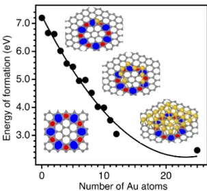
in direct contact with the defects. More precisely, our calcu-lations show that the most stable position for one Au atom is in bridge between the pentagonal and heptagonal rings. There-fore, different configurations will be investigated further when the n Au atoms are close or far from each other on these specific sites. First of all, it can be seen that the formation energy with-out Au atom is equal to 7.20 eV which is in agreement with previous results [9,26]. Interestingly, our calculations show clearly that Ef decreases significantly in presence of Au atoms
to reach 3.05 eV for n = 12. As seen in Fig.2, the decrease is not continuous. Indeed, it depends on the way Au atoms inter-act locally with the topological defects present in the graphene. To go further, a flake of 25 Au atoms fully covering the FD is considered. They are forming a closed-packed structure which can be assimilated to the contact zone characterizing the inter-action of a (111) facet of a nanoparticle with the FD. By doing so, the decrease in Ef is even more pronounced and achieves a
value of about 2.5 eV. Consequently, those results clearly show that Au promotes formation of FD.
This catalytic role of Au is achieved through its strong in-teraction with the topological defects present in graphene. To highlight this mechanism, the adsorption energy (Eads) of an Au
atom on a SW defect is calculated and compared with pristine
Figure 2: Flower defect formation energy as a function of the number of gold atoms. Insets : relaxed atomic positions of a flower defect without (left) and with 1, 8 and 25 Au atoms (left). Carbon atoms are in black and Au atoms are in yellow. Pentagonal and heptagonal rings are filled in red and blue, respectively.
graphene (see Methods 2.3). The adsorption of Au atoms on graphene has been studied on several graphene sites, including the highly symmetric sites (top, bridge and hollow). According to our calculations, the most stable positon for the Au adatom is on top of a C atom for an adhesion energy of about -0.51 eV in line with data from the literature [54,55,56]. In the presence of the SW defect, Eads is equal to -2.51 eV revealing that the
interaction of Au atoms with topological defects is very strong which suggests that Au atoms can play a crucial role for the formation of FD.
It is interesting to note that similar calculations have shown that the energy barrier for the elimination of SW defects (around 5 eV) [57] can be drastically decreased by adsorbed transition metal atoms [58,59]. In the present work, we were also able to highlight this effect. We performed the same kind of study done for FD with a SW defect. In a similar way, we observe a strong reduction of the formation energy in the presence of Au atoms. Indeed, the formation energy of a SW defect is 5.3 eV accord-ing to our calculations. In this particular case, the Au atom occupies the bridge position and tends to strongly decrease the defect formation energy by about 25% to reach 3.92 eV. Start-ing from 3 atoms, the Ef value tends to stabilize around 3 eV.
Note that once 5|7 pairs or SW defects are formed, by an un-known out of equilibrium atomic process during the graphene formation, they are stable in the temperature range that we use. So, our experimental and theoretical results show that Au, act-ing as a catalyst, decreases FD formation energy.
Finally, we can say that two main mechanisms act to form a high density of FD. On one hand, Au (and eventually Bi, Pt and other species) catalyzes FD and flower-like defects be-cause it decreases the SW and loops formation energy. And, on the other hand, (step 1) increases the number of local stressed areas induced by trenches and graphene defects in the proto-graphene, which thus prepares a lot of potential sites for Au an-choring during (step-2) and so favoring the formation of
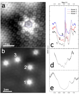
point-Figure 3: (a) Scanning tunelling microscopy image of a flower defect with the qualitative atomic model superimposed over it (4×4 nm2, V=1 V, I=100 pA).(b) Topographic image of 5 other flower defects (15×15 nm2, V=220 mV, I= 1 nA).(c) dI/dV spectra taken on three of the defects in (b). Offsets have been added for clarity. (d, e) dI/dV spectra taken on FD belonging to two other grains.
like defects.
3.5. STM/STS characterization of flower defects 3.5.1. Topography and spectroscopy at high energy
The topography of a FD is reported in more details in Fig.3(a) and its appearance is similar to that previously reported [9,24] (an atomic model is superimposed to the experimental image). The defect appears as a grey center located on the seven central hexagons, surrounded by a white crown located on the joined 5|7 pairs, prolonged by six lobes emerging from the heptagons. Far from the defect (bottom left part), one can see the hon-eycomb lattice of graphene and closer to it one can see the (
√ 3 ×
√
3)R30◦ electronic pattern due to electrons scattering by the defect [17]. Note that all apparent heights (and so the grey scale from 0 to 1.1 Å) are not related to atomic corru-gation but mostly to local variations of the electronic densi-ties. Fig.3(b) shows a STM image of five FD belonging to the same graphene domain exhibiting a unique moir´e pattern (MP). Whatever the MP, we never noticed a clear crystallographic re-lationship between FD location and the apparent moir´e period-icity. It means that, on one side, the underlying GL plays no role in the FD location, and, on the other side, that the seven rotated central hexagons are not exactly above the same under-lying carbon stacking. Fig.3(c) shows three differential con-ductance (dI/dV) spectra taken on three of the FD in Fig.3(b). There are two broads peaks around -0.9 eV and 0.8 eV and a series of fine peaks at positive energies between 0.1-0.5 eV, just
above the pseudo-gap [32] centered at EF (see also Fig.4(e)).
These features in the eV range are consistent with previous re-ports [4,9,22,23,24] but our measurements display a better re-solved fine structure. More precisely, FD electronic fingerprint is usually observed as a broad resonant peak in the graphene empty states located around 300 to 400 meV above the Dirac Point (DP). This localized resonance is characteristic of iso-lated SW defects [60,61] and similar to van Hove singulari-ties which emerge in one-dimensional ordered GB [7,62,63]. Note that FD which are within the same graphene grain, as in Fig.3(b), exhibit very similar spectra (this has been systemat-ically observed on several domains) : same peaks at the same energies with slightly different intensities. The number and en-ergy position of these fine FD peaks centered around 0.25 eV in Fig. 3(c) strongly depend on the scanned graphene grain which suggests that these states are sensitive to the surround-ing atomic arrangement (see also spectra reported in Fig.3(d,e) obtained on two different grains, but with a lower resolution), but they are always in the empty states. Correlatively, the map-ping of those states is very sensitive to the orientation of un-derlying GL. Those two observations are a strong indication that FD may interact not only with their lateral atomic environ-ment, but also they couple with the underlying surface. This coupling could explain the multiple peaks structure observed between 0.1-0.5 eV and not predicted by first-principles calcu-lations [9] but presenting great similarities with previous STS measurements performed on flat regular GB on SiC(0001) [7]. Despite the large energy range we have experimentally explored ±1.5 eV, there is no localized state in the filled states.
3.5.2. Mapping of low energy states
Zooming the low energy range, i.e. few tens of meV, it is intriguing to see that spectra taken on the different lobes (hep-tagons) of a FD, see Fig.4(a), have several clear peaks inside the gap and rather close to EF, see Fig. 4(e). We recall that
most of the effective electron tunelling in graphene is inelastic electron tunelling mediated by phonons [64] and that a typical STS spectrum on pristine graphene exhibits a gap-like feature (see also Fig.3(c)) between -64 mV and+64 mV (which we confirmed using d2I/dV2measurements). Through an extended
study of several defects at different positions on the sample and with different tips we always noticed that diametrically opposed lobes have very similar spectra. Differential conductance maps obtained from grid spectroscopy at different energies are re-ported in Fig.4(b-d). That shows that opposing lobes ”light up” at the same energy. We also notice that two or four lobes ”light up” at the same time but never all six of them. This is surprising in the sense that it breaks the obvious six-fold sym-metry that one could expect from the defect. Two possibilities are open. On one hand, the surrounding electronic modulation (induced by defects proximity, anisotropic strain, etc.) could be coupled to those electronic states and thus breaks the six-fold symmetry. On the other hand, FD belonging to the same grain are surrounded by the same MP induced by the twist an-gle of the graphene bilayer. It follows that the periodic tran-sition from AB to AA local stackings of the graphene bilayer are locally disturbed by each FD. Thus, because of the FD ran-6
Figure 4: (a) Topographic image of another flower defect (3.5×3.5 nm2, V=500 mV, I=400 pA) and differential conductance intensity maps taken from grid
spectroscopy at (b) 63 mV (c) 4 mV and (d) -20 mV on the same defect. (e) dI/dV spectra taken on (a) with a set point at 500 mV and 400 pA. The black curve is taken on the graphene (white ’+’ in (a)) and shows the phonon gap. The red and blue curves are taken on two different lobes of the defect (red and blue ’+’s in (a)) and show both the phonon gap and several peaks inside the gap.
domness location, one should expect variable electronic states from FD to FD. For example, if a flower is in an AA stacking bilayer, its symmetry is not broken, and we should observe a 6-fold symmetry. In case of a Bernal-stacked bilayer we should observe a 3-fold symmetry, as already suggested [9]. Note that a similar symmetry breaking processes induced by a defect in a graphene bilayer has previously been invoked in order to ex-plain the shape of FD [19]. Due to randomness of FD posi-tions in a same grain (and also the same MP), they have not the same underlying stacking (except for the AA or AB stack-ing which are rather rare), which also breaks their symmetry. This second possibility is the more likely of the two because it is coherent with the spectroscopy done at high energy where all FD residing on the same MP exhibit the same spectrum what-ever their proximity with other defects. We can not explain the physical origin of those in-gap states (these states have already been measured in a very different atomic configurations, i.e. along graphene nanoribbons on Au(111) [65] and along ridges on SiC(0001) [66])), but the FD special topology coupled to the interaction with the underlying graphene could induce new states due to electronic confinement. Recent calculations on cir-cular quantum dots in twisted bilayer graphene are certainly a hint to understand those states [67].
Conclusion
In summary, scanning tunelling microscopy and spectroscopy studies of flower defect formation catalyzed by gold on few-layer graphene on SiC(0001) have been presented. A very high density of flower defects is obtained thanks to a two-steps pro-cess. A proto-graphene layer creates a template for anchoring gold clusters which promotes the formation of those quasi-point like topological defects during the second step. First-principles calculations provide clear evidence for a drastic decrease of
their formation energy with gold. These flowers exhibit lo-calized electronic states all over the defect at high energy, and interestingly low energy states localized asymmetrically on the heptagons breaking the apparent flower defect 6-fold symmetry. The complex formation of those defects during the graphene synthesis on SiC could be studied by molecular dynamic simu-lations. The unknown in-gap states deserve future experiments and theoretical developments.
Acknowledgments
The authors received no specific funding for this work.
References
[1] Z. Wu, Z. Ni, Spectroscopic investigation of defects in two-dimensional materials, Nanophot. 6 (6) (2017) 1219–1237 (Mar. 2017). doi:10. 1515/nanoph-2016-0151.
[2] F. Joucken, Y. Tison, J. Lagoute, J. Dumont, D. Cabosart, B. Zheng, V. Repain, C. Chacon, Y. Girard, A. R. Botello-M´endez, S. Rousset, R. Sporken, J.-C. Charlier, L. Henrard, Localized state and charge trans-fer in nitrogen-doped graphene, Phys. Rev. B 85 (16) (2012) 161408 (Apr. 2012).doi:10.1103/PhysRevB.85.161408.
[3] L. Zhao, R. He, K. T. Rim, T. Schiros, K. S. Kim, H. Zhou, C. Guti´errez, S. P. Chockalingam, C. J. Arguello, L. P´alov´a, D. Nordlund, M. S. Hy-bertsen, D. R. Reichman, T. F. Heinz, P. Kim, A. Pinczuk, G. W. Flynn, A. N. Pasupathy, Visualizing Individual Nitrogen Dopants in Monolayer Graphene, Science 333 (6045) (2011) 999 (Aug. 2011).doi:10.1126/ science.1208759.
[4] L. Zhao, M. Levendorf, S. Goncher, T. Schiros, L. P´alov´a, A. Zabet-Khosousi, K. T. Rim, C. Guti´errez, D. Nordlund, C. Jaye, M. Hy-bertsen, D. Reichman, G. W. Flynn, J. Park, A. N. Pasupathy, Local Atomic and Electronic Structure of Boron Chemical Doping in Mono-layer Graphene, Nano Lett. 13 (10) (2013) 4659–4665 (Oct. 2013).doi: 10.1021/nl401781d.
[5] F. Joucken, L. Henrard, J. Lagoute, Electronic properties of chemically doped graphene, Phys. Rev. Materials 3 (11) (2019) 110301 (Nov. 2019).
[6] F. Ducastelle, Electronic structure of vacancy resonant states in graphene: A critical review of the single-vacancy case, Phys. Rev. B 88 (7) (2013) 075413 (Aug. 2013).doi:10.1103/PhysRevB.88.075413.
[7] Y. Tison, J. Lagoute, V. Repain, C. Chacon, Y. Girard, F. Joucken, R. Sporken, F. Gargiulo, O. V. Yazyev, S. Rousset, Grain Boundaries in Graphene on SiC(0001) Substrate, Nano Lett. 14 (11) (2014) 6382–6386 (Nov. 2014).doi:10.1021/nl502854w.
[8] G. Yang, L. Li, W. B. Lee, M. C. Ng, Structure of graphene and its disorders: A review, Science and Technology of Advanced Materials 19 (1) (2018) 613–648 (Dec. 2018). doi:10.1080/14686996.2018. 1494493.
[9] E. Cockayne, G. M. Rutter, N. P. Guisinger, J. N. Crain, P. N. First, J. A. Stroscio, Grain boundary loops in graphene, Phys. Rev. B 83 (19) (2011) 195425 (May 2011).doi:10.1103/PhysRevB.83.195425.
[10] L. Linhart, J. Burgd¨orfer, F. Libisch, Accurate modeling of defects in graphene transport calculations, Phys. Rev. B 97 (3) (2018) 035430 (Jan. 2018).doi:10.1103/PhysRevB.97.035430.
[11] D. Kang, C. Zhang, H. Li, Spin Transport in Zigzag Graphene Nanorib-bon with a Flower Defect, J Supercond Nov Magn 32 (12) (2019) 3927– 3931 (Dec. 2019).doi:10.1007/s10948-019-05180-y.
[12] A. Cresti, J. Carrete, H. Okuno, T. Wang, G. K. H. Madsen, N. Mingo, P. Pochet, Growth, charge and thermal transport of flowered graphene, Carbon 161 (2020) 259–268 (May 2020). doi:10.1016/j.carbon. 2020.01.040.
[13] Y. Chen, M.-C. Li, Q.-M. Wang, G.-S. Wang, X. Wei, G.-F. Song, X.-M. Kong, Y. Xu, Y. Liu, Structure and electronic properties of closed-ring defects in epitaxial graphene, Mater. Res. Express 7 (5) (2020) 055602 (May 2020).doi:10.1088/2053-1591/ab8ee6.
[14] T. Bj¨orkman, S. Kurasch, O. Lehtinen, J. Kotakoski, O. V. Yazyev, A. Sri-vastava, V. Skakalova, J. H. Smet, U. Kaiser, A. V. Krasheninnikov, De-fects in bilayer silica and graphene: Common trends in diverse hexag-onal two-dimensihexag-onal systems, Sci Rep 3 (1) (2013) 3482 (Dec. 2013).
doi:10.1038/srep03482.
[15] M. Pivetta, M.-C. Bl¨um, F. Patthey, W.-D. Schneider, Two-Dimensional Tiling by Rubrene Molecules Self-Assembled in Supramolecular Pen-tagons, Hexagons, and Heptagons on a Au(111) Surface, Angew. Chem. Int. Ed. 47 (6) (2008) 1076–1079 (2008). doi:10.1002/anie. 200704479.
[16] B. An, S. Fukuyama, K. Yokogawa, Graphitization of 6H–SiC(000\bar1) Surface by Scanning Tunneling Microscopy, Jpn. J. Appl. Phys. 41 (Part 1, No. 7B) (2002) 4890–4893 (Jul. 2002). doi:10.1143/JJAP.41. 4890.
[17] G. M. Rutter, J. N. Crain, N. P. Guisinger, T. Li, P. N. First, J. A. Stroscio, Scattering and Interference in Epitaxial Graphene, Science 317 (5835) (2007) 219–222 (Jul. 2007).doi:10.1126/science.1142882. [18] N. P. Guisinger, G. M. Rutter, J. N. Crain, C. Heiliger, P. N. First,
J. A. Stroscio, Atomic-scale investigation of graphene formation on 6H-SiC(0001), J. Vac. Sci. Technol. A 26 (4) (2008) 932 (Jul. 2008). doi: 10.1116/1.2900661.
[19] L. Simon, C. Bena, F. Vonau, D. Aubel, H. Nasrallah, M. Habar, J. C. Peruchetti, Symmetry of standing waves generated by a point defect in epitaxial graphene, Eur. Phys. J. B 69 (3) (2009) 351–355 (Jun. 2009).
doi:10.1140/epjb/e2009-00142-3.
[20] H. J. Park, V. Sk´akalov´a, J. Meyer, D. S. Lee, T. Iwasaki, C. Bumby, U. Kaiser, S. Roth, Growth and properties of chemically modified graphene, Phys. Stat. Sol. 247 (11-12) (2010) 2915–2919 (2010). doi: 10.1002/pssb.201000818.
[21] H. I. Rasool, E. B. Song, M. Mecklenburg, B. C. Regan, K. L. Wang, B. H. Weiller, J. K. Gimzewski, Atomic-Scale Characterization of Graphene Grown on Copper (100) Single Crystals, J. Am. Chem. Soc. 133 (32) (2011) 12536–12543 (Aug. 2011).doi:10.1021/ja200245p. [22] H. Yan, C.-C. Liu, K.-K. Bai, X. Wang, M. Liu, W. Yan, L. Meng,
Y. Zhang, Z. Liu, R.-f. Dou, J.-C. Nie, Y. Yao, L. He, Electronic struc-tures of graphene layers on a metal foil: The effect of atomic-scale defects, App. Phys. Lett. 103 (14) (2013) 143120 (Oct. 2013). doi: 10.1063/1.4824206.
[23] Y. Cui, H. Zhang, W. Chen, Z. Yang, Q. Cai, Structural Evolution of Flower Defects and Effects on the Electronic Structures of Epitaxial Graphene, J. Phys. Chem. C 121 (28) (2017) 15282–15287 (Jul. 2017).
doi:10.1021/acs.jpcc.7b04693.
[24] T. Hu, D. Ma, Q. Fang, P. Zhang, X. Liu, R. Wei, Y. Pan, K. Xu, F. Ma,
Bismuth mediated defect engineering of epitaxial graphene on SiC(0001), Carbon 146 (2019) 313–319 (May 2019). doi:10.1016/j.carbon. 2019.02.014.
[25] J. C. Meyer, C. Kisielowski, R. Erni, M. D. Rossell, M. F. Crommie, A. Zettl, Direct Imaging of Lattice Atoms and Topological Defects in Graphene Membranes, Nano Lett. 8 (11) (2008) 3582–3586 (Nov. 2008).
doi:10.1021/nl801386m.
[26] S. Kurasch, J. Kotakoski, O. Lehtinen, V. Sk´akalov´a, J. Smet, C. E. Krill, A. V. Krasheninnikov, U. Kaiser, Atom-by-Atom Observation of Grain Boundary Migration in Graphene, Nano Lett. 12 (6) (2012) 3168–3173 (Jun. 2012).doi:10.1021/nl301141g.
[27] J. Kotakoski, J. C. Meyer, Mechanical properties of polycrystalline graphene based on a realistic atomistic model, Phys. Rev. B 85 (19) (2012) 195447 (May 2012).doi:10.1103/PhysRevB.85.195447. [28] E. Cockayne, Graphing and grafting graphene: Classifying finite
topo-logical defects, Phys. Rev. B 85 (12) (2012) 125409 (Mar. 2012). doi: 10.1103/PhysRevB.85.125409.
[29] J. Zhuang, R. Zhao, J. Dong, T. Yan, F. Ding, Evolution of domains and grain boundaries in graphene: A kinetic Monte Carlo simulation, Phys. Chem. Chem. Phys. 18 (4) (2016) 2932–2939 (Jan. 2016). doi: 10.1039/C5CP07142A.
[30] H. Terrones, R. Lv, M. Terrones, M. S. Dresselhaus, The role of defects and doping in 2D graphene sheets and 1D nanoribbons, Rep. Prog. Phys. 75 (6) (2012) 062501 (May 2012). doi:10.1088/0034-4885/75/6/ 062501.
[31] S. Karoui, H. Amara, C. Bichara, F. Ducastelle, Nickel-Assisted Healing of Defective Graphene, ACS Nano 4 (10) (2010) 6114–6120 (Oct. 2010).
doi:10.1021/nn101822s.
[32] Y. Zhang, V. W. Brar, F. Wang, C. Girit, Y. Yayon, M. Panlasigui, A. Zettl, M. F. Crommie, Giant phonon-induced conductance in scanning tun-nelling spectroscopy of gate-tunable graphene, Nature Phys 4 (8) (2008) 627–630 (Aug. 2008).doi:10.1038/nphys1022.
[33] P. Giannozzi, S. Baroni, N. Bonini, M. Calandra, R. Car, C. Cavazzoni, D. Ceresoli, G. L. Chiarotti, M. Cococcioni, I. Dabo, A. D. Corso, S. de Gironcoli, S. Fabris, G. Fratesi, R. Gebauer, U. Gerstmann, C. Gougous-sis, A. Kokalj, M. Lazzeri, L. Martin-Samos, N. Marzari, F. Mauri, R. Mazzarello, S. Paolini, A. Pasquarello, L. Paulatto, C. Sbraccia, S. Scandolo, G. Sclauzero, A. P. Seitsonen, A. Smogunov, P. Umari, R. M. Wentzcovitch, QUANTUM ESPRESSO: A modular and open-source software project for quantum simulations of materials, J. Phys.: Condens. Matter 21 (39) (2009) 395502 (Sep. 2009). doi:10.1088/ 0953-8984/21/39/395502.
[34] P. E. Bl¨ochl, Projector augmented-wave method, Phys. Rev. B 50 (24) (1994) 17953–17979 (Dec. 1994). doi:10.1103/PhysRevB.50. 17953.
[35] J. P. Perdew, K. Burke, M. Ernzerhof, Generalized gradient approxima-tion made simple, Phys. Rev. Lett. 77 (18) (1996) 3865–3868 (Oct. 1996).
doi:10.1103/PhysRevLett.77.3865.
[36] N. Mishra, J. Boeckl, N. Motta, F. Iacopi, Graphene growth on silicon carbide: A review, Phys. Stat. Sol. 213 (9) (2016) 2277–2289 (2016).
doi:10.1002/pssa.201600091.
[37] J. Hass, F. Varchon, J. E. Mill´an-Otoya, M. Sprinkle, N. Sharma, W. A. de Heer, C. Berger, P. N. First, L. Magaud, E. H. Conrad, Why Multilayer Graphene on 4H-SiC(000-1) Behaves Like a Single Sheet of Graphene, Phys. Rev. Lett. 100 (12) (2008) 125504 (Mar. 2008). doi:10.1103/ PhysRevLett.100.125504.
[38] I. Forbeaux, J.-M. Themlin, J.-M. Debever, High-temperature graphiti-zation of the 6H-SiC (0001) face, Surf. Sci. 442 (1) (1999) 9–18 (Nov. 1999).doi:10.1016/S0039-6028(99)00891-2.
[39] A. Tiberj, J.-R. Huntzinger, J. Camassel, F. Hiebel, A. Mahmood, P. Mal-let, C. Naud, J.-Y. Veuillen, Multiscale investigation of graphene layers on 6H-SiC(000-1), Nanoscale Res Lett 6 (1) (2011) 171 (Dec. 2011).
doi:10.1186/1556-276X-6-171.
[40] L. P. Bir´o, P. Lambin, Grain boundaries in graphene grown by chemical vapor deposition, New J. Phys. 15 (3) (2013) 035024 (Mar. 2013).doi: 10.1088/1367-2630/15/3/035024.
[41] L. Liu, Z. Chen, L. Wang, E. Polyakova (Stolyarova), T. Taniguchi, K. Watanabe, J. Hone, G. W. Flynn, L. E. Brus, Slow Gold Adatom Di ffu-sion on Graphene: Effect of Silicon Dioxide and Hexagonal Boron Nitride Substrates, J. Phys. Chem. B 117 (16) (2013) 4305–4312 (Apr. 2013).
doi:10.1021/jp305521g.
[42] X. Liu, C.-Z. Wang, M. Hupalo, H.-Q. Lin, K.-M. Ho, M. Tringides, Metals on Graphene: Interactions, Growth Morphology, and Thermal Stability, Crystals 3 (1) (2013) 79–111 (Jan. 2013). doi:10.3390/ cryst3010079.
[43] M.-Y. Li, Q. Zhang, P. Pandey, M. Sui, E.-S. Kim, J. Lee, From the Au nano-clusters to the nanoparticles on 4H-SiC (0001), Sci. Rep. 5 (1) (Nov. 2015).doi:10.1038/srep13954.
[44] J. Zhang, J. Zhao, Mechanical properties of bilayer graphene with twist and grain boundaries, J. App. Phys. 113 (4) (2013) 043514 (Jan. 2013).
doi:10.1063/1.4789594.
[45] B. Westenfelder, J. Biskupek, J. C. Meyer, S. Kurasch, X. Lin, F. Scholz, A. Gross, U. Kaiser, Bottom-up formation of robust gold carbide, Sci Rep 5 (1) (2015) 1–6 (Mar. 2015).doi:10.1038/srep08891.
[46] S. Stolbov, M. Alc´antara Ortigoza, Gold-doped graphene: A highly stable and active electrocatalysts for the oxygen reduction reaction, J. Chem. Phys. 142 (15) (2015) 154703 (Apr. 2015).doi:10.1063/1.4917468. [47] F. Varchon, P. Mallet, L. Magaud, J.-Y. Veuillen, Rotational disorder in
few-layer graphene films on 6 H - Si C ( 000 - 1 ) : A scanning tunneling microscopy study, Phys. Rev. B 77 (16) (2008) 165415 (Apr. 2008).doi: 10.1103/PhysRevB.77.165415.
[48] W. Norimatsu, M. Kusunoki, Growth of graphene from SiC{0001} sur-faces and its mechanisms, Semicond. Sci. Technol. 29 (6) (2014) 064009 (Jun. 2014).doi:10.1088/0268-1242/29/6/064009.
[49] L. B. Biedermann, M. L. Bolen, M. A. Capano, D. Zemlyanov, R. G. Reifenberger, Insights into few-layer epitaxial graphene growth on 4H-SiC(000-1) substrates from STM studies, Phys. Rev. B 79 (12) (2009) 125411 (Mar. 2009).doi:10.1103/PhysRevB.79.125411.
[50] F. Hiebel, P. Mallet, F. Varchon, L. Magaud, J.-Y. Veuillen, Graphene-substrate interaction on 6 H -SiC ( 000-1 ) : A scanning tunneling microscopy study, Phys. Rev. B 78 (15) (2008) 153412 (Oct. 2008).
doi:10.1103/PhysRevB.78.153412.
[51] A. Pulido, M. Boronat, A. Corma, Theoretical investigation of gold clus-ters supported on graphene sheets, New J. Chem. 35 (10) (2011) 2153– 2161 (2011).doi:10.1039/C1NJ20215D.
[52] T. Irawan, I. Barke, H. H¨ovel, Size-dependent morphology of gold clus-ters grown on nanostructured graphite, Appl. Phys. A 80 (5) (2005) 929– 935 (Feb. 2005).doi:10.1007/s00339-004-3118-8.
[53] E. Annevelink, E. Ertekin, H. T. Johnson, Grain boundary structure and migration in graphene via the displacement shift complete lattice, Acta Materialia 166 (2019) 67–74 (Mar. 2019).doi:10.1016/j.actamat. 2018.12.030.
[54] K. T. Chan, J. B. Neaton, M. L. Cohen, First-principles study of metal adatom adsorption on graphene, Phys. Rev. B 77 (23) (2008) 235430 (Jun. 2008).doi:10.1103/PhysRevB.77.235430.
[55] K. Nakada, A. Ishii, Migration of adatom adsorption on graphene us-ing DFT calculation, Solid State Commun. 151 (1) (2011) 13–16 (2011).
doi:10.1016/j.ssc.2010.10.036.
[56] M. Manad´e, F. Vi˜nes, F. Illas, Transition metal adatoms on graphene: A systematic density functional study, Carbon 95 (2015) 525–534 (2015).
doi:10.1016/j.carbon.2015.08.072.
[57] L. Li, S. Reich, J. Robertson, Defect energies of graphite: Density-functional calculations, Phys. Rev. B 72 (18) (2005) 184109 (Nov. 2005).
doi:10.1103/PhysRevB.72.184109.
[58] J.-C. Charlier, H. Amara, P. Lambin, Catalytically Assisted Tip Growth Mechanism for Single-Wall Carbon Nanotubes, ACS Nano 1 (3) (2007) 202–207 (Oct. 2007).doi:10.1021/nn700049q.
[59] W.-W. Wang, J.-S. Dang, J.-J. Zheng, X. Zhao, E. ¯Osawa, S. Na-gase, Metal-promoted restoration of defective graphene, J. Mater. Chem. 22 (32) (2012) 16370–16375 (Jul. 2012).doi:10.1039/C2JM31703F. [60] H. Amara, S. Latil, V. Meunier, P. Lambin, J.-C. Charlier, Scanning
tunneling microscopy fingerprints of point defects in graphene: A the-oretical prediction, Phys. Rev. B 76 (11) (2007) 115423 (Sep. 2007).
doi:10.1103/PhysRevB.76.115423.
[61] A. Lherbier, S. M.-M. Dubois, X. Declerck, S. Roche, Y.-M. Niquet, J.-C. Charlier, Two-Dimensional Graphene with Structural Defects: Elas-tic Mean Free Path, Minimum Conductivity, and Anderson Transition, Phys. Rev. Lett. 106 (4) (2011) 046803 (Jan. 2011). doi:10.1103/ PhysRevLett.106.046803.
[62] O. V. Yazyev, S. G. Louie, Electronic transport in polycrystalline graphene, Nature Mater 9 (10) (2010) 806–809 (Oct. 2010). doi: 10.1038/nmat2830.
[63] A. Luican-Mayer, J. E. Barrios-Vargas, J. T. Falkenberg, G. Aut`es, A. W. Cummings, D. Soriano, G. Li, M. Brandbyge, O. V. Yazyev, S. Roche, E. Y. Andrei, Localized electronic states at grain boundaries on the surface of graphene and graphite, 2D Mater. 3 (3) (2016) 031005 (Aug. 2016).
doi:10.1088/2053-1583/3/3/031005.
[64] J. ˇCervenka, K. van de Ruit, C. F. J. Flipse, Local enhancement of in-elastic tunnelling in epitaxial graphene on SiC(0001), Phys. Stat. Sol. B 247 (11-12) (2010) 2992–2996 (Dec. 2010). doi:10.1002/pssb. 201000167.
[65] C. Tao, L. Jiao, O. V. Yazyev, Y.-C. Chen, J. Feng, X. Zhang, R. B. Ca-paz, J. M. Tour, A. Zettl, S. G. Louie, H. Dai, M. F. Crommie, Spatially resolving edge states of chiral graphene nanoribbons, Nature Phys 7 (8) (2011) 616–620 (Aug. 2011).doi:10.1038/nphys1991.
[66] M. Ridene, J. C. Girard, L. Travers, C. David, A. Ouerghi, STM/STS investigation of edge structure in epitaxial graphene, Surf. Sci. 606 (15) (2012) 1289–1292 (Aug. 2012).doi:10.1016/j.susc.2012.04.006. [67] M. Mirzakhani, F. M. Peeters, M. Zarenia, Circular quantum dots in twisted bilayer graphene, Phys. Rev. B 101 (7) (2020) 075413 (Feb. 2020).doi:10.1103/PhysRevB.101.075413.