HAL Id: tel-01560333
https://tel.archives-ouvertes.fr/tel-01560333
Submitted on 11 Jul 2017
HAL is a multi-disciplinary open access archive for the deposit and dissemination of sci-entific research documents, whether they are pub-lished or not. The documents may come from teaching and research institutions in France or abroad, or from public or private research centers.
L’archive ouverte pluridisciplinaire HAL, est destinée au dépôt et à la diffusion de documents scientifiques de niveau recherche, publiés ou non, émanant des établissements d’enseignement et de recherche français ou étrangers, des laboratoires publics ou privés.
To cite this version:
Sara Gonzalez. Operando Chemistry and Electronic Structure of Electrode/Ferroelectric Interfaces. Materials Science [cond-mat.mtrl-sci]. Université Paris-Saclay; Universität Duisburg-Essen, 2016. En-glish. �NNT : 2016SACLS501�. �tel-01560333�
3
NNT : 2016SACLS501
T
HESE DE DOCTORAT
DE
U
NIVERSITY OF
D
UISBURG
-E
SSEN
ET DE
L’U
NIVERSITE
P
ARIS
-S
ACLAY
PREPAREE A
L’U
NIVERSITE
P
ARIS
-S
UD
E
COLED
OCTORALE N° 564
Physique en Ile-de-France
Spécialité de doctorat : Physique
Par
M
lleSara GONZALEZ
Operando Chemistry and Electronic Structure of Electrode/Ferroelectric
Interfaces
Thèse présentée et soutenue à Duisburg-Essen University, le 30 novembre 2016 :
Composition du Jury :
Dr, Kratzer, Peter Professeur, Faculty of Physics, Universität Duisburg-Essen Président Dr, Jedrecy, Nathalie Professeur, Institut des NanoSciences de Paris Rapporteur Dr, Pintilie, Lucian Professeur, National Institute of Materials Physics Rapporteur Dr, Wende, Heiko Professeur, Faculty of Physics, Universität Duisburg-Essen Examinateur
Dr, Barrett, Nick Docteur, CEA-Saclay Co-directeur de thèse Dr, Schneider, Claus Professeur, PGI-6 Jülich & Universität Duisburg-Essen Co-directeur de thèse
Operando Chemistry and
Electronic Structure of
Electrode/Ferroelectric Interfaces
Von der Fakultät Physik
der Universität Duisburg-Essen
zur Erlangung des Grades
Doktor der Naturwissenschaften
(Dr. rer. nat.)
genehmigte Dissertation
von
Sara Gonzalez
geb. am 11. November 1990 in Paris
Tag der mündlichen Prüfung: 30.11.2016 Tag des Einreichung: 07.10.2016
Jury composition:
Dr, Kratzer, Peter Professor, Faculty of Physics, Universität Duisburg-Essen President Dr, Jedrecy, Nathalie Professor, Institut des NanoSciences de Paris Reviewer Dr, Pintilie, Lucian Professor, National Institute of Materials Physics Reviewer Dr, Wende, Heiko Professor, Faculty of Physics, Universität Duisburg-Essen Examiner
Dr, Barrett, Nick Doctor, CEA-Saclay Thesis co-director Dr, Schneider, Claus Professor, PGI-6 Jülich - Universität Duisburg-Essen Thesis co-director
Acknowledgements
Je tiens tout d’abord à remercier Serge PALACIN, chef de l’ancien Service de Physique Chimie Surfaces et Interfaces, et François DAVIAUD, chef du Service de Physique de l’Etat Condensé du CEA-Saclay pour m’avoir permis de travailler durant trois ans en tant que doc-torante dans ces deux laboratoires.
Je suis très reconnaissante envers Nathalie JEDRECY et Lucian PINTILIE pour avoir accepté la position de rapporteurs de thèse et pour les commentaires très utiles qu’ils ont apportés sur mon travail, ainsi que les autres membres de mon comité de défense de thèse : Peter KRATZER et Heiko WENDE.
J’aimerais ensuite remercier mes co-directeurs de thèse, Nick BARRETT et Claus SCHNEI-DER, qui m’ont accordé leur confiance, dans un contexte où un financement de thèse n’est pas une chose que l’on accorde à la légère. Nick m’a accompagnée au jour le jour. Je le remercie pour tout ce qu’il m’a appris, et pour la très grande charge de travail qu’il a investi pour me permettre de réaliser mon doctorat dans les meilleures conditions. Bien qu’ayant passé moins de temps au quotidien avec Claus SCHNEIDER, celui-ci a toujours su se rendre disponible pour m’aider.
Je remercie Claire MATHIEU, qui a été présente pour moi tout au long de ces trois années. J’ai toujours pu compter sur elle, notamment dans les moments les plus difficiles. Son accom-pagnement dans le travail, la formation qu’elle m’a fournie, ses qualités humaines ont été une aide précieuse, et elle est sans aucun doute la personne grâce à laquelle j’ai été jusqu’au bout de cette thèse.
Je remercie Julien RAULT, qui est le premier thésard que j’ai pu voir travailler et le meilleur exemple que j’aurais pu espérer. Même après son départ du CEA, Julien n’a cessé d’être présent et disponible pour m’apporter ses précieux conseils.
Je remercie les membres du groupe LENSIS : Claire et Nick déjà cités ; Christoph LUBIN et Bruno DELOMEZ pour m’avoir autant appris et avoir été toujours disponibles pour répondre à mes (nombreuses) questions ; mes co-thésards, Jelle DIONOT et Guillaume NATAF ; Olivier
COPIE, Daniel GOTTLOB. Je remercie l’ensemble des collègues qui ont rendu le quotidien au laboratoire si agréable : Catherine et Christine pour leur aide quotidienne, Sylvain, Ludo, Bruno L., Jocelyne, Jean-Baptiste, Jacques, Dominique, Fred, François, Sylvain F., Yannick, Fabien, Luc. Un merci particulier à Jean-Louis GRECO qui m’a sauvé de la tragédie lorsque je ne réussissais pas à imprimer ma thèse. Merci aux thésards et stagiaires du labo, et ceux rencontrés au cours des conférences et manips : Qirong, Marina, Vincent, Jérémy, Jérôme, Dana, Avishek, Mattia, Gabrielle, Innocent, David, Héloïse, Debora, Giovanni. . .
Je remercie l’ensemble des chercheurs et thésards du laboratoire de Jülich PGI-6. Même si mes séjours en Allemagne ont été de courte durée, je me suis toujours sentie la bienvenue grâce à leur accueil. Merci à Christoph, Markus, Marten, Pika, Fabian, Michael, Patrick, Ewa, Timm, Carsten, Lukasz, Roman, Stefan, Margret. . .
Je remercie les chercheurs avec qui j’ai eu le privilège de pouvoir travailler, Thomas MA-ROUTIAN, Guillaume AGNUS, Valérie PILLARD et Philippe LECOEUR de l’Institut d’Elec-tronique Fondamentale d’Orsay ; Stéphane FUSIL, Manuel BIBES et Agnès BARTHELEMY de l’UMR CRNS/Thales ; Brahim DHKIL de l’Ecole Centrale Paris ; ainsi que ceux rencontrés sur les lignes de lumière, qui ont rendu le travail en synchrotron plaisant, même quand les nuits étaient courtes et que les résultats peinaient à arriver : Mathieu SILLY (à qui je dois toujours un tableau), Azzedine BENDOUNAN et Fausto SIROTTI de TEMPO, SOLEIL ; Vitaliy FEYER, Onur MENTES et Andrea LOCATELLI d’ELETTRA ; Denis CEOLIN et Jean-Pascal RUEFF de GALAXIES, SOLEIL ; Slavomir NEMSAK et Stefan CRAMM de BESSY.
Je remercie mes professeurs, qui m’ont transmis, tout au long de ma scolarité, l’amour des sciences, et en particulier Jean-Jacques GALLET, qui m’a initiée à la technique de photoémis-sion et au travail en synchrotron lors de mon stage de M1. Il est le premier à m’avoir fait entrer dans cette communauté à laquelle je suis aujourd’hui fière d’appartenir.
Merci encore à ceux qui, durant ces trois dernières années m’ont apporté de précieux conseils sur le milieu de la recherche au cours de longues discussions : Claire, Olivier, Julien, Mathieu, Sylvain, Slavo, Onur, Brahim. . .
Sur une note plus personelle, j’aimerais remercier mes amis : Lola, la plus ancienne, qui depuis mes 3 ans m’a toujours regardée comme la personne que j’espère un jour devenir ; les Quimiacais : ma cousine Lou, mon cousin Simon, Céline, Marine, François, Jean-Phi ; les Po-lytech, même s’ils croient encore que je fais de la chimie : Vivien, Marianne, Neji, Maxime, Bertrand, Anyel, Gui, Florence. . .
Acknowledgements 5
Je remercie mes grands-parents, Françoise et Michel, qui m’ont emmenée toute petite dé-couvrir la science au Palais de la découverte et à la Cité des sciences. Merci à eux d’avoir fait le voyage en Allemagne pour assister à ma soutenance de thèse. Merci aussi à mon Abuela qui, j’en suis sûre, aurait elle aussi fait le voyage.
Merci à Quentin. Pour tout.
Je remercie mon grand frère, Victor, qui a commencé cette expérience de la recherche avant moi. Ce n’est pas un hasard si j’ai suivi ses traces durant toutes mes études. Je l’ai toujours admiré.
Je remercie enfin mes parents, qui m’ont donné la possibilité de choisir. Ils m’ont toujours poussée à faire ce que je voulais de ma vie et m’en ont donné tous les moyens. Pour les remercier, mon frère et moi les laissons avec deux enfants chercheurs. . .
Zusamenfassung
Oxidbasierte Heterostrukturen besitzen Vielfältiges Potential für Anwendungen in der Na-noelektronik, weswegen sie gegenwärtig weitreichend untersucht werden. Unter diesen funktio-nalen Oxiden befindet sich die Gruppe der Ferroelektrika. Ihre spontane elektrische Polarisation kann mittels eines elektrischen Feldes umgekehrt werden. Wird dieses lokal angelegt, ergibt sich ein neuer Funktionsmechanismus auf dem die Herstellung von permanenten Datenspeichern ba-sieren kann. Das Anlegen eines elektrischen Feldes erfordert eine metallische Elektrode an dem Ferroelektrikum. An der Grenzfläche zwischen den beiden Materialien sind freie Ladungsträger im Metall dafür verantwortlich, dass die Oberflächenladung des Ferroelektrikums abgeschirmt wird, um die Polarisation zu erhalten. Im Falle von Metalloxidelektroden wird die Abschirmung durch ionische Verschiebung erreicht. Der Hauptschauplatz des Abschirmungsprozesses befindet sich somit in beiden Fällen an der Grenzfläche zwischen Elektrode und Ferroelektrikum. Trotz wichtiger theoretischer Entdeckungen sind direkte experimentelle Untersuchungen jedoch rar und das tatsächliche Verhalten an der Grenzfläche entbehrt eines tiefgreifenden Verständnisses. Dies ist jedoch entscheidend für die erfolgreiche Integration von ferroelektrischen Filmen in Speicherzellen mit Abmessungen auf der Nanometerskala.
Als Hauptwerkzeug wurden in dieser Doktorarbeit Techniken der Photoemissionsspektros-kopie benutzt. Mit ihnen wurde die verdeckte Grenzfläche im Heteroschichtsystem Elektrode / BaTiO3 / Elektrode untersucht. Dazu wurden zwei Materialien als Deckelektrode ausgewählt: das Metalloxid SrRuO3 und das Metall Co. Mit einer Kombination von operando Hartröntgen-Photoemissionsspektroskopie, Hartröntgen-Photoemissionsmikroskopie und zeitauflösenden Ex-perimenten haben wir die Charakteristika der Grenzfläche und ihre Reaktion auf den elektri-schen Polarisationswechsel untersucht. Diese Untersuchungen sind ein neuer Schritt im Verständ-nis des Verhaltens der Grenzfläche zwischen Elektroden und ferroelektrischem Material, und Einblicke in die elektronischen Eigenschaften, die Kinetik und Alterungserscheinungen konnten gewonnen werden. Durch die Experimente an der Grenze des technisch Machbaren konnten neue Ergebnisse errungen werden, besonders ausgezeichnet durch die Untersuchung von verdeckten Grenzflächen und zeitaufgelösten Umpolvorgängen an funktionierenden Speicherbausteinen.
Abstract
In the past decade, oxide-based heterostructures have been studied extensively as potentially attractive systems for applications in nanoelectronics. Among them, ferroelectric materials rai-sed interest as potential support for those technological applications. Indeed, their spontaneous electric polarization easily switched by applying an electric field makes them a good basis for non-volatile data storage. Switching the polarization requires a metallic contact with an electrode, thus heterostructures of ferroelectric thin films with metallic electrodes have been widely studied. At the interface between those two materials, free charges of the electrode help screening the polarization induced surface charges detrimental to maintaining proper polariza-tion in the ferroelectric thin film. With metallic oxide electrodes, an ionic displacement at the electrode/ferroelectric interface will help the screening, bringing this interface at the core of the screening process. However, despite important theoretical discoveries, direct experimental data is scarce and the behavior of the electrode/ferroelectric interface is still only partially understood. Further understanding is crucial for a proper integration of ferroelectric films in functioning nanometer-sized devices.
In this thesis, photoemission spectroscopy based techniques are used to probe the buried interface of an electrode/BaTiO3/electrode heterostructure, for two different top electrodes: the metallic oxide SrRuO3 and the Co metal. Combining operando hard X-ray photoemission spectroscopy, hard X-ray photoemission electron microscopy and time-resolved experiments, we acquired information on the behavior of the interface and its response to polarization switching. The work presented is a new step towards a complete understanding on the behavior of the interface between electrodes and ferroelectric materials, in the case of electrode / BaTiO3 / electrode heterostructures, in terms of electronic properties, kinetic, and fatigue. The three experiments presented combined state of the art characterization techniques, where the use of hard X-rays and in situ bias application made it possible to resolve the difficult task of probing buried interfaces in working conditions.
Table of contents
Acknowledgements 3 Zusamenfassung 7 Abstract 9 Table of contents 10 Introduction 151 Introduction to Ferroelectricity and the Electrode / Ferroelectric interface 19
1.1 General aspects of ferroelectric materials . . . 19
1.1.1 Ferroelectricity . . . 19
1.1.2 The modern theory of polarization . . . 20
1.1.3 The case of BaTiO3 . . . 22
1.2 Depolarizing field and screening . . . 25
1.2.1 Depolarizing field . . . 25
1.2.2 Screening mechanisms . . . 26
1.2.3 Screening length . . . 28
1.3 SrRuO3, a metallic oxide electrode. . . 30
1.4 Metal / ferroelectric interface - state of the art . . . 34
1.4.1 Ferroelectricity in ultrathin films . . . 35
1.4.2 Ionic displacement (rumpling) at the electrode/ferroelectric interface . . 38
1.4.3 Switching kinetics of ferroelectric capacitors . . . 39
1.5 Conclusion . . . 40
2 Experimental considerations 41 2.1 Ferroelectricity characterization techniques . . . 41
2.1.1 Direct measure of the ferroelectric polarization . . . 41
2.1.2 Positive Up Negative Down pulse train . . . 44
2.1.3 Electrical Characterization . . . 46
2.1.4 Piezo Force Microscopy . . . 47
2.2 Photoemission Spectroscopy . . . 49
2.2.1 The Photoemission process . . . 50
2.2.2 Use of photoemission in material science. . . 57
2.2.3 Sensitivity to the surface . . . 60
2.2.4 Quantitative measurement - Interface thickness calculation . . . 65
2.2.5 Operando measurements in photoemission spectroscopies . . . 67
2.3 PhotoElectron Emission Microscopy . . . 68
2.3.1 Technical aspect of electron emission microscopy . . . 68
2.3.2 Imaging in the reciprocal space . . . 71
2.3.3 Hard X-ray PhotoElectron Emission Microscopy . . . 73
2.4 Experimental details . . . 75
2.4.1 Different studied heterostructures . . . 75
2.4.2 Growth methods of the thin films - use of Pulsed Laser Deposition for our samples . . . 76
3 Response of the SRO/BTO interface to an in situ applied bias 81 3.1 Design of the studied heterostructure - main issues and their answers. . . 82
3.1.1 Sample design . . . 82
3.1.2 Electrical characterization of the SrRuO3/BaTiO3/SrRuO3 heterostructure. 87 3.2 Hard X-ray experiments . . . 90
3.2.1 Hard X-ray photoemission spectroscopy experiment on a full wafer . . . . 90
3.2.2 Description of the operando experimental conditions . . . 95
3.2.3 Results . . . 99
3.3 Conclusion and Discussion . . . 109
4 Polarization reversal in SRO/BTO/SRO studied by time-resolved XPS 111 4.1 Design of the studied heterostructure . . . 112
4.2 Time-resolved X-ray Photoemission Spectroscopy . . . 114
4.2.1 Preliminary experiments: Static measurements . . . 114
4.2.2 Description of the time-resolved setup . . . 117
4.2.3 Pd 3d core level spectra peak fitting . . . 118
4.2.4 Ba 3d5/2 peak fitting . . . 121
4.2.5 Discussion of the time-resolved results . . . 124
Table of contents 13
4.3.1 Influence of the switching on the capacitor fatigue . . . 125
4.3.2 Influence of the synchrotron beam high flux on the capacitor fatigue . . . 126
4.4 Conclusion and Discussion . . . 127
5 Spatially resolved study of polarization switching 129 5.1 Sample preparation . . . 130
5.1.1 Sample design . . . 130
5.1.2 Piezo Force Microscopy characterization . . . 131
5.2 Hard X-ray photoelectron emission microscopy measurements . . . 133
5.2.1 Experimental . . . 133
5.2.2 Localization of the three electrodes . . . 135
5.2.3 Dispersion correction . . . 137 5.3 Results . . . 139 5.4 Conclusion . . . 143 Conclusion 147 French Summary 149 Erklärung 171
Introduction
Ferroelectricity based devices are particularly interesting for a wide range of applications in nanoelectronics. Indeed, their nonlinear nature can be used to make tunable capacitors with a very high permittivity in absolute value, especially when close to the phase transition tempe-rature, making ferroelectric capacitors small in size. Their spontaneous polarization implies a hysteresis effect which can be used as a memory function, and such capacitors are used to make ferroelectric Random Access Memories (RAM) [1]. For thin films, the electric field required to switch the ferroelectric polarization can be achieved with a moderate voltage. Another recent interest is the ferroelectric tunnel junction in which a contact is made up by a nanometer-thick ferroelectric film placed between metal electrodes [2]. The thickness of the ferroelectric layer is low enough to allow tunneling of electrons. The interface effects as well as the depolarization field may lead to a giant electroresistance switching effect.
However, when using thin films a great deal of attention needs to be paid to the interfaces, electrodes and sample quality for devices to work reliably [3]. Switching the polarization in such films requires a metallic contact, raising fundamental issues on the behavior of the in-terface between the ferroelectric layer and the electrode. This makes it necessary to probe the interface between the two layers, while switching the polarization, to learn about the effect of polarization on the interface properties, such as its barrier height, its thickness etc. Operando experiments, where the polarization is switched in situ during measurement are possible for such studies, but pose a technical challenge.
This thesis comprises the study of ferroelectric BaTiO3perovskite thin films, using photoemission-based techniques. The core of the thesis lies on the study of the chemical and electronic structure of the electrode/ferroelectric interface in heterostructures. Further understanding of this inter-face is crucial for a proper integration in functioning nanometer-sized devices. The free charges of the electrode help screening the polarization-induced surface charges which are detrimental to maintaining proper polarization in the ferroelectric thin film. With metallic oxide electrodes, an ionic displacement at the electrode/ferroelectric interface will also screen this depolarizaing
field.
Operando hard X-ray photoemission spectroscopy was used to probe the polarization-dependent properties of the electrode/ferroelectric interface with metallic oxide SrRuO3 elec-trodes. In situ bias was applied to switch the polarization on a connected SrRuO3/FE/SrRuO3 heterostructure. Special care was taken in designing a connected sample allowing for operando experiments. Time resolved photoemission spectroscopy with in situ bias allowed investigation of the dynamical properties of the polarization switching process in such heterostructures. Fi-nally, photoelectron emission microscopy was used to probe Co/BaTiO3 interfaces on smaller scaled capacitors previously switched ex situ using Piezo Force Microscopy.
This thesis was done in collaboration between the French Atomic Energy Authority (CEA) in the Service de Physique de l’Etat Condensé (SPEC), part of the Institut Rayonnement Ma-tiére de Saclay, and the Peter Grünberg Institut - 6 of the Research Center Jülich (Germany). This work also involved many different collaborations. The development of the micro-fabrication processes and growth of pulsed laser deposition samples have been done jointly with the Ins-titut d’Electronique Fondamentale (Orsay, France). The preparation of the electrodes of the heterostructure studied by photoelectron emission spectroscopy, and their polarization swit-ching using Piezo Force Microscopy was done by the group of the Unité Mixte de Physique CNRS/Thales (Palaiseau, France). Photoemission spectroscopy with in situ bias experiments have been conducted at Synchrotron SOLEIL (Saint-Aubin, France) on the TEMPO and GA-LAXIES beamlines and Hard X-Ray Photoemission Microscopy experiments have been conduc-ted on the P09 beamline at PETRA III (Hambourg, Germany).
The thesis is divided in five chapters:
• In Chapter 1, the main concepts of ferroelectricity are introduced. The principal pro-perties are illustrated using a typical ferroelectric, the single crystal perovskite oxide BaTiO3. The different theories of polarization (the Modern theory, Landau theory) are described. As the search for new device-like structures brings the desire to reduce sizes to the nm scale, new issues arise, and we explore the concept of screening of the depo-larizing field to maintain polarization in thin films. Finally, a state of the art of several considerations on electrode / ferroelectric / electrode heterostructures is presented.
• In Chapter 2, the different experimental characterization techniques are described. First, a selection of classic experimental techniques designed for measuring ferroelectric
mate-Introduction 17
rials properties are discussed. Then the basics of photoemission spectroscopy are presen-ted, along with hard X-ray photoemission spectroscopy. A description of photoelectron emission microscopy and hard X-ray photoelectron emission microscopy is then given.
• In Chapter 3, the challenge of photoemission spectroscopy while applying a bias on the sample is introduced and our experimental solution is reported, with a thorough descrip-tion of the samples design and fabricadescrip-tion. Hard X- ray photoemission spectroscopy is then applied on a SrRuO3/BaTiO3/SrRuO3 heterostructure. We measure, depending on the polarization state, how the interface chemical and electronic properties are affected, and we use our results along with Transmission Electron Microscopy to estimate the thickness of the affected interface.
• In Chapter 4, we studied a similar SrRuO3/BaTiO3/SrRuO3heterostructure, using time-resolved X-ray photoemission spectroscopy and in situ bias, to study the dynamic of the polarization switching process. The sample was exposed to a "Positive Up Negative Down" pulse train while core levels for the BaTiO3 at and below the interface were measured. This study provided a new angle from which the issue of the apparition of fatigue in such devices may also be studied.
• In Chapter 5, we used X-ray photoelectron emission microscopy on a second elec-trode/ferroelectric interface. Several capacitor of the Au/Co/BaTiO3/SrRuO3 hetero-structure were switched ex situ, in order to study the effect of the polarization state on the Co/BaTiO3 interface.
Chapter 1
Introduction to Ferroelectricity
and the Electrode / Ferroelectric interface
1.1
General aspects of ferroelectric materials
1.1.1
Ferroelectricity
In 1920, J. Valasek described for the first time the hysteresis behavior of electric polarization in Rochelle Salt (KNaC4H4O6·4H2O) [4]. Figure 1.1 shows the hysteresis loop presented in Valasek’s study. From this, a new class of material was proposed and called ferroelectric (FE) by analogy with ferromagnetism. Indeed, ferroelectric materials exhibit a typical Polarization -Electric Field loop, with a hysteresis behavior similar in shape to the Magnetization - Magnetic Field loop of ferromagnetic materials.
A FE is an ionic insulator which has at least one low-symmetry phase, with two or more discrete stable states of opposite nonzero macroscopic electric polarization under zero applied electric field, referred to as spontaneous polarization. The other necessary defining property is the possibility to switch between these states with the application of an external electric field. The FE state is linked to the creation of an electric dipole, induced by the relative displace-ment of the positive and the negative ions. This definition is schematized in Figure 1.2: the free energy of the FE material can be described by a double-well (blue curve). The polarization can be switched from one ground state to the other (red curve), when an electric field of a value high enough is applied. The coercive field, EC is the minimum value needed to switch the pola-rization. Again, in similarity to ferromagnetism, FE breaks down above a critical temperature, above which the material becomes paraelectric.
There are two concepts to describe the FE (low symmetry) to paraelectric (high symmetry)
Figure 1.1 – First Polarization - Electric Field loop measured by J. Valasek on Rochelle Salt in 1920 [4].
phase transition. The order/disorder model [5,6] is a scalar model; and the displacive model [7] is a vector model. In the order/disorder model, with increasing temperature, ions progressively acquire enough kinetic energy to hop back and forth between the two sides of the potential double well, so their average position is midway between the two polar states in the high temperature disorderd phase. In the displacive model, with increasing temperature, the free energy becomes a single well with a minimum for zero polarization (see Figure 1.2 b)). The material is then in a paraelectric state. It follows that a ferroelectric phase must therefore have a non-centrosymmetric structure. In a centrosymmetric structure, restoring forces indeed cancel the relative ionic displacements [8].
1.1.2
The modern theory of polarization
The definition of the polarization states that for a certain volume element in the material ∆V, which carries a dipole moment ∆p, we define the polarization density P as:
P = ∆p
∆V (1.1)
In general, the dipole moment ∆p changes from point to point within the dielectric. Hence, the polarization density P of a dielectric inside an infinitesimal volume dV with an infinitesimal dipole moment dp is:
P = dp
1.1. General aspects of ferroelectric materials 21
Figure 1.2 – a) Free energy double-well of a ferroelectric system as a function of polarization. The blue
curve is for zero external electric field: both polarization states have the same energy. The red curve is when an electric field stronger than the coercive field EC is applied on the material, promoting one state over the other. b) Free energy of a paraelectric system.
This traditional definition of polarization as a quantity describing the integrated contribu-tions of local dipoles is no longer valid when dealing with finite crystalline solids. Indeed in the case of finite structures, changes in the surface would modify the total polarization of the sample, whereas the polarization of the bulk would remain the same.
In the early 1990s, R. Resta [9], and King-Smith, Vanderbilt [10], developed a solution to tackle this fundamental issue on the microscopic scale, known as the modern theory of polarization. In this approach, one focuses on the difference in polarization between two states of the crystal that can be connected by an adiabatic process. This calls for the need to introduce a parameter, λ, representing a dimensionless adiabatic time, which varies continuously, from 0 at the initial state, to 1 at the final state. The transition from initial to final state is achieved by slow sublattice displacements, strain or electric fields for instance. The change in polarization can therefore be given by the equation 1.3:
∆P = Z 1
0
dλdP
dλ (1.3)
where the quantity dP/dλ is the transient current carried by electrons and nuclei.
Here, the resulting phase (from which one extracts the current, hence the polarization dif-ference) of the Bloch wavefunctions when going from λ = 0 to λ = 1 is expressed in the more general framework of Berry phases [11]. Thus, the modern theory of polarization is often re-ferred as the Berry-phase theory of polarization. This model allows for ab-initio calculation of experimentally accessible quantities such as piezoelectric coefficients, spontaneous polari-zation and dynamical charges. However, this method still has limitations common to every ab-initio technique (the limited-size of the numerical cluster, the impossibility to monitor non-equilibrium phenomena) preventing it from accurately describing realistic FE systems, i.e. on the macroscopic scale.
A second theory, the Landau theory, is used to analyze the behavior of a system near a phase transition involving a change of symmetry (which is made impossible using the previous model by the incapacity to monitor non-equilibrium phenomena). The Landau theory describes the transition from one phase to another of different symmetry. The phases are characterized by an order parameter (polarization in the case of FE materials) which is zero in the high-symmetry phase, and continuously changes to a finite value in the low-symmetry phase. However, this methodology fails to describe systems of reduced size when the averaging of the order parameter is no longer possible.
Both theories are needed to describe real system in the most accurate way. The use of first-principles based effective Hamiltonian techniques allows describing systems at the inter-mediate scale. They have been widely used on FE materials to investigate domain behavior and temperature dependence of the FE properties [12]. In a first step, Landau theory is used as a conceptual base, to find the relevant degrees of freedom of the system. Then, the system energy is described via an effective Hamiltonian, with coefficients calculated using first-principle calcu-lations. The final step is to minimize the total energy of the system as a function of the degrees of freedom using the Monte-Carlo methodology [13]. This framework produced excellent results on domain patterns [14] or phase transition [15] in FE systems, even when the system size is reduced.
1.1.3
The case of BaTiO
3BaTiO3 is a prototypical FE material. Among the many discovered ones, BaTiO3 is the first simple oxide in which ferroelectricity has been observed. In 1944, Wul and Goldman [16] found that barium titanate ceramics exhibited a high dielectric permittivity varying strongly with temperature and peaking at a rather high maximum at T=400 K. Up to now, it has been the most exhaustively studied dielectric ceramic together with PbTiO3 and PbZrO3. As a prototypical FE, it will be at the core of this thesis.
Barium titanate is an oxide of chemical formula BaTiO3 in which barium, titanium and oxygen atoms are arranged in a perovskite crystalline structure. This structure is represented in figure 1.3. The conventional cell is a face-centered cubic (fcc) cell, depicted in the last part of the Figure. The perovskite structure is adopted by many oxides having the chemical formula ABO3 where the A-type cation is the heavy atom, here the barium, and the B-type cation is the light atom, here the titanium. These oxides exhibit many interesting properties such as fer-roelectricity (BaTiO3, PbTiO3), pyroelectricity, colossal magnetoresistance (doped LaMnO3), or multiferroicity (BiFeO3, EuTiO3).
1.1. General aspects of ferroelectric materials 23
Figure 1.3 – BaTiO3 perosvkite structure in the rhombohedral, orthorhombic, tetragonal, and cubic phase depending on the temperature T.
a = 3.996 Å, with the Ti4+ ion at the center of a cube with Ba2+ ions at the corners, and O2+ ions at the center of the faces. In a unit cell, the oxygen sublattice forms an octahedron with a titanium ion at its center. This phase is the only structural phase of BaTiO3 which is paraelectric. The centrosymmetric structure of the cubic phase can be assigned to the fact that this phase takes place at relatively high temperature (Tc = 393 K), where thermal excitations and atomic motions are favored. Thus, the position of the central Ti ions is averaged to the actual center of a cubic unit cell. By contrast, the lower symmetry tetragonal phase, shown in figure 1.3, has a unit cell of lattice parameters a = 3.995 Åand c = 4.034 Å [17]. BaTiO3 exhibits three non-centrosymmetric FE phases: rhombohedral (up to 183 K), orthorhombic (183 K to 278 K) and tetragonal (278 K to 393 K) [17]. In these low-symmetry phases, the titanium atom is displaced from the center of the cube towards a preferential direction, called the polar axis. In the case depicted in the tetragonal structure presented Figure 1.3, the polar axis lies along the vertical direction, on the axis named c. The resulting asymmetric charge distribution induces a local dipole moment, which is the microscopic origin of the ferroelectricity in the material.
Due to long-range Coulomb interactions between the dipole moments, BaTiO3 exhibits a macroscopic polarization along the polar axis. Dipoles rearrange themselves to minimize the stray field energy as a function of temperature, strain, crystallographic defects, adsorbates and history of the sample, to form FE domains wherein the polarization is in the same direction. Experimentally, these domains can be imaged by optical microscopy, photoelectron emission microscopy (see section 2.3) or Piezoresponse Force Microscopy (PFM, see section 2.1). The BaTiO3 is of great interest as it exhibits ferroelectricity at room temperature, with a naturally stable tetragonal phase. Above the Curie temperature (T c = 393 K), BaTiO3 becomes cubic and therefore paraelectric.
modes of a crystal lattice [7]. In this model he considers a linear chain of O - Ti - O atoms along the polar axis in BaTiO3. It is possible to describe a small displacement x of the titanium atom from its equilibrium position in the framework of classical Newtonian physics, as a function of long range Coulomb forces A, and short-range repulsion R:
µ∂ 2x
∂2T = −R · x + A · x (1.4) where R describes the restoring, stabilizing force due to the short-range potential interaction between the ions and A describes the destabilizing force due to the long range Coulomb forces (dipole-dipole coupling). µ is the reduced mass of the Ti - O unit.
The existence of ferroelectricity relies on the competition between the pro-ferroelectric forces (A) and the paraelectric forces (R). In the high-symmetry, i.e. the high temperature phase, the short-range forces R are dominant over the long-range forces: the system is paraelectric. With decreasing temperature (hence increasing A), the long-range forces progressively supersede over the short-range ones. Below the transition temperature (where the transverse optical phonon goes to zero), long-range forces become dominant and the system becomes ferroelectric. At the transition temperature, the competing forces acting on the ions are balanced.
The Cochran model [7] is a displacive theory model: titanium ions are considered to pro-gressively displace from a centered position to the off-center polar positions when crossing the transition temperature. In the order-disorder theory developed by R. Comes [5] and B. Ra-vel [6], titanium is always displaced in one of the eight possible off-center positions along the <111> directions. Occupancy of the eight possible sites leads to the different phases. When the temperature is higher than the Curie temperature, every site is equivalent. Therefore, the mean polarization is zero and BaTiO3 is paraelectric. With decreasing temperature, the site occu-pancy probabilities change, leading to lower symmetry phases. In the particular case of BaTiO3, it seems that both models have a role, and both theories have been used in Ref. [18] by E. Stern.
In this thesis, we study ferroelectricity in a BaTiO3 based capacitor. BaTiO3 will be referred to as BTO for short. The geometry of the studied heterostructures leads us to focus on out-of-plane polarization, i.e. when the Ti atom is displaced towards or away from the surface. In-plane polarization along a-type axes also exists and is often observed in BTO systems. In the case of the out-of-plane polarization, along the c axis, the stacking of non centro-symmetric unit cells leads to a macroscopic polarization along the c axis called polar axis.
1.2. Depolarizing field and screening 25
1.2
Depolarizing field and screening
1.2.1
Depolarizing field
In the previous section, one key feature of all real FE system was not considered: the boundary conditions. In thin film systems, if the FE polarization has an out-of-plane component, it induces a surface charge density at the surface, generating a depolarizing field. The latter can attenuate or even suppress ferroelectricity. The schematic of Figure 1.4 shows the relationship between the polarization and the depolarizing field.
Figure 1.4 – Schematic of the depolarizing field Edep inside a FE material, attenuating or destabilizing the FE polarization P . These two vectors are antiparallel and parallel to the surface normal.
If a FE polarization (P ) arises in the out-of-plane direction (parallel to ~n, the surface normal vector) of the slab, it will induce a surface charge density (σpol) where:
σpol = ~P · ~n (1.5) These charges generate an electric field Edep called depolarizing field which acts against the FE polarization (see figure 1.4):
Edep= − P εε0
(1.6)
where ε is the dielectric constant of the slab.
The depolarizaing field Edep is proportional to the reciprocal of the film’s thickness. The electrical boundary condition, i.e. the screening of the surface polarization charges, is a key parameter in maintaining the ferroelectricity of the system, and an unscreened film means a destabilization of its polarization. Changes in boundary conditions can for example induce a FE to paraelectric transition.
1.2.2
Screening mechanisms
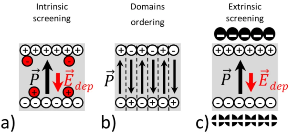
In order to stabilize the FE polarization in a finite system, in particular in configurations where the polarization is perpendicular to the surface, the depolarizing field Edep must be at least partially screened, i.e. compensated by an opposite macroscopic electric field. In real systems, Edepis screened by a macroscopic electric field that has various possible origins. Several screening mechanisms exist and are presented schematically on figure 1.5. They can be divided in two groups: intrinsic, which includes defects and domain ordering, and extrinsic.
Figure 1.5 – Different mechanisms for screening the polarization-induced charges. a) Intrinsic screening by
defects b) Domain ordering and c) Extrinsic screening mechanisms.
• Intrinsic screening:
· Defects:
Charge compensation can arise from defects and impurities inside the material itself. Vacancies or dopants inside a FE material will change the stoichiometry and lead to an excess of charge carriers that are available to screen the polarization bound charge. This screening is schematically described in figure 1.5 a). Among all the defects and impurities that can be present in oxides and have an effect on ferroelec-tricity [19,20], oxygen vacancies are the most studied. Oxygen vacancies act as donor defects to compensate the polarization bound charge [21,22]. For example, in BTO, the oxygen vacancies created by vacuum annealing generate free electrons according to OO → VO••+1
2O2+ 2e
−. The free carriers screen the positive polarization-induced charges, and may favor one FE polarization over the other, whereas the positive oxygen vacancies may screen negative polarization charges. Direct change of oxygen
1.2. Depolarizing field and screening 27
vacancy concentration can stabilize out-of-plane, inwards pointing polarization (see Ref. [23] in reduced BTO, Ref. [24] in PbTiO3). The LENSIS group reported experi-mental evidences of ferroelectric-paraelectric transition induced by doping by oxygen vacancies [25]. Since FE displacements are stabilized by long range interactions, the presence of free charge carriers (electrons or holes) in FE materials is expected to destabilize ferroelectricity. However, vacancies and impurities have been observed to induce conductivity without losing ferroelectricity [20,26,27].
· Domain ordering:
A second intrinsic screening mechanism found in FE materials is domain ordering. A "domain"İis a region of the material in which the FE polarization is uniform. The boundaries between such regions are called domain walls. Polarization can naturally form domain patterns to reduce the total energy of the system. Figure 1.5 b) shows a schematic of one type of domain ordering in a ferroelectric film. Polarization organizes itself in several domains, which can be of few micrometers to few nanometers. In this case the separations between two domains of different polarization are 180°domain walls, so the polarization in an adjacent domain is antiparallel to its neighbor. The macroscopic electric field created by each domain screens the depolarizing field in the adjacent domains. Domain ordering at the surface of BTO has been reported in several studies [28–30].
• Extrinsic screening:
Extrinsic screening can originate from polar molecules adsorbed on the surface of the FE material, free charges in electrodes, or an externally applied field.
· Adsorbates:
Extrinsic screening can be ensured by the adsorption of molecules providing surface charge compensation [24, 31, 32], as shown schematically in figure 1.5 c). Kalinin et al.used local-probe microscopy techniques, such as scanning surface potential micro-scopy (SSPM) and piezo-response force micromicro-scopy (PFM), to map the potential at FE surfaces. Evidence of complete screening of the bound charges from adsorbates was reported [33]. This study also showed that the surface charge can be fully rever-sed by a large quantity of adsorbates.
· Electrodes:
condi-tions can provide charge carriers to screen the polarization charge density. Figure 1.6 schematizes this situation.
Figure 1.6 –Schematic of an electrode/FE/electrode structure. The electrodes are in blue and the FE material
in light grey. The fixed charges, induced by the FE polarization P , are (imperfectly) screened by free charge carriers.
The free charges brought by the metallic electrodes (in blue) will accumulate at the interface with the FE material, screening at least partially the depolarizing field (red arrow). This allows maintaining polarization (black arrow) inside of the material. At the metal/FE interface, a region of space charge is created in the metal which generates a macroscopic electric field across the FE, thus screening the depolarizing field. This screening mechanism is complex and depends on the metal/FE interface which is characterized by a finite screening length, interface chemistry and strain. To integrate FE films in functioning devices, the presence of electrodes is indispensable to switch the polarization. This screening mechanism is thus of great interest.
1.2.3
Screening length
The screening length is a key parameter in the description of this last screening mechanism. Two hypothetical boundary conditions are often used for modeling or calculations:
• In the short-circuit boundary conditions, the FE charges are perfectly screened. The depolarizing field is zero.
• In the open-circuit boundary conditions, the FE charges are not screened at all. The depolarizing field is maximal.
In a real system, the screening mechanism is imperfect, with screening charges spatially distributed away from the surface of the ferroelectric, leading to finite interface dipole.
Consi-1.2. Depolarizing field and screening 29
dering identical metallic electrodes at both surfaces of the FE slab of thickness d, the total voltage drop is:
∆V = 2λef f ε0
|P | (1.7)
where λef f is the effective screening length. λef f is a measurement of the displacement of the screening charge from the FE surface. It models the distance over which the polarization charges are screened. In the case of short-circuited conditions (i.e. both metallic electrodes are at equipotential), the equation 1.6 gives for the depolarizing field:
Edep = −2 λef f
dε0
P (1.8)
The schematic of Figure 1.7 shows the relationship between the different parameters of these equations.
Figure 1.7 – Schematic of an electrode/ferroelectric/electrode structure (top). The fixed charges, induced
by the FE polarization P, are imperfectly screened by free charge from the metallic electrode over the effective screening length λef f. The resulting electrostatic potential V (bottom), or equivalently the depolarizing field Edep, acts against P .
A small screening length means good screening by the electrodes, therefore a weak depolari-zing field, and a better FE stability. This screening length can be estimated from experimental results [34] or obtained from ab-initio calculations using electrode/FE supercells [35, 36]. Re-cently, a theoretical framework emerged from effective Hamiltonian methods. Ponomareva et al. used a screening factor to model the efficiency of screening [37]. This model has been success-fully used in many FE systems [38,39] with the advantages of effective Hamiltonian framework (large clusters, temperature dependence).
1.3
SrRuO
3, a metallic oxide electrode.
In 1999, SrRuO3, designated SRO for short, appeared on the International Technology Road-map for Semiconductors in the context of stacked-capacitor dynamic random access memory. As recognized early on by Eom et al. (1992) [40], metallic SRO is a good candidate because of its perfect registry with several substrate materials and its nearly ideal growth mode. In their work, Schlom et al. [41] present the lattice constant of several perovskite or perovskite-related phases along with several substrate ones. This comparison is schematically presented in figure 1.8.
Figure 1.8 –A number line showing the pseudotetragonal or pseudocubic a-axis lattice constants in angstroms
of some perovskites and perovskite-related phases of current interest (above the number line) and of some of the perovskite and perovskite-related substrates that are available commercially (below the number line). From ref [41].
The work shows that the SrTiO3 substrate presents a good match with the lattices of both the BTO and the SRO. This results in single crystalline, atomically smooth thin films. The most prominent example has been the successful use of SRO in FE perovskite capacitor structures, as first demonstrated by Eom et al. (1993) [42] in the case of a Pb(Zr0.52Ti0.48)O3 structure. Numerous oxides have been used in combination with SRO electrodes (ferroelectrics such as BiFeO3 [43], dielectrics [44], and other materials [45]).
a) Crystalline structure
SRO is the infinite-layer material (n = ∞) in the series of ruthenates Srn+1RunO3n+1. Similarly to many ABO3 perovskite compounds (such as BTO for instance, as previously explained in section 1.1.3), SRO exhibits orthorhombic structure at room temperature,
1.3. SrRuO3, a metallic oxide electrode. 31
as depicted in Figure 1.9.
Figure 1.9 – Schematic view of the orthorhombic unit cell of SRO. From Gan et al. [46].
An orthorhombic cell is typically observed in ABO3 perovskites when the A-O bond length is less than twice the B-O length, which results in rotations of the BO6 octahe-dra. In SRO, the RuO6 octahedral rotation produces a distorted, pseudocubic perovskite structure, with lattice parameters a = 5.5670 Å, b = 5.5304 Å, and c = 7.8446 Å [47]; the pseudocubic lattice constant is a = 3.93 Å. The orthorhombic phase can be visua-lized by rotation of BO6 (RuO6) octahedra counterclockwise about the [010] and [001] directions and clockwise rotation about the [100] direction of an ABO3 cubic perovs-kite (pseudocubic with a = 3.93 Å); these directions become inequivalent upon rotation. With increasing temperature, the degree of the orthorhombic distortion decreases, and the structure transforms to higher-symmetry perovskite structures.
As described by Kennedy and Hunter in 1998 [48], around 550℃, the orthorhombic structure transforms into a tetragonal structure (with space group I4/mcm). In this te-tragonal unit cell, the RuO6 octahedra are rotated only about the [001] SRO direction. Going to higher temperatures around 680℃, tetragonal SRO transforms into a cubic structure (with a standard perovskite space group Pm3m), where the RuO6 octahedra are not rotated. These phase transformations are illustrated in Figure 1.10. The structu-ral transition temperatures are influenced by strain, and, hence, in the case of epitaxial
thin films, they depend on the substrate material.
Figure 1.10 – A sequence of phase transitions of unstrained bulk SRO from orthorhombic to tetragonal and
then cubic symmetry at 547℃and 677℃, respectively. The unit cell of the orthorhombic SRO consists of four formula units of the ideal cubic perovskite structure. The atoms of Ru occupy high-symmetry positions with respect to the orthorhombic shape of the cell. The atoms of O and Sr are displaced from their high-symmetry positions due to the octahedral tilting. The tetragonal SRO is a one-tilt system, where RuO6octahedra are rotated only about the [001] direction. The cube corresponds to the unit cell of each SRO form. Gray, black, and white balls represent Ru, O, and Sr atoms, respectively. From Choi et al. [49].
Moreover, it is important that the electrodes grow epitaxially on both the BTO and the STO substrate. As the SRO has a small mismatch with BTO and STO, it will epitaxially grow on them, with little to no interfacial defects [50]. It has already been shown that SRO grows epitaxially on these materials [51].
b) Electronic properties
SRO is often used as an electrode. There are several reasons for this. It is one of the few complex oxides that are metallic without external doping. Indeed several oxides, such as SrTiO3, need to be doped with metals such as niobium to be conducting. SRO has a good lattice match with a wide variety of functional oxides and therefore is relatively easy to incorporate in heterostructures. Thus, thin films of SRO have drawn wide interest as a conducting layer in epitaxial multilayered structures of complex oxides, in particular, as electrodes in oxide electronics.
The basic electronic structure of SRO can be obtained by developing its energy level structure from atomic orbitals, as depicted schematically in Figure 1.11.
1.3. SrRuO3, a metallic oxide electrode. 33
Figure 1.11 – Schematic low-spin one-electron energy level diagram for a perovskite ruthenate ARuO3. The degeneracies of the bands indicated in square brackets are multiplied by 2 to allow spin degeneracy. The correlation lines indicate the dominant atomic parentage of the band states. From Cox et al. [52].
As the diagram shows, the fivefold degeneracy of the Ru 4d orbitals is broken into two groups by the octahedral crystal environment, raising the energy of the 4d(eg) levels above the 4d(t2g) levels. When the three 4d(t2g) levels are filled with four electrons ac-cording to Hund’s rules, the resulting spin state is S = 1. These simple arguments allow one to anticipate the band structure. Early first-principle band structure calculations for SRO were published by Allen et al. [53] and by Singh et al. [54]. Both calculations correctly predicted that SRO is an itinerant ferromagnet. Figure 1.12 shows the spin-resolved density of states (DOS) from Allen et al. [53], which indicates a Stoner splitting of nearly 1 eV between the majority and minority bands, together with a significant DOS for both at the Fermi level. As expected from the figure 1.11, the states near the Fermi level have predominantly Ru 4d(t2g) and O 2p character.
Figure 1.13 shows the resistivity of SRO as a function of temperature. The drop in resistivity at T = 160 K reflects the ferromagnetic transition. At higher temperatures the resistivity continues to rise, into becoming a "bad" metal, i.e. badly conducting [53,55]. In the case of our study, this could be an issue as the SRO used as an electrode needs to be conducting to apply a bias on the FE BTO. We thus avoided any over-heating of
Figure 1.12 – Electronic density of states of ferromagnetic SRO. Majority spin is plotted upward, minority
spin downward. The cell contains four formula units. From Allen et al. [53].
the samples. At low temperature, conventional metallic behavior is observed.
Figure 1.13 – Resistivity vs temperature for SRO. From Allen et al. [53].
1.4
Metal / ferroelectric interface - state of the art
The integration of FE materials in electronic devices requires two electrodes for application of a bias to switch the polarization state. One issue is that the screening provided by elec-trodes is sometimes less effective than the one provided by external adsorbates on the FE or by natural rearrangement of domains. To properly maintain the ferroelectricity, the nature and characteristic of the electrodes have to be carefully chosen, in order to provide good enough screening of the depolarizing field, along with efficiently playing their role as conductor for the
1.4. Metal / ferroelectric interface - state of the art 35
electrical contact between the material and the circuit. A second issue, is the need to properly control the interface chemistry, in order to maintain the desired symmetry between the two polarization states.
Metallic electrodes under short-circuit conditions should provide a mechanism for compen-sation of the depolarization field that acts to stabilize the uniformly polarized state. However surprisingly, with pure metal electrodes, the screening is often imperfect. Indeed as the FE films get thinner, the residual field in the ferroelectric due to the surface-dipole density at the ferroelectric/electrode interface grows [35,56] resulting in a renormalization of the coercive field [3], and ultimately a possible destabilization of ferroelectricity in the thinnest films. Thus, researchers have started to focus on the possibility of other electrodes such as semi-conducting oxides to provide better screening. These materials have been found to be more efficient than pure metal electrodes.
1.4.1
Ferroelectricity in ultrathin films
Promising new properties appear when reducing dimensions of thin films, dots, wires or clusters to the nanometric scale. The physics at this scale is of great interest since quantum-related phenomena can be dominant. The potential industrial applications in the long-standing quest for nanotechnology, high-storage density or low-consuming devices are very promising. Recently, the growth of strained, nanometer-thick, oxide films has met some significant develop-ments [57, 58] ; therefore a lot of research in material science has focused on oxide multilayers. In 2008, D. Schlom wrote in a review of oxide films:
"Oxides exhibit the full spectrum of electronic, optical, and magnetic behavior: insulating, semiconducting, metallic, superconducting, ferroelectric, pyroelectric, piezoelectric, ferromagne-tic, multiferroic, and nonlinear optical effects are all possessed by structurally compatible oxides" [58].
The use of oxide heterostructures may thus allow one to taylor an extremely wide range of physical properties, especially when strain-engineering is used [41,59]. In the field of FE based electronics, downscaling has also driven research towards novel nanoscale systems [60, 61], for instance with the development of FE tunnel junctions. It was demonstrated that in the case of ultrathin, or tunneling (thickness < 5 nm) FE films, these devices can exhibit a high FE polarization magnitude [62]. This raises the question on how the polarization behaves when decreasing the thickness of the FE film, how the polarization magnitude changes and how the
energy of the thin film accommodates for the increasing depolarizing field.
Based on early experiments, it was believed that the ferroelectricity vanishes below a critical thickness of severral microns. Then, studies suggested that it disappeared below a few tens of nanometers, due to the depolarizing field produced by polarization charges on the two surfaces of the FE film [63]. A study by Garcia et al. on FE tunnel junctions has lowered this thickness limit in BTO to only one nanometers [64].
In theoretical studies, significant progress was made in the field. Using ab-initio methods, Junquera and Ghosez [35] studied the critical thickness of BTO thin films to maintain fer-roelectricity and paved the way for numerous simulations on real device-like heterostructures of ferroelectrics thin films between two electrodes [36, 65, 66], free-standing layers under an applied electrical field [67] or domain walls [68]. Using Monte-Carlo methods, complementary information was obtained by simulating systems with realistic size and subjected to adjustable boundary conditions. They predict different domain ordering in thin films subjected to increa-sing depolarizing field [69] or the evolution of the Curie temperature with thickness [70].
In experimental studies, measuring the polarization itself is made very difficult in devices of reduced size [71]. Piezoresponse Force Microscopy (see section 2.1) can be used to prove the existence of polarization in a very thin film, and thus was often used to probe and determine the critical thickness for several types of films [72–75]. In tunnel junctions however, the leakage current is too high and prevents one from accessing the value of the switching current [76]. Studies thus often rely on other properties of the FE film that are more easily measured and that are linked to the polarization (i.e. that will be modified accordingly to any change in the polarization). For instance, Lichtensteiger et al. measured the tetragonality of the film (c/a ratio) in a PbTiO3 thin film using X-ray diffraction, as this parameter is directly related to the Ti off centering, i.e. the polarization [77]. A second example is the study by Maksymovych et al. of the out-of-plane piezoresponse of BiFeO3 thin films, expressing this response as a function of the polarization [78]. In perovskite FE oxides, ferroelectricity was observed in nanometer thick films [64,77,79]. These experimental results are consistent with the first-principles calculations predicting that the critical thickness for ferroelectricity in perovskite films can be as small as a few lattice parameters [35].
In the theoretical work on the thickness dependence of ferroelectricity carried out by Jun-quera and Ghosez [35] already cited, the role of the electrode material used was also investigated. The most notable result of this work is shown in Figure 1.14, where the evolution of the energy is measured as a function of the soft-mode distortion, and in compared to calculations on
metal-1.4. Metal / ferroelectric interface - state of the art 37
oxide systems [36, 80]. First-principles results (symbols) and electrostatic model results (lines) are shown for different thicknesses of the FE thin film.
Figure 1.14 – Evolution of the energy as a function of the soft-mode distortion ξ. The magnitude of ξ is
reported as a percentage of the bulk soft-mode displacements of BTO atoms (ξ = 1 corresponds to the distortion of the bulk tetragonal ferroelectric phase). From Ref [35].
Other work, carried out for instance by Kohlstedt et al. [81] or Nagarajan et al. [51] also in-vestigated the role of the electrode. It was predicted that the chemistry of the ferroelectric-metal interfaces strongly influences the FE state through the formation of intrinsic dipole moments at the interfaces, as determined by the atomic species and interfacial metal-oxide bonds. For some interfaces, these dipole moments are switchable and may enhance the FE instability of the thin film, which is interesting for engineering the electrical properties of thin-film devices [36]. For other interfaces, however, the effect of interface bonding is detrimental and leads to the freezing of polar displacements in the interfacial region, thus resulting in a ferroelectrically inactive layer near the interface [82]. In electrode/FE/electrode heterostructures, a skewing of the valence and conduction bands in the ferroelectric at the interface with the electrode has also been reported [65]. This modification of the bands structure allow us to access, and even control the electronic properties of such heterostructures.
1.4.2
Ionic displacement (rumpling) at the electrode/ferroelectric
in-terface
It was demonstrated that in addition to the screening associated with free charges in the metal electrodes [63] there is an important contribution resulting from ionic screening if elec-trodes are metallic oxides, such as SrRuO3 [83]. This screening results in an ionic displacement which is called rumpling. It is a common behavior of oxides. In the case of BTO, rumpling is present in the bulk due to polarization induced displacements, but will be different at the surface of the film, and thus at the interface with any other film. The electrode/BTO interface of a device-like heterostructure will thus be impacted by this phenomenum.
In a crystalline bulk, the equilibrium positions of the atoms result from a balance bet-ween the forces generated by all their neighbors. At the surface, the atoms have a different environment: some neighbors are missing with respect to the bulk. Thus, the atoms relax to equilibrium positions that differ from the bulk ones. The new equilibrium positions of the surface atoms involve displacements perpendicular to the surface. The rumpling is defined by the relative displacements, normal to the surface, of the cations with respect to the anions. At the oxide surface, it usually consists of anions displaced outwards with respect to cations. Such displacements were measured in SrTiO3 oxide by both reflection high-energy electron diffraction (RHEED) [84] and low-energy electron diffraction (LEED) [85]. On BTO surfaces, first-principles calculations [60, 86, 87] predict similar results. The relative displacements in-duced by the rumpling correspond to polar displacements, related to FE polarization at the surface. The average displacement (normal to the surface) of the cations and anions of a gi-ven plane defines the surface relaxation. The observed tendency is a reduction of interplanar spacing, at least between the surface layer and the first surface underlayer [88]. The further away from the surface atomic layer, the weaker this effect, as the properties tend to approach those of the bulk. The surface of a FE BTO(001) single crystal was studied by Pancotti [89] using synchrotron radiation induced X-ray photoelectron diffraction (XPD). The rumpling and interlayer relaxation was determined by comparing XPD results on the Ba 4d, Ti 2p, and O 1s orbitals with multiple scattering simulations for the different polarization states. The results are presented in Figure 1.15. As we can see, the rumpling corresponding to the FE distortion increases as we go from the surface of the BTO towards the bulk, whyle the oxygen atoms are relaxing to their original position.
Thus, free charges from electrodes and fixed charges redistribution via rumpling in the FE or/and in the electrode may combine to screen the depolarizing field and help maintaining the
1.4. Metal / ferroelectric interface - state of the art 39
Figure 1.15 –Relaxation and rumpling for the first four atomic layers in a) P↑ and b) P↓ domains obtained
from the Ba 4d XPD. The original and relaxed atomic layer positions are indicated by dotted and solid lines, respectively. The atomic displacements are multiplied by 10 for clarity. Ba atoms are represented in blue, oxygen in red and titanium in green. From Ref [89].
polarization in the FE film. Indeed, rumpling will change the pollarization charges ditribution in the FE. In the electrodes, rumpling will act to increrase the screening phenomena, thus reducing the depolarizing field, and helping maintain the polarization.
1.4.3
Switching kinetics of ferroelectric capacitors
The traditional approach used to describe the switching kinetics of ferroelectrics is the Kolmogorov-Avrami-Ishibashi (KAI) model [90], based on the classical theory of Kolmogorov [91] and Avrami [92]. By assuming unrestricted domain growth in an infinite crystal, this model predicts the polarization change ∆P (t) to be:
∆P (t) = 1 − exp[−(t τ)
n] (1.9)
where n is the effective dimensionality and τ the characteristic time.
This theory considers the switching process as the phase transformation with a constant nucleation rate, with domain wall velocity as the rate-limiting parameter. However this theory is only valid for infinite crystals [93], and in the case of polycrystalline FE films, nucleation-limited models describe in a better way the switching kinetics [94].
We can distinguish different switching behavior for large capacitor (> 1 µm in diameter) and smaller ones. Indeed for small capacitors, a strong effect of the electrode perimeter will induce
larger contribution of the domain wall motion in the polarization reversal process [95,96]. This theory needs direct studies of the switching kinetics to gain further theoritical interpretation. However, characterizing the domain kinetics in FE films proves to be difficult, due to a lack of experimental methods for such experiments. Indeed, the small capacitor size (> 1 µm in diameter) also pairs with very low switching times (well below 100 ns [97,98]).
A study by Gruverman et al. in 2008 succesfully attempted to investigate FE capacitor switching on a microsecond time scale for the first time, establishing a direct relationship between the polarization P (t) and the domain kinetics. Using piezo force microscopy to image FE domains during switching, they showed that the scaling effect on the polarization reversal process is indeed governed by different rate-limiting mechanisms in the case of larger and smaller capacitors. For larger capacitors, the switching behavior can be approximated using the nucleation-limited model, whereas for the smaller capacitors, this models no longer applies and might correspond to a reversal governed by domain wall motion. It as been showed these small capacitors will switch faster at high fields, and slower at low fields, whereas it is the opposite for larger capacitors.
1.5
Conclusion
In this chapter, the concept of ferroelectricity was introduced, using BTO to illustrate the phenomena occurring when leading to FE polarization (such as the phase transitions in the BTO). The main issue regarding the stabilization of ferroelectricity in thin films, due to the depolarizing field, can be overcome by different mechanisms of screening. The use of metallic oxide electrodes is especially efficient, and needed in real-like devices. This introduces the core of this thesis, i.e. the study of the top electrode/FE interface in electrode/FE/electrode heterostructures with metallic oxide electrodes. At this interface ionic displacement, rumpling, is especially helpfull to screen the depolarizing field.
Chapter 2
Experimental considerations
In this chapter, we will introduce the experimental techniques used to investigate the in-terface between the FE BaTiO3 and the different electrodes used, SrRuO3 and Au/Co. To ensure that the samples are ferroelectric, several characterization techniques such as C-V and I-V measurements, P.U.N.D. and Piezo Force Microscopy were used. The functioning details of these tests will be presented in the first part of this chapter. In the second part, we will introduce photoemission spectroscopy in general, and then the specific techniques (hard X-ray photoemission spectroscopy, photoelectron emission microscopy and hard X-ray photoelectron emission microscopy) used to investigate the device interfaces.
2.1
Ferroelectricity characterization techniques
2.1.1
Direct measure of the ferroelectric polarization
The defining feature of the electrical properties of a ferroelectric material is how its po-larization P behaves in presence of an electric field E. Obtaining P as a function of E gives key information, such as remnant and saturation polarization (PR, PS) and coercive fields (EC+, EC−). However, it is not possible to directly measure the polarization vector itself. To access this value, one has to quantify the variation of polarization when applying an electric field. In Polarization-Field (P − E) loops, the current flowing through the ferroelectric material is measured while applying a voltage. This current is directly related to the change in polarization when it is switched by the electric field.
Figure 2.1 a) shows a P − E loop for an ideal ferroelectric material. From the origin of the graph, the applied bias first brings the FE material in one of the saturated polarization states (here the P↑ state, represented by the dashed line on the figure). Once the material reached the saturated state, it will not come back to the origin on the graph. Figure 2.1 b) shows a
Figure 2.1 – Theoretical polarization versus field curve for an ideal ferroelectric material. PR and PS are respectively the remnant and saturation polarization, and EC is the coercive field.
P − E loop in the case of a ferroelectric material exhibiting leakage. The FE hysteresis cycle is characterized by several values:
• The saturation polarization PS. It corresponds to the value of the polarization at the saturation of hysteresis. This also corresponds to the highest polarization possible for reversibility before breakdown.
• The remnant polarization PR. In the case of an ideal ferroelectric material with a nearly square hysteresis loop, it is almost equivalent to PS. (Fig. 2.1 a)). However, it can be different from the spontaneous polarization. This often occurs for imperfect materials, as the capacitor might experience some leakage responsible for a loss of ferroelectricity at the remnant state, and PR will be smaller than PS (Fig. 2.1 b)).
• The coercive field EC. It is the necessary field to bring the polarization to zero. An ideal hysteresis loop is symmetrical (Fig. 2.1 a)), so the positive and negative coercive fields are equal.
The coercive field, spontaneous and remanent polarization, and the shape of the loop may be affected by many factors including the thickness of the sample, presence of charged defects, mechanical stresses, preparation conditions and thermal treatment.
In 1930, Sawyer and Tower introduced a circuit allowing measuring the hysteresis cycle of the polarization as a function of the electrical field on Rochelle Salt [99]. The principle is to measure the variation of charge (or equivalently time-integrated current) induced by a voltage sweep. A standard Sawyer - Tower circuit is shown in Figure 2.2.
![Figure 1.1 – First Polarization - Electric Field loop measured by J. Valasek on Rochelle Salt in 1920 [4].](https://thumb-eu.123doks.com/thumbv2/123doknet/12739243.357746/23.892.258.631.212.487/figure-polarization-electric-field-measured-valasek-rochelle-salt.webp)


![Figure 1.13 – Resistivity vs temperature for SRO. From Allen et al. [53].](https://thumb-eu.123doks.com/thumbv2/123doknet/12739243.357746/37.892.307.586.590.816/figure-resistivity-vs-temperature-sro-allen-et-al.webp)

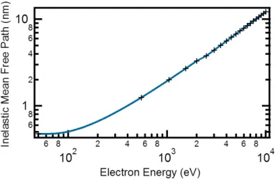
![Figure 2.14 – Universal curve of the IMFP as a function of the electron energy. (Fig. taken from [137]).](https://thumb-eu.123doks.com/thumbv2/123doknet/12739243.357746/65.892.247.653.200.451/figure-universal-curve-imfp-function-electron-energy-taken.webp)