HAL Id: hal-01159220
https://hal.archives-ouvertes.fr/hal-01159220
Submitted on 4 Jun 2015
HAL is a multi-disciplinary open access
archive for the deposit and dissemination of
sci-entific research documents, whether they are
pub-lished or not. The documents may come from
teaching and research institutions in France or
abroad, or from public or private research centers.
L’archive ouverte pluridisciplinaire HAL, est
destinée au dépôt et à la diffusion de documents
scientifiques de niveau recherche, publiés ou non,
émanant des établissements d’enseignement et de
recherche français ou étrangers, des laboratoires
publics ou privés.
Near-Field Injection At Die Level
Alexandre Boyer, B Vrignon, Manuel Cavarroc, J Shepherd
To cite this version:
Alexandre Boyer, B Vrignon, Manuel Cavarroc, J Shepherd. Near-Field Injection At Die Level.
Asia-Pacific International EMC Symposium 2015, May 2015, Taipei, Taiwan. �hal-01159220�
Near-Field Injection At Die Level
A. Boyer
#, B. Vrignon
*, M. Cavarroc
#, J. Shepherd
*# CNRS, LAAS, 7 avenue du colonel Roche, F-31400 Toulouse, France
Univ. de Toulouse, INSA, LAAS, F-31400 Toulouse, France
* Freescale Semiconductor, Inc., Toulouse 31023, France
Abstract— Near-field injection is a promising method in order to
induce local faults in integrated circuits. This paper aims at proposing a model of the coupling between the injection probe and the circuit under test. This study relies on measurements performed on a test chip by on-chip voltage sensors.
I. INTRODUCTION
Near-field injection constitutes a promising method for various applications such as electromagnetic attacks on secured circuits or investigations of integrated circuits (ICs) susceptibility to electromagnetic disturbances [1]. The injection at die level offers the advantage to locate precisely the origin of the faults induced by the coupling of the near-field disturbance. This paper attempts to clarify the nature of the coupling between the injection probe and the circuit under test by the development of a model of the coupling.
This study relies on near-field injection measurements performed on a test chip which integrates several on-chip voltage sensors for accurate characterization in high frequency of the voltage induced along circuit interconnects.
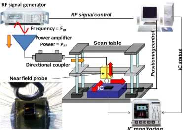
II. NEAR-FIELD INJECTION TEST BENCH
Near-field injection consists in placing a miniature near-field probe in the vicinity of a device and injecting disturbance signals in the probe to induce a local voltage fluctuation and thus trigger a failure. It relies on a near-field scan table in order to control precisely the position of the near-field probe above the device under test (DUT). The test bench is described in Fig. 1. The near-field probe is excited either by a harmonic or pulse signal. In this study, harmonic signals are used for frequency analysis purpose. One drawback of this type of signal is the major power dissipation induced in probes and cables.
Near-field injection probes are miniature and wideband antennas dedicated to the generation of either electric or magnetic fields in the vicinity of electronic components or printed circuit boards. They are usually based on small loops and opened tips. Near-field injection relies on probe with a good spatial resolution and a sufficient efficiency to induce a perceptible effect on the DUT.
RF signal control P o s it io n in g c o n tr o l
Near field probe
IC IC monitoring Scan table RF signal generator Directional coupler Power amplifier Power = PRF IC s ta tu s Frequency = FRF
Fig. 1 Near-field injection test bench
In this study, only injections with magnetic field probe are considered. Comparisons between injections with electric and magnetic field probes can be found in [1]. A handmade miniature tangential magnetic field probe based on MIL-C-17/151-00001 semi-rigid coaxial cable is developed. Its diameter is equal to 1.2 mm.
III.PRESENTATION OF THE TEST CHIP
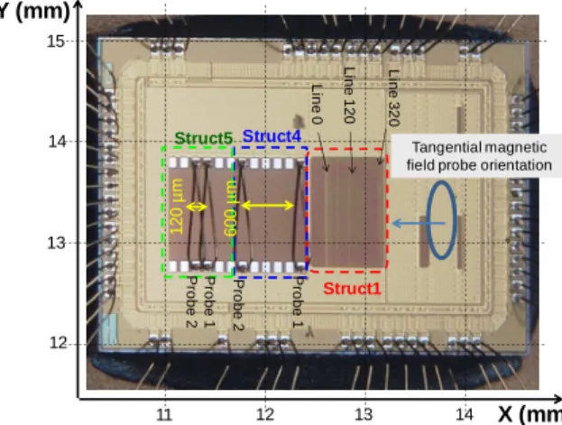
All A test vehicle has been designed with Freescale® in 0.25 µm SMARTMOS 8 technology with 4 metal layers in order to study the near-field injection on basic interconnect structures (IC metallization or bonding wires). Three structures are tested in this study, dedicated to the characterization of the coupling on IC interconnects and inter-chip bonding wires (Fig. 2). The first one called Struct1 consists in eight 1 mm lines separated by a variable distance (from 0.455 to 320 µm). The name of each line depends on the separation from the adjacent line. They are formed by a 1.75 µm wide trace routed on metal layer 3 over a reference plane Vref designed in metal layer 2. This plane is biased by an internal bandgap. The lines are terminated by 50 Ω resistors.
Y (mm) X (mm) 12 13 14 15 11 12 13 14 Tangential magnetic field probe orientation
Struct1 Struct4 Struct5 P ro b e 1 P ro b e 2 P ro b e 1 P ro b e 2 1 2 0 µ m 6 0 0 µ m L in e 0 L in e 3 2 0 L in e 1 2 0
Fig. 2 Test chip and position of the test structures
The two other structures, called Struct4 and 5, consist in two adjacent 1 mm long bonding wires, separated by either 120 and 600 µm and mounted above the reference plane Vref. In Struct4, the wires are terminated by 50 Ω resistors while they are terminated by digital buffers in Struct5.
Measuring the local voltage fluctuations in an IC induced by a near-field probe is not obvious, since I/O pads and IC package introduces a non negligible attenuation and distortion. Using high frequency probes placed directly on IC pads disturbs also the measurements. A convenient and more accurate method relies on the use of on-chip voltage sensors (OCS) [2]. It aims at measuring the waveform of voltage profiles on non accessible nodes with a precise time resolution (up to 100 ps). Its isolation from noise produced by the probe is ensured by a dedicated power supply and a deep N-well substrate isolation.
Twenty four OCS are disseminated within the test chip, at the end of each line structures. OCS reconstruct the time-domain waveform of signal induced by the near-field injection. Characteristics such as amplitude or phase of the induced signal can be extracted according to probe type, position, orientation or excitation signal.
IV.EXPERIMENTAL RESULTS
A. Results on Struct1 - Coupling on IC Interconnects
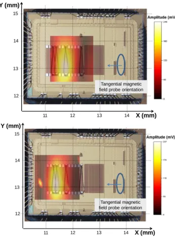
Fig. 3 presents the distribution of the amplitude of the signal coupled on line 0 when the probe is positioned at 400 µ m above the surface of the die. The probe is excited by a 400 MHz sinusoidal signal. Its power is set to PRF = 20 W.
A large voltage fluctuation that exceeds several hundred of millivolts is recorded if the probe is placed on an area of about 300x1000 µm above line 0. Similar voltage coupling is observed on other lines of Struct1, except that the position of the maximum coupling is above the considered line. The resolution of the probe is limited by its own size and the distance to the DUT. The nature of the coupling is magnetic: turning the probe orientation by 90° reduces the coupled voltage on the lines of Struct1.
Y (mm) X (mm) 12 13 14 15 11 12 13 14 Tangential magnetic field probe orientation
Fig. 3 Coupled voltage on Struct1 interconnects (line 0) according to the probe position (FRF = 400 MHz, PRF = 20 W)
Fig. 4 presents the induced voltage vs. frequency of the voltage amplitude coupled on line 120 µ m. Voltage fluctuations of several hundreds of millivolts can be generated on a 1 mm long IC interconnect, which can be just enough to start triggering failures in digital or analog ICs. The coupling increases with frequency as expected according to field-to-line theory. Although the coupling increases with frequency according to a typical +20 dB/dec asymptotic behaviour, this trend tends to +10 dB/dec above 100 MHz.
Fig. 4 Induced voltage vs. frequency on interconnect of Struct1 (Line 0)
B. Results on Struct4 - Coupling on Bonding Wires
The same experiments are repeated with Struct4 and 5 in the same conditions. Fig. 5 shows the evolution of the amplitude of the signal coupled on bonding wires of both structures. The coupling is maximal when the probe is placed just above the bonding wire. At 400 µ m above the die surface, the probe has enough resolution to distinguish the coupling between two wires separated by 120 µm.
Y (mm) X (mm) 12 13 14 15 11 12 13 14 Tangential magnetic field probe orientation
Y (mm) X (mm) 12 13 14 15 11 12 13 14 Tangential magnetic field probe orientation
Fig. 5 Coupled voltages on Struct4-probe 2 (top) and Struct5-probe 1 (bottom) according to the probe position (FRF = 400 MHz, PRF = 20 W)
Fig. 6 presents the evolution of the voltage amplitude coupled on bonding wires of both structures according to the excitation source frequency. The same amount of voltage is coupled on both structures. The asymptotic behavior of the coupling evolution is similar to the one observed on Struct1.
Fig. 6 Induced voltage vs. frequency on bonding wires of Struct4 (probe 1) and Struct5 (probe 1)
V. MODELLING OF THE COUPLING
Fig. 7 presents the general methodology dedicated to the simulation of the coupling between the injection probe and the lines under test in frequency domain.
1. H field probe electrical model Probe model RF generator IRF(f) IRF 2. Emitted magnetic field H ( ) ( )P A( )P H dl r e I P A probe r j r r r × ∇ = = ∫ − 0 0 1 4 µ π µ β 3. IC interconnect model 4. Load model Si P++substrate SiO2 VREFplane IC lines 5. Field coupling modeling 6. SPICE simulation Coupled voltage vs. frequency
∫
+ = Lline O line L L L H j H h dl Z Z Z V 0 tan 2 1 1 ωµFig. 7 Modelling flow
C. Modelling of the injection probe
An electrical model of the magnetic probe is developed to compute the excitation current according to the frequency (step 1). The magnetic field produced by the probe is directly related to the excitation current (step 2). Given the small size of the injection probe, a lumped electrical model can be constructed, where the magnetic probe is mainly inductive. Its inductance can be determined by electromagnetic simulations or analytic expressions, e.g. [3]. Parasitic capacitor and resistors due to ohmic and radiation losses can be added to improve the model at high frequency. The magnetic field produced by the probe at any point may be evaluated according to the magnetic dipole approximation but the accuracy is limited at very close distance. It is necessary to integrate the contribution of the current flow along the probe.
D. Modelling of the circuit under test
The magnetic field produced by the injection probe is mainly coupled on IC interconnect such as bonding wires or long metal lines. The coupling depends on the line configuration and length (step 3), but also on its loading (step 4). Load models are extracted from circuit netlist, which may be annotated by a post-layout simulation to include parasitic elements introduced by IC metallization and devices.
The configuration of the tested lines are quite complicated since they are formed by several conductors (e.g. parallel metal lines over Vref plane over IC substrate) with non-linear frequency dependence. A fundamental line configuration is microstrip line designed on Si-SiO2 substrate. The electromagnetic behaviour of this complex structure may be described according to [4]. The nature of the propagation is related to the frequency and Si substrate resistivity. Our test chip is designed on a highly conductive P+ substrate. Slow-wave and skin-effect propagation modes dominate in low and high frequency respectively. Equivalent frequency-dependent RLCG models can be extracted for each of these modes.
E. Field coupling to IC interconnects
As the coupling is magnetic, it may be modelled either by a mutual inductor or by an equivalent voltage generator distributed along IC interconnects (step 5). From the magnetic
field produced by the injection probe and the line configuration, it can be easily computed on a two conductor transmission line according to Taylor's model. This method can be also extended to the case of multi-transmission line [5]. Finally, the different elements of the model can be simulated with a SPICE simulator in order to compute the evolution of the coupling according to the frequency, probe nature and position (step 6).
F. Comparison with measurement
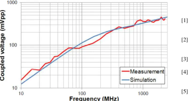
The proposed methodology is applied in order to model the coupling between the miniature injection probe and the lines of Struct1. The magnetic field is coupled on a complex equivalent line formed by the narrow traces designed in metal layer 3 and routed above the reference plane Vref. The line also includes the P+ substrate below the plane Vref. The 50 Ω load, the input impedances of the bandgap reference and the sensors are connected on the different terminals of this line. Fig. 8 presents the comparison between the simulated and measured coupled voltages on the line0 of Struct1 in frequency domain, which are in a good agreement. The 10 dB/dec asymptotic behaviour observed above 100 MHz is due to the high conductivity of the substrate.
Fig. 8 Comparison between measurement and simulation
VI.CONCLUSIONS
Near-field injection is a promising method for applications such as electromagnetic attacks on integrated circuits or investigations of their susceptibility. Modeling this method is essential to optimize the injection method, understand the origins of triggered failures and develop efficient countermeasures against electromagnetic attacks. The paper has presented a model of the coupling between a magnetic field injection probe and canonical circuit interconnects. The coupling is dependent on the probe characteristics, the line configuration, its loading and the substrate resistivity. Further studies are required to test the relevance of the model on more complex structures.
ACKNOWLEDGMENT
This work is supported by the French Agence Nationale de la Recherche under contract ANR-12-INSE-005 E-Mata-Hari.
REFERENCES
[1] A. Boyer, B. Vrignon, J. Shepherd, M. Cavarroc, " Evaluation of the Near-Field Injection Method at Integrated Circuit Level", EMC Europe 2014, Gothenborg, September 2014.
[2] S. Ben Dhia, E. Sicard, F. Caignet, “A new method for measuring signal integrity in CMOS ICs”, Microelectronic International Journal, Vol. 17, No. 1, January 2000.
[3] M. Kanda, "Standard Probes for Electromagnetic Field Measurements", IEEE Trans. on Antennas and Propag., vol. 41, no 10, October 1993. [4] H. Hasegawa, M. Furukawa, H. Yanai, "Properties of microstrip line
on Si-SiO2 system", IEEE Trans. on Microwave Theory and Techniques, vol. MTT-19, no 11, November 1971.
[5] C. R. Paul, "Analysis of Multiconductor Transmission Lines - 2nd Edition",Wiley, 2008.