Solid State Physics, Electronics
and Optics
Section 1
Section 2
Section 3,
Section
4
Materials
and
Fabrication
Quantum-Effect Devices
Optics
and
Devices
Surfaces
and
Interfaces
Section 1
Chapter 1
Chapter 2
Chapter 3
Materials and Fabrication
Compound
Semiconductor Materials and Devices
Physics of InAlAs/InGaAs Heterostructure
Field-Effect Transistors
Epitaxial Growth and Processing of
Chapter 1. Compound Semiconductor Materials and Devices
Academic and Research Staff
Professor Clifton G. Fonstad, Jr.
Visiting Scientists and Research Affiliates
Norio lisuka,' Dr. Sheila Prasad,2 Masami Tachikawa,3 Praveen T. Viadyananthan2
Graduate Students
Rajni J. Aggarwal, Joseph F. Ahadian, Henry K. Choy, Donald S. Crankshaw, Isako Hoshino, Paul S. Martin, Janet L. Pan, Steven G. Patterson, Yakov Royter, Hao Wang
Undergraduate Students
Wojciech P. Giziewicz, Karen Waithe4
Technical and Support Staff
Olga M. Arnold, Charmaine A. Cudjoe-Flanders, Angela R. Mickunas
1.1 Introduction
Heterostructure devices, such as laser diodes and high-electron mobility transistors, play an increas-ingly important role in our lives as the key, enabling components of such common items as compact disk players, cellular telephones, fiber communica-tion links, and direct broadcast television receivers. The impact of heterostructure devices would be even greater, however, if they were not limited to applications involving single devices or combina-tions of a few devices. These applications are limited due to the enormous cost of developing an integrated circuit technology comparable to that which exists for silicon. Addressing this bottleneck, researchers in Professor Clifton Fonstad's research group at the MIT Research Laboratory of Elec-tronics have recently made major advances in inte-grating complex compound semiconductor heterostructures with commercial very large-scale integration (VLSI) electronic circuits. The epitaxy-on-electronics (EoE) technology we have developed
in collaboration with Professor Leslie A. Kolodziejski, another RLE researcher, promises to make practical fabrication of complex integrated heterostructure systems such as image recognition sensors, massively parallel neural computers, hand-held retinal scanners, and similar items now more commonly associated with science fiction than reality.
The following sections describe Professor Fonstad's research program and key results obtained during the past year. Highlights include (1) significant enhancements in the EoE process (2) initiation of the OPTOCHIP Project, making EoE optoelectronic integrated circuits (OEICs) available to the user community through a research foundry offering; and (3) new work on surface-emitting laser diodes, 1550 nm photodetectors on GaAs, and quantum-well intersubband photodetectors. Work on hyper-thermal molecular beam etching, microwave device characterization, and compact integrated optics components is also reported.
1 Toshiba Corporation Ltd., Kawasaki, Japan. 2 Northeastern University, Boston, Massachusetts. 3 NTT Corporation, Atsugi, Japan.
Chapter 1. Compound Semiconductor Materials and Devices
1.2 Epitaxy-on-Electronics Integration
Technology
Sponsors
Defense Advanced Research Projects Agency/ National Center for Integrated Photonics Technology
Joint Services Electronics Program Grant DAAH04-95-1-0038 MIT Lincoln Laboratory National Science Foundation
Graduate Fellowship
U.S. Navy - Office of Naval Research
Project Staff
Joseph F. Ahadian, Yakov Royter, Steven G. Patterson, Hao Wang, Praveen T. Viadyananthan, Paul S. Martin, Rajni J. Aggarwal, Dr. Gale S. Petrich, Professor Leslie A. Kolodziejski, Professor Clifton G. Fonstad, Jr., in collaboration with James M. Mikkelsons Dr. William D. Goodhue6
Implementation of optical interconnects will require monolithic OEICs consisting of thousands of opto-electronic devices tightly integrated with VLSI-complexity electronics. LED-based neural-network OEICs have previously been demonstrated using the epitaxy-on-electronics (EoE) process developed at MIT. However, the utility of this work was limited by a number of process shortcomings; our recent work has focused on process inno-vations overcoming these shortcomings and resulting in a more robust, practical and manufacturable optoelectronic integration tech-nology.
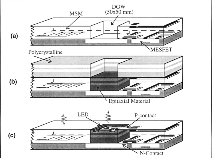
The EoE process is outlined in figure 1. Commer-cially fabricated GaAs VLSI chips are the starting point for this process. This electronic technology (the Vitesse semiconductor HGaAs3 process)
pro-vides enhancement- and depletion-mode MESFFETs and four layers of aluminum-based electrical interconnect, as well as optical field-effect transistor (OPFET) and metal-semiconductor-metal
(m-s-m) photodetectors. In the EoE process,
gas-source molecular beam epitaxy (GSMBE) is used to grow device heterostructures on regions of the GaAs substrate which are exposed by cutting through the interconnect dielectric stack. Estab-lished fabrication techniques complete the inte-gration procedure. The unrestricted placement of
the optoelectronic devices occurs as part of the routine layout of the integrated circuit; the
intercon-nect dielectric stack in the regions designated for these devices is partially etched at the GaAs foundry forming dielectric growth windows (DGWs). The etch is completed, exposing the underlying GaAs substrate, upon receipt of the ICs from the manufacturer; the design of the DGW structure and of the technique for producing a damage-free GaAs starting surface are among the latest inovations in the EoE process. Figure la shows the IC just prior to GSMBE growth. The source/drain implant is used as the bottom n-contact of the optoelectronic device. Epitaxial material is then grown in the DGWs, while polycrystalline material is deposited on the overglass, as shown in figure lb. Standard processing techniques are then used to remove the polycrystalline material, to fabricate the optoelec-tronic devices, and to interconnect the top-side electrical contacts of the devices to the electronics. Figure ic shows a completed OEIC containing LEDs.
As in standard silicon technologies, the gallium arsenide VLSI process uses aluminum-based elec-trical interconnects. We have shown that these interconnects degrade when exposed to temper-atures in excess of 475 degrees C. Conventional MBE practice uses a 580 degrees C temperature excursion to desorb the native oxide on the GaAs surface prior to growth, and even this brief high temperature exposure (which was used in previous EoE work) results in appreciable damage to the interconnect lines. Interconnect degradation is now effectively eliminated by using cracked hydrogen to remove the native oxide at as low as 350 degrees
C.
Also, owing to the electrical interconnect thermal instability, the epitaxy must be carried out below 475 degrees C. This restriction is not compatible with the growth of high quality AIGaAs suitable for emitters (although it can be used in passive appli-cations) due to aluminum's high affinity for oxygen. The performance of previous monolithic EoE light emitting diodes involving AIGaAs heterostructures was thus compromised. To circumvent this diffi-culty, current EoE efforts use the aluminum-free InGaAsP materials system, which is routinely grown a reduced temperatures. To verify the high quality of this EoE-compatible material, InGaP/GaAs/InGaAs quantum-well, separate-confinement heterostructure (QW-SCH) lasers with
5 Vitesse Semiconductor Corporation, Camarillo, California.
Figure 1. Overview of the epitaxy-on-electronicss process: (a) the pre-growth condition with a dielectric growth window; (b) after epitaxy, prior to removal of the polycrystaline deposit; and (c) a completed OEIC.
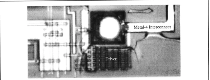
pulsed, broad-area threshold current densities, under 200 A/cm2 at room temperature, have been grown entirely at 470 degrees C. In addition, mesa-confined InGaP/GaAs light emitting diodes (LEDs) have achieved external quantum efficiencies approaching 12 pW/mA (0.85 percent). A com-pleted OEIC with an LED of this type in operation is shown in figure 2.
Process innovations in the areas of DGW prepara-tion, low temperature GaAs native oxide removal, and gas-source MBE growth of EoE compatible optoelectronic devices have removed limitations present in previous EoE demonstrations. Ring oscillator measurements made before and after EoE processing have verified stable sub-100
pico-second gate delays, consistent with sub-nanosecond, multi-gigahertz electronics operation. The present EoE technology is now being applied to a variety of applications benefiting from the inte-gration of high-performance heterostructure devices with VLSI-complexity electronics.
1.3 Monolithic Enhancement of
MESFET Electronics with Resonant
Tunneling Diodes
Sponsor
Joint Services Electronics Program Grant DAAH04-95-1-0038
Project Staff
Rajni J. Aggarwal, Professor Clifton G. in collaboration with Professor Fitzgerald, Mayank T. Bulsara
Fonstad, Jr.,
Eugene A.
Using the epitaxy-on-electronics (EoE) integration technique, we have monolithically integrated relaxed-buffer InGaAs/AIAs resonant tunneling diodes (RTDs) with GaAs MESFET VLSI circuits to build static random access memory (SRAM) cells.
Chapter 1. Compound Semiconductor Materials and Devices
Figure 2. An emitting LED and its driver FET on an EoE monolithic OEIC.
material grown on GaAs VLSI circuits is compa-rable in quality to that grown on epi-ready GaAs substrates. We also evaluated the critical RTD parameters for this application (i.e., the peak and valley voltages and current densities) over a 25
mm2 integrated circuit to quantitatively establish circuit design rules. Finally, we have demonstrated the first RTD memory cells monolithically integrated on GaAs integrated circuits.
The lack of a compact, low-power memory cell has been an important limitation of GaAs MESFET inte-grated circuit (IC) technology. Because of large junction leakage currents, dynamic memory cells of the type so widely used in silicon integrated circuits are not viable in GaAs ICs, and designers are forced to use static cells based on flip-flop circuits. These cells involve many transistors (a minimum of six, but more typically 10), consume much power, and occupy chip real estate. A compact, low-power static memory cell formed with two tunnel diodes and a single transistor has been proposed as an alternative by several groups, and other groups have proposed integrating tunnel diodes with reso-nant hot electron transistors (RHETs) and
hetero-junction bipolar transistors (HBTs) to produce
low-power III-V logic circuits. A major problem with these proposals is that they would require the development of an entire VLSI technology in order to implement them. It is in this aspect of the problem that the EoE technology offers its solution.
By building on the million dollar, multi-thousand man-year investment in technology devel-opment made by such companies as Motorola and Vitesse Semiconductor in developing their commer-cial GaAs VLSI production facilities, the EoE process leap-frogs the basic issue of developing a VLSI technology, and focuses on the issues involved in complementing that technology with monolithic heterostructure devices, in the present case, with resonant tunneling diodes.
The uniformity of device performance across an integrated circuit chip of EoE RTDs, and the simi-larity of that data to that of RTDs formed on bulk material, has important implications for optoelec-tronic device integration as well. The spreads in peak and valley current and voltage levels in each case is comparable; this is very good. On the other hand, their is a difference in the current levels, which are consistently a factor of two lower on the integrated circuit. A possible explanation is that defects originating from the ion implanted DGWs on the IC deplete portions of the RTD heterostructure, reducing the active area by two, but not otherwise effecting device performance.
The next issue to address in this program will be the question of the minimum size a growth well can have, and thereby what the ultimate packing density of RTD memory cells can be. These issues are also being addressed with respect to optoelectronic
1.4 Hyperthermal Molecular Beam Dry
Etching of III-V Compound
Semiconductors
Sponsors
AT&T Bell Laboratories Fellowship
Defense Advanced Research Projects Agency/ National Center for Integrated Photonics Technology
Joint Services Electronics Program Grant DAAH04-95-1-0038
Project Staff
Isako Hoshino, Professor Clifton G. Fonstad, Jr. With our increased interest in compound semicon-ductor epitaxial layer growth on fully processed inte-grated circuits, it has become more crucial to minimize or eliminate the surface damage caused by conventional dry etching techniques using plasma and ion sources. As a solution to the problem of plasma- and ion-induced damage, we are pursuing a project to investigate the use of hyperthermal molecular beam techniques to etch and clean Ill-V substrates and heterostructures. Depending on the gas combination employed, it is anticipated that low energy (0.1 to 5 eV) can be used to both directionally and isotropically etch Ill-V
materials.
A differentially pumped ultra-high vacuum (UHV) hyperthermal (or "kinetic") beam etch (KBE) system has been designed and constructed. The initial characterization tests of this system are currently underway, with particular attention being given to etch rate, etch profile, and surface damage assess-ment. Beams containing methane and hydrogen, chlorine, and chlorine and hydrogen have been used to date to etch indium phosphide and gallium arsenide substrates. Figure 3 shows a typical result of etching indium phosphide with xmx. As seen in this figure, preliminary indication are that what is seen is a combination of the directionality commonly seen in dry etching and the crystallo-graphically defined topology characteristic of wet-chemical etching. Work is currently in progress to more fully characterize the etching process to learn how one etch characteristic can be favored over the other, depending on the objective of a given process.
Ultimately the KBE system will be connected to the existing molecular beam epitaxy (MBE) system through a UHV transfer tube, creating an integrated UHV cluster tool for Ill-V heterostructure pro-cessing.
Figure 3. An InP substrate etched by a hyperthermal chlorine beam at a substrate temperature of 250 degrees
C. The oxide mask has been removed; the trench is
approximately 10 pm wide at the top.
1.5
InGaAsP/GaAs
Light Emitting
Diodes Monolithically Integrated on
GaAs VLSI Electronics
Sponsors
Defense Advanced Research Projects Agency/ National Center for Integrated Photonics Technology
National Science Foundation Graduate Fellowship
U.S. Navy - Office of Naval Research Project Staff
Joseph F. Ahadian, Steven G. Patterson, Praveen T. Viadyananthan, Yakov Royter, Dr. Gale S. Petrich, Professor Leslie A. Kolodziejski, Professor Clifton G. Fonstad, Jr.
A natural application of the epitaxy-on-electronics
(EoE) integration technique is to surface-normal light emitters. The least complicated emitter is the light emitting diode (LED); thus LEDs were selected as the initial demonstration vehicle so that our primary attention could be focused on the process steps unique to the integration. Extension of the EoE integration process to surface-emitting lasers
(SEL) will be straightforward after we complete
independent development of InGaAsP/GaAs SEL processes.
Mesa-confined GaAs/InGaP double-heterostructure LEDs were developed and used in the first
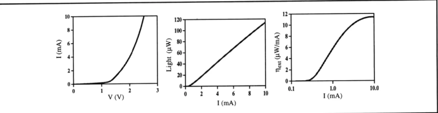
demon-Chapter 1. Compound Semiconductor Materials and Devices to 120 12 8- 100. 10 -4. 40" 20 0 gl0 0 1 2 3 0.1 1.0 10.0 V (V) 2 4 6 8 10 I (mA) I (mA)
Figure 4. Performance curves for InGaP/GaAs LEDs on bulk material; Left: terminal current verses voltage; center: light output verses input current; right: external efficiency in pW/mA verses input current.
strations of our improved EoE process for dielectric growth well and optically shielding the rest monolithic emitter-based OEICs. Using the of the circuit from the emission of the LED in the
InGaAsP materials system, high optical quality well. Full characterization of the integrated LEDs material is grown at a substrate temperature of 470 and the effectiveness of the optical shield is degrees C, which is compatible with EoE temper- planned for 1997.
ature restrictions. Conventional gas-source
molec-ular beam epitaxy (GSMBE) was used for the LEDs are not only a good device for an initial dem-growth, after first removing in situ any native oxide onstration, they are also of interest in their own on the crystal surface using atomic hydrogen, again right, and they are preferred to laser diodes in at 470 degrees C. Measurements of LEDs fabri- certain applications. Their zero turn-on current, cated on bulk wafers are shown in figure 4. Optical high linearity, and broad emission beam (i.e., lack output power levels of use in practical applications of directionality) are all attractive for some applica-are achieved at voltage and current levels compat- tions. Their main drawback is the low efficiency (on ible with the VLSI GaAs electronics. External effi- the order of 1 percent) of simple devices like those
ciencies approaching 12 pW/mA (0.85 percent) are discussed here. Considerably higher efficiency achieved, as is expected for LEDs of this geometry. LEDs can be realized if resonant cavities and photon recycling are incorporated into the device
A completed, integrated LED is shown in figure 5. design, but adding these features makes the
As illustrated in the cross-sectional drawing at the process significantly more complex and compro-right, contact is made to the back of the devices mises some of the other features of LEDs. We do using the source/drain n+ ion implant, and to the top not currently have plans to pursue these more p-contact of the diode through an aluminum metal advanced LED structures, preferring to concentrate lead patterned between the device and a contact our efforts on surface-emitting laser diodes, but our pad on the circuit chip. Not shown in the cross- work on the integration of basic LED structures can section sketch is an optical shield formed by pat- serve as an excellent foundation for work on terning rings of interconnect metal surrounding the advanced LEDs, should that be of interest.
4 nm GaAs Etch Stop
A4 nm GaAs Etch Stop Cross-section Optical Shield
TM02 9m SiO2 i (not shown in diagram)
S6.5 lm Dielectric
Stack
Figure 5. Integrated InGaP/GaAs mesa-confined light emitting diodes: (a) an artist's cross-sectional sketch, and (b)
1.6 The OPTOCHIP Project and other
Multi-group OEIC Chips
Sponsors
Defense Advanced Research Projects Agency/ National Center for Integrated Photonics Technology
National Science Foundation Graduate Fellowship
U.S. Navy - Office of Naval Research
Project Staff
Joseph F. Ahadian, Steven G. Patterson, Praveen T. Viadyananthan, Yakov Royter, Masami Tachikawa, Dr. Gale S. Petrich, Professor Leslie A. Kolodziejski, Professor Clifton G. Fonstad, Jr., in collaboration with James M. Mikkelson7
The OPTOCHIP Project is a research foundry offering intended to provide prototype OEICs to sel-ected university groups doing research on optical interconnect systems. The first generation OPTOCHIPs will use InGaP/GaAS light emitting diodes (LEDs) monolithically integrated using the epitaxy-on-electronics (EoE) technology on commerically fabricated GaAs integrated circuit chips containing optical field effect transistor (OPFET) and metal-semiconductor-metal (m-s-m) photodetectors, and enhancement- and depletion-mode metal-semiconductor field effect transistors (MESFETs). A solicitation for participation was
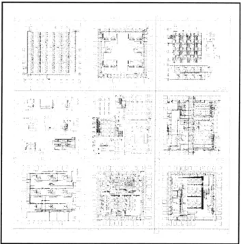
made in late 1995 and in early 1996 nine groups from eight universities were selected to participate; the universities represented are California Institute of Technology, Colorado State University, George Mason University, McGill University, Texas Christian University, University of Southern Cali-fornia, and Univeristy of Washington. These groups began work in February 1996 on the designs for 2 mm by 2 mm OEIC chips which were combined into a larger die and submitted to the MOSIS service in May 1996. A layout plot of this submission is
shown in figure 6. After electronics fabrication by Vitesse Semiconductor Corporation, the EoE inte-gration process was initiated. Fabrication of the integrated LEDs will be completed in early 1997; the completed OPTOCHIP die will be sawn in to individual 2 mm by 2 mm chips and returned to the
designers for deployment in their nect architectures. ... ... '.: ..;L .. " ''. "J -, . . ' . . ..: : -- .^ ,. .. ! : ;. ;. ._;:<-.. . .. -.g i. i ... : ' optical
intercon-':;
~:
'7-i !:
: ' :4 4- .:' -,' .... .. ...• . i!i .i . :i: :!(" L: :- <--1. ; . . j... ,. : i - i...Figure 6. The mask layout plot of OPTOCHIP-1, the multi-project OEIC chip of the initial OPTCHIP Project offering. Each of the nine cells measures 2 mm by 2
mm.
When completed, the overall 7 mm by 7 mm square
OPTOCHIP die will contain over xxx LEDs inte-grated with numerous different circuits and subsys-tems containing thousands of transistors. As such it represents on of the most complex LED-based monolithic OEICs ever fabricated, and it is unique in that it incorporates designs from a diverse selection of groups and in that minimal constraints were placed on the circuit designs. Our intention is that there will be future OPTOCHIP offerings, the next solicitaion coming sometime in 1997, and that the processing of subsequent OPTOCHIPs will be done on a semi-professional basis using the facilities of the Technology Research Laboratory (TRL) of the Microsystems Technology Laboratory (MTL) at MIT. We are anxious to make surface-emitting lasers (SELs) available to OPTOCHIP users in the near future; self-electro-optic effect devices (SEEDs) are another option, but our primary focus is on emitter-based OEICs containing LEDs or SELs.
7 Vitesse Semiconductor Corporation, Camarillo, California.
::
i:l
:& :I ---i i....:;.-~..::.iii;l
Chapter 1. Compound Semiconductor Materials and Devices
1.7 Monolithic Integration of
Vertical-Cavity Surface-Emitting Laser
Diodes on GaAs VLSI Electronics
Sponsors
Defense Advanced Research Projects Agency/ National Center for Integrated Photonics Technology
National Science Foundation Graduate Fellowship
U.S. Navy - Office of Naval Research
Project Staff
Henry K. Choy, Hao Wang, Joseph F. Ahadian, Steven G. Patterson, Praveen T. Viadyananthan, Yakov Royter, Dr. Gale S. Petrich, Professor Leslie A. Kolodziejski, Rachna J. Ram, Professor Clifton G. Fonstad, Jr.
Having been successful in monolithically integrating light emitting diodes with VLSI electronics by the epitaxy-on-electronics (EoE) technique, we are now turning our attention to integrating surface emitting laser diodes (SELs). We are pursuing both in-plane and vertical-cavity SELs since each configuration has its particular advantages in specific applica-tions. The in-plane SEL (IPSEL) effort is described in a separate section; the vertical-cavity SEL
(VCSEL) work is described below.
VCSELs consist of a small number of active quantum wells bounded above and below by highly reflecting mirrors; these mirrors are typically distrib-uted Bragg reflectors (DBRs), one with a reflectivity of 99 percent, or more, and the other (on the emit-ting side) with a reflectivity around 96 percent. Because the light resonates normal to the quantum wells, the Q of the cavity must be very high, the parasitic losses must be kept to a minimum, and the radiative efficiency in the active region must be very high. The VCSEL is thus a challenging device to produce, but the advantages it offers for many applications, i.e., batch processing, fabrication, and testing, low threshold current, and an optimal geom-etry for integration, make it an important device to add to the EoE menu. The challenges faced in integrating VCSELs by the EoE process include growing high quality DBRs at reduced temper-atures, reducing the device series resistance
suffi-ciently to obtain operating voltages under 3 V
(ideally under 2 V), and designing heterostructures with an overall height under 6.5 microns, consistent
with keeping the upper surface flush with the top surface of the dielectric stack on the GaAs IC chips. VCSELs are the subject of research at many labo-ratories but we have little experience with them on the MIT campus. Consequently we have begun a multifaceted effort to quickly come to speed with respsect to the current state of the art vis-a-vis VCSELs, and to ramp quickly up the learning curve.
In association with Professor Rajeev J. Ram, a new member of RLE, we are fabricating VCSELs using material grown elsewhere (and known to produce good devices) and a standard process sequence to develop a viable VCSEL process on campus. Simultaneously, we are growing similar GaAIAs/InGaAs VCSEL heterostructures on bulk substrates under normal growth conditions to prove out basic material quality and growth capabilities. We will then proceed, first, to refine our process to incorporate more sophisticated device features, and, second, to grow and process VCSEL heter-ostructures incorporating InGaP in the active regions and grown at temperatures compatible with EoE integration (i.e., under 470 degrees C). We propose to continue to use AIGaAs in the DBR structures, recognizing that the fact that it is grown at a reduced temperature may have less impact on the mirror performance than it has on the active regions. That this will certainly be true if we oxidize the AlAs layers in the DBRs to produce aluminum oxide layers, as is becoming common practice.
1.8 Monolithic Integration of In-Plane,
Surface-Emitting Laser Diodes on GaAs
VLSI Electronics
Sponsors
MIT Lincoln Laboratory U.S. Army - Ft. Meade
Project Staff
Yakov Royter, Steven G. Patterson, Joseph F. Ahadian, Praveen T. Viadyananthan, Dr. Gale S.
Petrich, Professor Leslie A. Kolodziejski, Professor Clifton G. Fonstad, Jr., in collaboration with Dr. William D. Goodhue8
Vertical-cavity surface-emitting lasers (VCSELs) are favored by many groups for integration, but they are not the only surface-emitting laser option, and in some cases the alternative, the in-plane
emitting laser (IPSEL), has distinct advantages. A case in point is the situation where one wishes to modulate the lasers using an auxilary electrode. When many lasers are integrated on a single chip, it may be advantageous for purposes of thermal budgeting and for minimizing thermal cross-talk between devices, to have all the devices contin-uously biased to the same current level (and
there-by disipating a constant amount of power). An intercavity electrode can be used to turn the emission on and off, without changing the total current through the device appreciably. The
effi-ciency of the system suffers, but the overall perfor-mance can be vastly improved.
We are collaborating with Dr. William D. Goodhue of MIT Lincoln Laboratory and the University of Massachusetts in Lowell to adapt a process he developed at Lincoln using chemically-assisted ion-beam etching (CAIBE) to produce vertical end mirrors and parabolic deflectors to obtain vertical emision from GaAIAs in-plane cavity quantum-well laser diodes. We have demonstrated sub-200 A/c
m2 threshold InGaP/GaAs in-plane quantum-well lasers grown at 470 degrees C, and are now working to apply Dr. Goodhue's geometry to these devices. The key is developing CAIBE for the
InGaP/GaAs system, and the challenge here is
developing an etch chemistry that simultaneously, and non-preferencially, etches both materials. This is made difficult by the presence of indium in one system and not the other and, to a lesser extent, by one being an arsenide and the other a phoshide. The chlorine-based etching done earlier is not suit-able because the InGaP can only be etched at ele-vated temperatures, and at those temperatures the GaAs is rapidly etched even without ion-beam assistance, and the etching is no longer directional. As a consequence, the CAIBE system at Lincoln Laboratory was modified to permit introduction of bromine as the etchant. Recent results obtained using bromine show much less selectivity, and com-plete characterization studies are underway. Bromine CAIBE will also soon be used to etch ver-tical end facets on in-plane lasers, prior to its use in
a full IPSEL process.
1.9 Metal-Semiconductor-Metal
Photodetectors from a GaAs VLSI
Process
Sponsors
Defense Advanced Research Projects Agency/ National Center for Integrated Photonics Technology,
National Science Foundation Graduate Fellowship NTT Corporation
Project Staff
Joseph F. Ahadian, Steven G. Patterson, Masami Tachikawa, and Professor Clifton G. Fonstad, Jr., in collaboration with James M. Mikkelson9
The HGaAs3 process from Vitesse Semiconductor,
which is available to university users through the MOSIS service, is the process used in current epitaxy-on-electronics (EoE) research at MIT. This process can be used to produce two photodetector structures: metal-semiconductor-metal (MSM) detectors, and optically-sensitive field effect tran-sistor (OPFET) detectors. An MSM detector con-sists simply of an interdigitated finger pattern of gate metal; electrically the device is two back-to-back Schottky barrier diodes with an optically active region between them. An OPFET is a metal-semiconductor field-effect transistor (MESFET) with a small width gate and large source-to-drain spacing. We have previously reported work charac-terizing the spectral response, detectivity, and speed of these two devices. The OPFET is a rela-tively slow but sensitive device, and the MSM is much faster but relatively insensitive; both have similar spectral response curves.
Of the two devices available in the HGaAs3 process, the MSM is the one of most interest because of its significantly higher speed. However, the performance of HGaAs3 MSMs is severely
com-promised because the optically active region in the standard process is ion implanted when the source and drain regions are self-aligned with the gate. We have worked with Vitesse to make minor changes in their basic process which can avoid this compromise and produce higher performance MSMs. Recently, we have tested a process modifi-cation developed by James M. Mikkelson at Vitesse. Round, 100 pm-diameter MSMs show an impulse response (10 fs pulse-width excitation) with
Chapter 1. Compound Semiconductor Materials and Devices a full-width at half-maximum of 205 ps; step
responses show rise and fall times between 0.2 and 0.3 ns; and the 3dB bandwidth is 1.2 GHz. The modified MSM process is expected to be made available to MOSIS users interested in OEIC appli-cations in some future MOSIS GaAs offerings.
1.10 Monolithic Integration of 1550 nm
Photodetectors on GaAs
Transimpedance Amplifier Chips
Sponsor
MIT Lincoln Laboratory
Project Staff
Hao Wang, Professor Clifton G. Fonstad, Jr., in
col-laboration with Dr. Jeffrey C. Livas,10 Dr. Katherine L. Hall1o
High-data rate optical communications systems require the increasingly complex integration of high-performance electronic circuits with similarly sophis-ticated optoelectronic devices. In the short run, these needs can be met by hybrid assemblies. However, the cost-performance compromises, reli-ability concerns associated with hybrid integration, and the increasing need for specialized subcircuits not commercially available make development of a monolithic integrated circuit technology extremely desirable. A monolithic optoelectronic integration technique, the epitaxy-on-electronics (EoE) process, developed at MIT for 850 nm optoelectronic inte-grated circuits (OEICs), is being extended to serve optical communication system needs at longer wavelengths, i.e., 1300 nm and 1550 nm.
The EoE process involves the epitaxial growth of compound semiconductor device heterostructures on custom-designed, commercially-processed GaAs integrated circuit chips obtained through the MOSIS service. After epitaxy, the heterostructures are pro-cessed into optoelectronic devices monolithically integrated with the pre-existing electronics, yielding
compact, reliable monolithic optoelectronic inte-grated circuits (OEICs) capable of multi-GHz opera-tion. This technology is being used to integrate 860 nm light-emitting diodes (LEDs), surface-emitting laser diodes (SELs), SEED devices, and integrated optics structures with GaAs depletion/enhancement mode electronics. The present research objectives are (1) to study the EoE growth of relaxed
InGaAIAs heterostructures for 1550 nm
photode-tectors; and (2) to fabricate and EoE integrate these devices on preprocessed GaAs integrated circuit chips. The immediate goal is to integrate monolithically matched pairs of photodetectors with transimpedance amplifiers (TIAs) to produce 10 GHz dual-balanced receiver circuits. The develop-ment of this technology will make it possible to inte-grate immediately additional signal processing electronics with the TIAs and to produce monolithic dual-balanced receiver linear arrays.
There are three main components to the present reasearch objective: (1) the growth of InP-matched
1.55 pm heterostructutes on GaAs substitute, (2) the demonstration of high speed detectors within this context, and (3) the monolithic integration of detectora and associated electronics. Using a
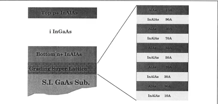
novel grading short-period superlattice (GSSL) buf-fering technology illustrated in figure 7, the first working 1.55 pm pin photodiodes have been demonstrated on GaAs substrate, as shown in figure 8. We are presently studying the effect of various buffer structures between the GaAs sub-strate and InP-matched heterostructures on the device performance (reverse leakage current and photosensitivity). We are also qualifying the newest Vitesse Semiconductor process, HGaAs sub 4, for EoE integration, because this is the process used on the highest performance TIAs from Vitesse.
Future work will expand the effort to include EoE integration of 1550 nm light emitters as well as detectors. This will require significant work on producing high-quality relaxed buffer layers on gallium arsenide with lattice constants matching that of indium phosphide under conditions compatible with the EoE process.
Figure 7. The grading short-period superlattice (GSSL) used in the buffer layer between the 1.55 pm detector layers which lattice-match indium phosphide and the gallium arsenide substrates.
35x10' 30x10 920x10" 1 5x10 10x10' o50x 10 10 15 20 25 30 Reverse Bas (V)
Figure 8. The I-V characteristics of an
Ino053Ga047As/lIn.52Al048As pin photodetector under different
illumination levels. The structure is grown on a graded
short-period superlattice (GSSL) buffer on top of the GaAs substrate.
1.11 Microwave Characterization of
Optoelectronic Devices
Sponsors
Defense Advanced Research Projects Agency/ National Center for Integrated Photonics Technology
National Science Foundation
Project Staff
Praveen T. Viadyananthan, Dr. Sheila Prasad, Pro-fessor Clifton G. Fonstad, Jr.
We have worked during the past year to expand
our microwave device characterization capabilities to encompass optoelectronic, as well as electronic, devices. By incorporating a New Focus high-speed photodetector with the HP 8510B network analyzer and Cascade probe station for on-wafer probing, a experimental set-up capable of measurements to over 20 GHz has been assembled. Our immediate objective is to thoroughly characterize the high-speed performance of the light emitting diodes (LEDs) and driver circuitry on the OPTOCHIP Project chips. The aim of the preliminary measure-ments is to model the high-frequency behavior of the LEDs and to analyze the frequency limits of the modulation characteristics of these devices. A comparison of the behavior of discrete and inte-grated devices will help in understanding the issues involved in the integration of high-speed devices unique to the epitaxy-on-electronics integration
Chapter 1. Compound Semiconductor Materials and Devices technology. An accurate estimation of device per-formance coupled with physical modeling will aid in the efficient application of LEDs as emitters in
OEICs and will also form the basis for our future
work on monolithically integrated high-speed surface-emitting laser diodes.
1.12 Reduced-Temperature Growth of
Distributed Bragg Relectors and
Monolithic Integration of
Self-Electrooptic-Effect
Devices on
GaAs on GaAs VLSI Electronics
Sponsors
Defense Advance Research Projects Agency/ National Center for Integrated Photonics Technology
National Science Foundation Graduate Fellowship
Project Staff
Hao Wang, Krishna V. Shenoy, Professor Clifton G. Fonstad, Jr., Professor Cardinal Warde, in collabor-ation with Jiafu Luo," Dr. Demetri Psaltis11
Benefiting from the novel epitaxy-on-electronicss (EoE) optoelectronic integration technique, the pursuit of integrating self-electrooptic-effect devices (SEEDs) with both enhancement- and depletion-mode MESFET VLSI circuits to produce high-density, dual-rail digital optical logic circuits has become feasible. A novel EoE-SEED process has been proposed, and the basic elements of the inte-gration demonstrated.
Dedicated SEED MESFET VLSI circuits have been designed and fabricated as part of an MIT EoE development chip, which includes featured optical
logic gates such as SEED receivers, transmitters,
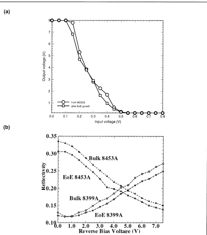
NOR gates, and more complicated logic combina-tions. In addition, a 10 X 10 SEED optical bump circuit array has been designed by our collaborators at the California Institute of Technology. After several SEED growth and fabrication efforts, the first working low-temperature regrowth SEED has been demonstrated on a chip. A respectible con-trast ratio of 2.2:1 was obtained for monolithic modulator with a 7.5 V bias, while an even better contrast ratio of 3.27:1 was obtained for a similar modulator grown simultaneously on a bulk GaAs substrate and biased to 10V (the monolithic mod-ulators are limited to 7.5 V by the breakdown voltage of the on-chip electronics). After the inte-gration, both electronics and SEED devices are working monolithically on the same chip; data com-paring the performance modulators and the drive circuitry before and after epitaxy are presented in figures 9a and b respectively.
Important issues to be addressed are whether the reduced temperature MBE growth can produce high-quality optical devices and how the optical quality at low-growth temperatures can be opti-mized. We are currently investigating lowered-temperature growth of distributed Bragg reflectors (DBRs) and multiple quantum well (MQW) heter-ostructures, which are constituent elements of VCSELs and SEEDs; we are also growing complete VCSELs and SEEDs (the VCSEL research is described in another section). The growth temper-ature constraint does not allow fully optimized quantum well formation and ideal interfacial quality in superlattices during conventional MBE. There-fore, we are exploiting alternative methods of low-temperature epitaxy, such as atomic-layer epitaxy (ALE) via MBE, pulsed-arsenic MBE, and stoichiometeric (unity group III to group V flux retio) MBE. By reducing the arsenic overpressure while staying above a unity V/Ill flux ratio, we have demonstrated AIGaAs DBRs with growth-temperature independent reflectivity down to growth temperatures as low as 400 degrees C.
(a)
7 6 5 C( > 4 0 3 2 1 from MOSIS" I- after EoE growth
0.0 0.1 0.2 0.3 0.4 0.5 0.6 0.7 0.8 Input voltage (V)
(b)
0.35
0.30 -
-.
"- "*,Bulk 8453A
0.25
'
OEoE 8453A
'
,
: 0.20
"
Bulk 8399A ,.V"
'"..
0.15
:',O,,
EoE 8399A
0 .1 0
1.0
2.0
3.0
4.0
5.0
6.0
7.0
Reverse Bias Voltage (V)
Figure 9. Performance curves for monolithically integrated SEEDs and their driver circuitry: (a) the driver output voltage as a function of the input voltage level comparing chips as received from MOSIS and prior to growth, with chips after
epitaxy, and (b) the reflectivity as a function of reverse bias at 839.9 nm and 845.3 nm for modulators grown on bulk substrates and integrated on chips using the EoE process.
Chapter 1. Compound Semiconductor Materials and Devices
1.13
Compact Integrated Optics
Structures for Monolithic
Integration
Sponsor
Defense Advanced Research Projects Agency/ National Center for Integrated Photonics Technology
Project Staff
Yakov Royter, Professor Clifton G. Fonstad, Jr., in
collaboration with Dr. William D. Goodhue12
The recent fiber-optic telecommunications boom has stimulated much work on the integration of semiconductor optical devices, such as modulators, detectors, and lasers, with driver electronics. However, the necessity to optimize both the optical and electronic devices simultaneously has made progress slow. Our group has developed a novel process to integrate mature optical components on VLSI electronic integrated circuits by selectively growing by MBE our optical devices on open areas on commercially-processed GaAs IC chips. This
epitaxy-on-electronics (EOE) technique has already
been successfully achieved for integrating LED arrays with driver circuits (see other sections des-cribing this work). Our goal in the present work is to use EoE to demonstrate a working integrated optics circuit fabricated on and integrated with a GaAs IC chip. The basic optical components of this system are passive waveguides, phase modulators, and detectors. The electronics will consist of driving and amplifying circuitry for the modulators and detectors, as well as signal processing and control digital circuits. Since the area of the GaAs VLSI chip is expensive, the conventional gradual bends necessary to change the propagation direc-tion of light guided in rectangular dielectric wavequides will be replaced by abrupt 90 degree bends with deep etched total internal reflection (TIR) mirrors.
Our first attempts at EoE integration of integrated optics components have used reduced-temperature
AIGaAs/GaAs heterostructures, grown at 500
degrees C in order not to cause drastic deteri-oration of the IC performance. However, the quality of the AIGaAs grown at such low temperatures is poor; we have measured waveguide losses greater than 20 dB/cm. Therefore, lattice-matched
InGaP/GaAs heterostructures will be used, since
InGaP grown at even 470 degrees C is of much higher quality than AIGaAs. Etching techniques for InGaP are currently being investigated in collabor-ation with Dr. William D. Goodhue at MIT Lincoln Laboratory. In particular, dry etching methods for creating deep openings with smooth vertical walls in InGaP/GaAs heterostructures are being developed. Such smooth vertical walls are necessary for the low-loss TIR mirror waveguide bends. The chal-lenge is to identify an etch chemistry that will simul-taneously etch a compound with a high indium fraction, such as InGaP, and one with little or no indium, such as GaAs or InGaAs. In this regard, recent work using bromine-based chemistries, rather than the more conventional chlorine-based systems, appears to be extremely promising.
In addition to optical device design, circuit design is also being carried out. Several versions of modulator driver circuits have been designed, fabri-cated at the Vitesse MOSIS foundry, and tested. These circuits are able to drive the modulators with a 10 V swing output with DCFL inputs of 0 to 0.6 V, with speeds of up to 5 MHz, driving external circuit board lines. Since the HSPICE simulation suggests 200 MHz performance, we expect a drastic perfor-mance improvement for these circuits driving on-chip interconnections. (The simulations were done using Vitesse HSPICE device parameters.) Complementing the modulator driver design, such fundamental issues for high-voltage MESFET circuit design as backgating and gate breakdown are investigated. Structures with depleted isolation bar-riers have been shown to eliminate backgating. Finally, a library of digital circuit cells is being com-piled for the control logic needed in the demon-stration project.
1.14 Integrated Normal Incidence
Single- and Dual-Band Quantum-Well
Intersubband Photodetectors
Sponsors
Lockheed-Martin Corporation National Science Foundation
Graduate Fellowship
U.S. Navy - Office of Naval Research
Project Staff
Janet L. Pan, Donald S. Crankshaw, Paul S. Martin, Professor Clifton G. Fonstad, Jr., in collaboration with Dr. P. Kannam13
Monolithic integration of normal incidence (trans-verse electric or TE mode) active quantum-well-infrared photodetector (QWIP) focal plane arrays (FPAs) on GaAs circuits is expected to increase the yield and processing simpicity of infarared photode-tector FPAs. FPAs are currently limited by the non-uniformity of the performance over an entire FPA and not by the detectivity of each pixel in the array.
Monolithic integration on GaAs will mean that there will be no thermal mismatch between different sub-strate materials as in a hybridized technology of GaAs QWIPs bump bonded to Si circuits; pro-cessing is also simplified because there is no need for intricate and expensive indium bump bonding. Normal incidence active QWIPs do not require
gratings to couple to the normally incident
readiation. Use of GaAs as the substrate material offers the advantages of a mature processing tech-nology: (1) the existence of large, low cost, highly uniform low-defect density substrates, as compared with mercury cadmium telluride detectors, which is required for large pixel high resolution FPAs, and (2) the intrinsic radiation hardness of GaAs, as compared with Si. The elimination of In-bump bonding and grating fabrication, as well as the use of a GaAs substitute, allow for high-yield, low-cost
QWIP FPAs. Monolithic integration can be
achieved by growing QWIPs directly on an OEIC using the epitaxy-on-electronics (EoE) technique described in other sections, or by selective area wafer bonding of a QWIP array to an OEIC, a new approach we are investigating.
We have developed a processing sequence to produce a stacked pair of QWIPs, each responding
to a different wavelength band, thereby creating a dual-wavelength, co-located QWIP array. As part of our effort to increase the signal-to-noise ratio of normal incidence QWIPs which exhibit TE-active absorption in the absence of an optical grating, we are studying ways of increasing the TE-active inter-subband absorption. While it is easy to design n-QWIPS, which rely on the intersubband absorp-tion of conducabsorp-tion band electrons, such n-QWIPs exhibit small TE-active absorption coefficents as a result of the small size of the higher order terms in the electron wavefunctions (resulting from the spin orbit and the transverse wavectors) which con-tribute to the TE-active absorption. As an alterna-tive, we are studying the intersubband absorption resulting from heavy-to-light hole transitions, which have much larger absorption strengths because of the contribution of the dominant terms in the light and heavy hole wave functions.
1.15 Figures of Merit for Quantum-Well
Intersubband Photodetector Focal-Plane
Arrays in Different Operating Regimes
Sponsor
Lockheed-Martin Corporation
Project Staff
Janet L. Pan, Professor Clifton G. Fonstad, Jr., in collaboration with Dr. R.J. Martin14
The narrow responsivity spectra of quantum-well-infrared photodectors (QWIPs), as well as our ability to engineer the peak wavelength of this response by adjusting heterostructure parameters, means that they can be used in simpler optical systems. These systems require fewer optical ele-ments to correct for chromatic aberration, for example, than other infrared photodetectors; and they can be used to achieve absolute target tem-perature information more readily than other detec-tors. However, it is the ability to make large focal plane arays (FPAs) which allow QWIPs of relatively low detectivity to be used in applications involving slow frame rates. This is because the appropriate figures of merit for evaluating QWIP FPAs is the signal-to-noise ratio (SNR), since SNR is measured
in actual devices.
13 Advanced Device Technologies, Nashua, Hew Hampshire. 14 Lockheed-Martin Corporation.
Chapter 1. Compound Semiconductor Materials and Devices For low-QWIP operating temperatures, lower than that required for background limited performance (BLIP), the SNR is required to be as large as pos-sible. For some applications, however, such as aircraft-borne missile seekers, the figure of merit is the highest possible operating QWIP temperature capable of producing a SNR of 4000. In this work, we seek to develop QWIP materials parameters to optimize the SNR.
For the fixed-electron storage (capacitor) capacity and the slow (60 Hz) frame rates usually required for focal plane array applications, the SNR or the
QWIP operating temperature can be increased by
increasing the ratio of the conversion efficiency (the product of the absorption coefficent and the photoconductive gain for one quantum well) to the product of the leakage current and the FRA nonuni-formity (usually dominated by leakage current non-uniformity). This can be seen from a consideration of the noise contribution to the QWIP photocurrent. For BLIP operation, the maximum SNR is obtained with a photoconductive gain which minimizes the sum of the Johnson and generation-recombination noise. Above the temperature of BLIP operation,
QWIP FRA minimum resolvable temperature (MRT)
is determined mainly by fixed pattern noise (FRN) or thermal leakage noise. In both cases, the maximum signal-to-noise ratio increases with the ratio of the conversion efficiency (the product of the absorption coeffficent and the photoconductive gain for one quantum well) to the leakage current. For FPN-limited QWIPS, the SNR increases with the ratio of the conversion efficiency to the product of the leakage current and the nonuniformity of the array. Optimal QWIP designs would require a large conversion efficiency, low-leakage current, and high uniformity.
1.16 Publications
Ahadian, J.F., P.T. Vaidyanathan, S.G. Patterson, Yakov Royter, G.S. Petrich, L.A. Kolodziejski, S. Prasad, and C.G. Fonstad. "Demonstration of Sub-475 degrees C Epitaxy-on-Electronics Process for Monolithic Very Large Scale OEIC
Fabrication." IEEE Lasers and Electro-Optics Society (LEOS) 1996 Annual Meeting, Late News Paper PDP1.7, November 20, 1996 (abstract only).
Braun, E.K., K.V. Shenoy, C.G. Fonstad, and James M. Mikkelson. "Elevated Temperature Stability of GaAs Digital Integrated Circuits."
IEEE Electron. Dev. Lett. 17: 17-19 (1996). Choi, W-Y., J.C. Chen, and C.G. Fonstad.
"Cou-pling Coefficient Calculation for Laterally-Coupled Distributed Feedback Lasers." First Optoelectronics and Communications Confer-ence (OECC '96) Technical Digest, Makuhari Messe, Chiba, Japan, July 16-19, 1996, pp. 78-79.
Choi, W-Y., J.C. Chen, and C.G. Fonstad. "Evalu-ation of Coupling Coefficients for Laterally-Coupled Distributed Feedback Lasers." Jap. J. Appl. Phys. Forthcoming.
Lee, Z.K., D. Heiman, Hao Wang, C.G. Fonstad, M. Sundaram, and A.C. Gossard. "Faraday-Stark Optoelectronic Effect." Appl. Phys. Lett. 69:
3731-3733 (1996).
Peng, L-H. and C.G. Fonstad. "Reply to Comments on: Multiband Coupling Effects on Electron Quantum Well Intersubband Transitions." J. Appl. Phys. 79: (1996).
Smet, J.H., C.G. Fonstad, and Q. Hu. "Intrawell and Interwell Intersubband Transitions in Multiple Quantum Wells for Far-Infrared Sources." J. Appl. Phys. 79: 9305-9320 (1996).
Wang, H., J. Luo, K.V. Shenoy, Y. Royter, C.G. Fonstad, and D. Psaltis. "Monolithic Integration of SEEDs and VLSI GaAs Circuits by Epitaxy on Electronics." IEEE Photonics Tech. Lett. Forth-coming.
1.16.1 Theses
Aggarwal, R.J. Design of Resonant-Tunneling Diodes for a GaAs Integrated SRAM. Ph.D. diss., Dept. of Electr. Eng. and Comput. Sci., MIT, 1995.
Martin, P.S. Quantum Well Intersubband Photode-tectors in Focal Plane Arrays. Ph.D. diss., Dept. of Physics, MIT, 1996.