HAL Id: hal-02443998
https://hal.archives-ouvertes.fr/hal-02443998
Submitted on 17 Jan 2020
HAL is a multi-disciplinary open access
archive for the deposit and dissemination of
sci-entific research documents, whether they are
pub-lished or not. The documents may come from
teaching and research institutions in France or
abroad, or from public or private research centers.
L’archive ouverte pluridisciplinaire HAL, est
destinée au dépôt et à la diffusion de documents
scientifiques de niveau recherche, publiés ou non,
émanant des établissements d’enseignement et de
recherche français ou étrangers, des laboratoires
publics ou privés.
Magnetic properties of electrospun non-woven
superconducting fabrics
Michael Koblischka, Xian Lin Zeng, Thomas Karwoth, Thomas Hauet, Uwe
Hartmann
To cite this version:
Michael Koblischka, Xian Lin Zeng, Thomas Karwoth, Thomas Hauet, Uwe Hartmann. Magnetic
properties of electrospun non-woven superconducting fabrics. AIP Advances, American Institute of
Physics- AIP Publishing LLC, 2016, 6, �10.1063/1.4944747�. �hal-02443998�
Magnetic properties of electrospun non-woven superconducting fabrics
Michael R. Koblischka, Xian Lin Zeng, Thomas Karwoth, Thomas Hauet, and Uwe HartmannCitation: AIP Advances 6, 035115 (2016); doi: 10.1063/1.4944747
View online: http://dx.doi.org/10.1063/1.4944747
View Table of Contents: http://scitation.aip.org/content/aip/journal/adva/6/3?ver=pdfcov Published by the AIP Publishing
Articles you may be interested in
Application of the inverse analysis for determining the material properties of the woven fabrics for macroscopic approach
AIP Conf. Proc. 1532, 1002 (2013); 10.1063/1.4806943
The effect of woven and non-woven fiber structure on mechanical properties polyester composite reinforced kenaf
AIP Conf. Proc. 1455, 131 (2012); 10.1063/1.4732481
Modelling And Analysis Of Permeability Of Anisotropic Compressed Non‐Woven Filters AIP Conf. Proc. 1254, 272 (2010); 10.1063/1.3453823
Assessment of Electrical Behavior of Non‐Woven Textile Materials AIP Conf. Proc. 1203, 477 (2010); 10.1063/1.3322491
Modeling multilayer woven fabrics
AIP ADVANCES 6, 035115 (2016)
Magnetic properties of electrospun non-woven
superconducting fabrics
Michael R. Koblischka,1Xian Lin Zeng,1Thomas Karwoth,1Thomas Hauet,2
and Uwe Hartmann1
1Institute of Experimental Physics, Saarland University, Campus C 6 3, 66123 Saarbrücken, Germany
2Institute Jean Lamour, UMR CNRS-Université de Lorraine, Vandœvre-lès-Nancy, France
(Received 6 November 2015; accepted 8 March 2016; published online 18 March 2016)
Non-woven superconducting fabrics were prepared by the electrospinning technique, consisting of Bi2Sr2CaCuO8 (Bi-2212) nanowires. The individual nanowires have
a diameter of ∼150-200 nm and lengths of up to 100 µm. A non-woven fabric forming a network with a large number of interconnects results, which enables the flow of transport currents through the entire network. We present here magnetization data [M(T) and M(H)-loops] of this new class of superconducting material. The magnetic properties of these nanowire networks are discussed including the irrevers-ibility line and effects of different field sweep rates, regarding the microstructure of the nanowire networks investigated by electron microscopy. C 2016 Author(s). All
article content, except where otherwise noted, is licensed under a Creative Commons Attribution (CC BY) license (http://creativecommons.org/licenses/by/4.0/). [http://dx.doi.org/10.1063/1.4944747]
I. INTRODUCTION
Nanostructured superconductors have recieved large attention in the recent years due to inter-esting fundamental properties, but also concerning applications. Superconducting nanowires were fabricated using a variety of techniques like electron beam patterning, focused ion-beam milling, templating, and others.1–4The electrospinning technique enables the growth of nanowires in long lengths of up to the millimeter range5–7 with diameters of about 100-500 nm, depending on the viscosity of the polymer solution employed. Furthermore, these nanowires form from the as-grown state a non-woven fabric-like structure where the individual nanowires have numerous interconnects with each other. During the heat treatment, the interconnects convert into electric contacts. This enables the flow of superconducting currents through the entire nanowire network sample. There-fore, the magnetic properties of such a nanowire network may exhibit unique magnetic features due to the field dependence of the grains within a nanowire and of the interconnects between the nanowires. As these nanowires and their networks do not have any kind of a substrate, detailed magnetic measurements of these nanostructures become possible. In the literature, several attempts to produce superconducting nanowires by the electrospinning technique are already reported for LaSrCuO4 (LSCO),8,9 YBa2Cu3Ox (YBCO)10 and Bi2Sr2CaCu2O8 (Bi-2212),11 but the magnetic
properties of the electrospun nanowire networks were up to now not investigated in detail.
Therefore, we present in this contribution magnetization data (both M(T) and M(H)-loops) of such nanowire networks formed of the Bi-2212 high-Tcsuperconductor, and the results obtained are
discussed regarding the details of the microstructure investigated by scanning electron microscopy (SEM).
II. EXPERIMENTAL MEANS
Bi-2212 nanowire networks were grown by the electrospinning technique (parameters mentioned in Table I), employing acetate powders of all consistuents and PVP (polyvinyl pyrrolidone, M.W.1,300,000) dissolved in propionic acid. After the electrospinning process, a heat treatment is
035115-2 Koblischka et al. AIP Advances 6, 035115 (2016)
TABLE I. Synthesis parameters for electrospinning of the as-prepared BSCCO fibers.
Parameter BSCCO+ PVP Applied voltage (kV) 20 Fly distance (mm) 190 Pump rate (mL h−1) 0.1 Travel speed (mm s−1) 50 Travel distance (mm) 100 Temperature (◦C) 22 Relative humidity (%) 30-45
required to remove all organic material from the as-prepared nanowire networks and to form the superconducting phase. Finally, an oxygenation step in pure O2is required. Details of the nanowire
fabrication procedure are given elsewhere.8,9The constituent phases of the samples were determined by means of a high-resolution automated RINT2200 X-ray powder diffractometer, using Cu-Kα radi-ation generated at 40 kV and 40 mA (see Fig.1(c)). SEM imaging was performed using a Hitachi S800 scanning electron microscope at 10 kV. The superconducting properties of the nanowire networks were measured using a superconducting interference device (SQUID) magnetometer (Quantum De-sign MPMS7-XL) with ±7 T magnetic field. Complete nanowire networks as depicted in Fig.1were employed as samples for the magnetic studies. The samples were sealed in a capsule with Kaptan tape, and then fixed to the main rod of the SQUID magnetometer also by Kaptan tape.
III. RESULTS AND DISCUSSION
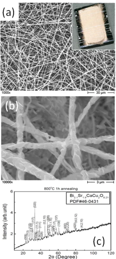
Figure1presents views of the microstructure of the non-woven nanowire networks investigated here. In (a), a SEM image with low magnification is shown, revealing the long lengths of the electrospun nanowires, and also the numerous interconnects between them. This overall structure is created during the electrospinning process, and survives all subsequent heat treatments. The inset presents a complete Bi-2212 nanowire array after the electrospinning process on a SiO2substrate.
Before the heat treatment, the sample has a white color. The dimensions are 4.74 × 6.41 mm2. Figure1(b)shows an image with high magnification (10000×). Here, the arrangement of the elon-gated, platelet-like Bi-2212 grains can be seen. The average grain size of the Bi-2212 grains is ∼37 nm. The interconnection between the individual grains is an important issue for the fabrication of conductors from this material,12and the field dependence of these contacts governs the resulting magnetic properties. Finally, Fig. 1(c)gives the x-ray data, confirming that the samples are pure Bi-2212 phase with some residing carbon.
An important issue of these nanowire networks is the determination of the superconducting volume. Fur this purpose, the weight of all samples fabricated was determined using a microbal-ance. Taking the theoretical density of Bi-2212 (6.4 g/cm3) for the individual nanowires, we find a
density of our nanowire networks of 0.0459 g/cm3.
Figure2 gives the temperature dependence of the magnetization at an applied field of 1 mT. The onset of superconductivity is found at 76.3 K, while the onset of irreversibility at this field is at about 66 K. The Tc is somewhat lower than the bulk Tcof the Bi-2212 phase (85 K), which was
also observed in Ref.11. An interesting feature is the observation that the magnetically determined critical temperature is lower than the one measured in resistance measurements on the same sam-ples,13which is opposite of bulk samples,14but seen in thin film samples.15,16Possible reasons for this behavior may be surface superconductivity or an influence of the temperature dependence of the superconducting parameters λ and ξ, which bot raise towards the critical temperature, Tc. This will
be further investigated in the future.
Figure 3 presents magnetization loops measured in fields up to ±7 T at T = 2 K, 30 K and 40 K. The magnetization loops clearly reveal the polycrystalline character of the nanowires. At low temperatures, the magnetization loops look similar to what one expects from real bulk sam-ples. At temperatures above 15 K, the loops get fully asymmetric (see the lower inset), and as a
035115-3 Koblischka et al. AIP Advances 6, 035115 (2016)
FIG. 1. (a) SEM image of the nanowire network at low magnification (1000×). The inset shows a complete, unreacted nanowire array after the electrospinning process on a SiO2 substrate. The dimensions are 4.74 × 6.41 mm2. (b) High
magnification SEM image, revealing the polycrystalline character of the nanowires and details of the elongated Bi-2212 grains. (c) X-ray analysis of the nanowire sample together with the PDF-data for Bi-2212.
035115-4 Koblischka et al. AIP Advances 6, 035115 (2016)
FIG. 2. M(T )-diagram measured in field-cooling (FC) and zero-field cooling (ZFC) in an applied field of 1 mT. The onset of superconductivity takes place at ∼76 K.
consequence, it is not possible to apply the common Bean formalism17to obtain the critical current density from the M(H) data directly. In order to solve this problem, a modelling of the entire M(H)-loop is required, which we will discuss below. Furthermore, the experimental M(H)-loops demonstrate the presence of an additional diamagnetic contribution at high temperatures and high magnetic fields, which can be expressed as MD= −KDH. The temperature dependence of this
coefficient KDis shown in the upper inset to Fig.3. The coefficient KDappears to increase fastly
with temperature that is untypical for diamagnetic atoms. There are several scenarios, e.g., one can
FIG. 3. Magnetization M as function of the applied field for temperatures ranging from 5 K to 70 K. A magnification of the center area is given in the lower inset. The upper inset shows the temperature dependence of the coefficient KD.
035115-5 Koblischka et al. AIP Advances 6, 035115 (2016)
interprete this feature as self-diamagnetism of normal cores of Abrikosov vortices. The diameter of Abrikosov vortices increases with temperature as ξ(T), where ξ is the superconductor coherence length. From this, it follows that KD(H,T) ∼ ξ(H,T)2and MDis a complex function of H.
To obtain the critical current densities from the magnetization loops, one can employ the approach of Senoussi of a three-current model,18 where the entire magnetization is composed of three contributions of the grains, the Josephson contacts between them and the shielding of the entire sample. This model can reproduce the changing shape of the measured magnetization loops, as found in an earlier publication.13A more sophisticated approach is based on an extended critical state model (ECSM) developed by Gokhfeld.19On this base, the critical current densities can be evaluated from the magnetization loops, yielding a critical current density of about 2 × 10⁷Acm−2
at 2 K, which is considerably high for this type of superconducting material.
Another important parameter of a high temperature superconductor is the temperature behavior of the irreversibility field, Hirr(T). From the M(H)-loops, Hirrwas determined directly from the
magneti-zation loops without invoking a current criterion. This procedure works well with the exception of the highest temperatures, and at low temperatures below 20 K, Hirris outside of the measurement range.
The result is presented in Fig.4. It can be seen that the irreversibility field decreases monotonously on rising temperature. The data are fitted well (red line) by the function
Hirr= A × (1 − T/Tc)3. (1)
This behavior was also observed by various authors on Bi-2223 and Bi-2212 samples.20By means of the fitting, the critical temperature is determined to be 74.4 K, corresponding to the result from the M(T) curve (see Fig.2). At temperatures below 20 K, the available magnetic field of 7 T is not strong enough to determine Hirr, and above 60 K, it is difficult to determine the closing of the loops
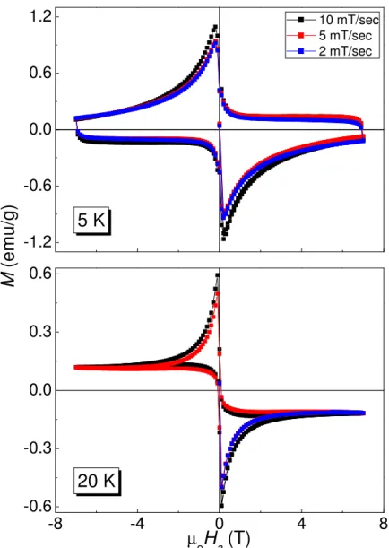
as the M(H)-data run practically parallel to each other, which is illustrated in the inset to Fig.4. Effects of flux creep and flux flow21 are other importnat characteristics of a superconducting material. Therefore, we have measured magnetization loops using various field sweep rates (dy-namic flux creep) following Ref.22. Figure5presents magnetization loops measured with various field sweep rates dB/dt= 2 mT/s, 5 mT/s and 10 mT/s at T = 5 K and 20 K. For clarity, the diamagnetic contribution was removed from the M(H)-data. One can see from the loops that the distance between the curves is largest at the zero-field peak and in the area of low fields. At high
035115-6 Koblischka et al. AIP Advances 6, 035115 (2016)
FIG. 5. M(H )-loops with different sweep rates at T = 5 K and 20 K.
fields, all three curves merge together. According to Ref.23, a dynamic relaxation rate Q can be calculated via
Q= d ln js d ln(dBe/dt)
. (2)
Of course, this procedure requires the determination of the critical current densities from the magnetization loops. A first estimation of the creep rate reveals by far less flux creep than observed on measurements of Bi-2212 single crystals23 at the same temperatures. This is due to the much higher density of grain boundaries in these nanocrystalline nanowires as compared to a well-grown single crystal. As a result, the flux pinning within the nanowires is much stronger than in single crystals, which is most important at high magnetic fields.
IV. CONCLUSION
Non-woven nanowire networks of the high-temperature superconductor Bi-2212 have been fabricated using the electrospinning technique. These nanowire networks are characterized by the
035115-7 Koblischka et al. AIP Advances 6, 035115 (2016)
long length of the nanowires, causing numerous interconnects between the individual nanowires and thus enabling the flow of supercurrents through the entire sample perimeter. The samples were characterized by means of SQUID magnetometry. The nanowires are polycrystalline with a mean grain size of about 37 nm. The nanowire networks exhibit granular hysteresis loops at temperatures above 15 K, which can only be evaluated applying a modelling of the entire loop. The temperature behavior of the irreversibility field is found to follow the same law as bulk Bi-2212 samples, but it is difficult to obtain Hirr-data at higher temperatures. Dynamic flux creep was measured on the
nanowire arrays, revealing a reduced flux creep at higher applied magnetic fields, which is due to increased flux pinning of the nanometer-sized grains.
ACKNOWLEDGMENTS
We thank Prof. V. Presser (INM Saarbrücken and Saarland University) for the possibility to use the electrospinning apparatus and Dr. D. Gokhfeld (Kirensky Institute of Physics, Krasnojarsk, Russia) for valuable discussions, Dr. J. S. Atchinson (INM Saarbrücken) and J. Schmauch (Saar-land University, group Prof. Birringer) for technical assistance. The collaboration UdS-Nancy was supported by an EU-INTERREG IVa project “Greater Region Magnetism Network (GRMN)”. This work is supported by Volkswagen Foundation.
1A. Bezryadin, C. N. Lau, and M. Tinkham, “Quantum suppression of superconductivity in ultrathin nanowires,”Nature404,
971 (2000).
2A. Bezryadin, Superconductivity in Nanowires (Wiley-VCH, 2013).
3F. Altomare and A. M. Chang, One-diemsional superconductivity in Nanowires (Wiley-VCH, 2013).
4T. R. Kline, M. L. Tian, J. G. Wang, A. Sen, M. W. H. Chan, and T. E. Mallouk, “Template-grown metallic nanowires,”
Inorganic Chemistry45, 7555 (2006).
5H. Wu, W. Pan, D. Lin, and H. Li, “Electrospinning of ceramic nanofibers: Fabrication, assembly and applications,”J. Adv.
Ceramics1, 2 (2012).
6M. Law, J. Goldberger, and P. D. Yang, “Semiconductor nanowires and nanotubes,”Ann. Rev. Mater. Res.34, 83 (2004). 7D. Li, J. T. McCann, and Y. N. Xia, “Electrospinning: A simple and versatile technique for producing ceramic nanofibers
and nanotubes,”J. Am. Ceram. Soc.89, 1861 (2006).
8J. M. Li, X. L. Zeng, A. D. Mo, and Z. A. Xu, “Fabrication of cuprate superconducting La
1.85Sr0.15CuO4nanofibers by
electrospinning and subsequent calcination in oxygen,”CrystEngComm13, 6964 (2011).
9X. L. Zeng, M. R. Koblischka, and U. Hartmann, “Synthesis and characterization of electrospun superconducting
(La,Sr)CuO4nanowires and nanoribbons,”Mat. Res. Express2, 095022 (2015).
10E. A. Duarte, N. G. Rudawski, P. A. Quintero, M. W. Meisel, and J. C. Nino, “Electrospinning of superconducting YBCO
nanowires,”Supercond. Sci. Technol.28, 015006 (2015).
11E. A. Duarte, P. A. Quintero, M. W. Meisel, and J. C. Nino, “Electrospinning synthesis of superconducting BSCCO
nanowires,”Physica C485, 109 (2013).
12F. Kametani, J. Jiang, M. Matras, D. Abraimov, E.E. Hellstrom, and D.C. Larbalestier, “Comparison of growth texture in
round Bi2Sr2CaCu2O8and flat Bi2Sr2Ca2Cu3O10wires at its relation to high critical current density development,”Sci. Rep.
5, 8285 (2015).
13M. R. Koblischka, X. L. Zeng, T. Karwoth, T. Hauet, V. Presser, and U. Hartmann, presented at EUCAS 2015,
Lyon, France, 6.9.-10.9.2015. [“Transport and magnetic measurements on Bi-2212 nanowire networks prepared via electrospinning,” IEEE Trans. Appl. Supercond (to be published)].
14M. Murakami, Melt processed high-temperature superconductors (World Scientific, Singapore, 1993).
15D. G. Naugle, “The effect of very thin Ge coating on the superconducting transition of thin Sn and Tl films,”Phys. Lett.
25A, 688 (1967).
16S. S. Tinchev, “Interface superconductivity: Possible origin of high critical temperature in layered superconductors,”Physica
C470, 626 (2010).
17C. P. Bean, “Magnetization of hard superconductors,”Phys. Rev. Lett.8, 250 (1962). 18S. Senoussi, “Review of the critical current densities and magnetic irreversibilities in high-T
csuperconductors,”J. Phys. III
France2, 1041 (1992).
19D. M. Gokhfeld, “An extended critical state model: Asymmetric magnetization loops and field dependence of the critical
current of superconductors,”Phys. Solid State56, 2380 (2014).
20M. R. Koblischka and J. Sosnowski, “Temperature-dependent scaling of pinning force data in Bi-based high-T
c
supercon-ductors,”Eur. Phys. J. B44, 277 (2005).
21Y. Yeshurun, A. P. Malozemoff, and A. Shaulov, “Magnetic relaxation in high-temperature superconductors,”Rev. Mod.
Phys.68, 911 (1996).
22M. Jirsa, L. Pust, H. G. Schnack, and R. Griessen,Physica C207, 85 (1993).
23A. J. J. van Dalen, M. R. Koblischka, and R. Grissen, “Equivalence of dynamical and conventional magnetic relaxation in