HAL Id: hal-00618207
https://hal.archives-ouvertes.fr/hal-00618207
Submitted on 1 Sep 2011
HAL is a multi-disciplinary open access archive for the deposit and dissemination of sci-entific research documents, whether they are pub-lished or not. The documents may come from teaching and research institutions in France or abroad, or from public or private research centers.
L’archive ouverte pluridisciplinaire HAL, est destinée au dépôt et à la diffusion de documents scientifiques de niveau recherche, publiés ou non, émanant des établissements d’enseignement et de recherche français ou étrangers, des laboratoires publics ou privés.
Fast propagation of weakly pinned domain walls and
current-assisted magnetization reversal in
He+-irradiated Pt/Co/Pt nanotracks
M Cormier, A Mougin, J Ferré, J-P Jamet, R Weil, J Fassbender, V Baltz, B
Rodmacq
To cite this version:
M Cormier, A Mougin, J Ferré, J-P Jamet, R Weil, et al.. Fast propagation of weakly pinned domain walls and current-assisted magnetization reversal in He+-irradiated Pt/Co/Pt nanotracks. Journal of Physics D: Applied Physics, IOP Publishing, 2011, 44 (21), pp.215002. �10.1088/0022-3727/44/21/215002�. �hal-00618207�
Fast propagation of weakly-pinned domain walls and
current-assisted magnetization reversal in
He
+-irradiated Pt/Co/Pt nanotracks
M Cormier1,2‡, A Mougin1, J Ferr´e1, J-P Jamet1, R Weil1, J Fassbender3, V Baltz4 and B Rodmacq4
1Laboratoire de Physique des Solides, Univ. Paris-Sud, CNRS, UMR 8502, F-91405 Orsay Cedex, France
2ALTIS Semiconductor, 224 Bd John Kennedy, F-91105 Corbeil-Essonnes Cedex, France
3Helmholtz-Zentrum Dresden-Rossendorf e.V., Institute of Ion Beam Physics and Materials Research, P.O. Box 51 01 19, D-01314 Dresden, Germany
4SPINTEC, UMR 8191 CEA/CNRS/UJF/Grenoble INP, INAC, 17 rue des Martyrs, F-38054 Grenoble Cedex, France
E-mail: m.cormier@science.ru.nl
Abstract. Magnetic-domain-wall propagation is experimentally studied in nan-otracks etched in ultrathin Pt/Co/Pt films with out-of-plane magnetic anisotropy, where pinning has been artificially reduced by low-dose He+-irradiation. Fast domain-wall propagation is demonstrated in such tracks under low magnetic fields, not greater than the fields necessary to make a domain wall propagate in the He+-irradiated plain films before patterning. A strong further enhancement of the track-magnetization re-versal speed is obtained thanks to a Joule-heating-induced thermomagnetic effect, by applying magnetic-field and electrical-current pulses simultaneously to the track.
PACS numbers: 75.60.Ch, 75.75.-c, 61.80.Jh, 85.70.Kh
Submitted to: J. Phys. D: Appl. Phys.
‡ Present address: Radboud University Nijmegen, Institute for Molecules and Materials, NL-6525AJ Nijmegen, The Netherlands
Fast domain-wall propagation and current-assisted reversal in Pt/Co/Pt tracks 2
1. Introduction
Current developments of magnetic data storage and processing technologies make highly desirable to control fast and reproducible magnetic-domain-wall motion in narrow mag-netic tracks [1, 2], using either magmag-netic field [1, 3, 4, 5], or electrical current [2, 6, 7]. For this purpose, nanotracks defined in ultrathin magnetic films with out-of-plane anisotropy seem to be particularly interesting [8, 9]. Especially, confinement effects due to the low film thickness lead to a lowered Walker breakdown [8, 9, 10], which allows to access the so-called precessional-propagation regime under a reduced excitation. In this regime, the continuous evolution of the domain-wall micromagnetic structure during propaga-tion is expected to lead to a reduced wall pinning by the sample’s intrinsic defects. However, in most of the out-of-plane metallic nanosystems which were studied up to now, domain-wall pinning was shown to still play a predominant role, which resulted in relatively low domain-wall velocities, as compared to the ones observed in the corre-sponding plain magnetic films [4]. In this paper, we show that in an etched Pt/Co/Pt nanotrack with out-of-plane magnetic anisotropy, where pinning has been artificially reduced by He+-irradiation [11, 12], weakly-pinned domain-walls can propagate as fast
and under magnetic field as low as in the corresponding plain irradiated film. More-over, when magnetic-field and electrical-current pulses are simultaneously applied to the track, a considerably faster magnetization reversal is observed, which is due to a Joule-heating-induced thermomagnetic effect.
2. Sample preparation
Magnetic nanotracks were patterned, by a conventional process of e-beam lithography and argon-ion-beam etching, in Pt(4.5 nm) / Co(0.5 nm) / Pt(3.5 nm) films, sputter-deposited onto thermally-oxidized Si(100) / SiO2(500 nm) substrates. The as-grown
system presents a strong out-of-plane magnetic anisotropy, and reverses its magne-tization by few domain nucleations, and predominant easy domain-wall propagation [13]. Before patterning, the films were uniformly irradiated at very low doses of 4 to 5 × 10¹⁵He+cm−2, with an energy of 30 keV. This irradiation resulted in a strong reduc-tion of the out-of-plane magnetic anisotropy [11, 14], and, consequently, of the coercive and domain-wall-propagation fields [5, 14, 15]. The widths of the tracks described in the following range from 500 to 750 nm, for a typical length of 100 µm. At one end of each track (figure 1(a)), a trumpet-like enlargement was intended to enhance the domain-nucleation probability, whereas the other end has a pointed shape.
-0.5 0.0 0.5 1.0 1.5 0 50 100 150 H (O e) t (µs) (l) 0 2 4 6 8 0 20 40 60 d (µ m ) n (m) (b) (a) (c) (d) (e) (f) (g) (n) (h) (i) (j) (k) 10 µm 10-6 10-3 100 0 50 100 150 Hpr op (O e) Dt (s)
Figure 1. Magnetic-field-induced domain-wall propagation in an etched nanotrack.
(a) Optical picture of the track (510 nm-wide, patterned in a film which was previously irradiated at a dose of 4 × 10¹⁵He+cm−2). (b)-(k) Magneto-optical images of: (b) the magnetic state of the track after nucleation of a domain out of the initially-saturated state; (c)-(k) successive magnetic states obtained starting from state (b), by applying a series of identical magnetic-field pulses (≈ 150 Oe, 1 µs), whose typical shape is depicted in (l). Dark and clear areas respectively correspond to areas of the sample which were magnetically reversed, or which are still in their initial magnetic state. (m) Distance, d (+/- 0.5 µm), travelled by the wall, as a function of the number, n, of applied field pulses. (n) Apparent domain-wall-propagation field, Hprop, as a function of the field-pulse duration, ∆t, in a similar, 750 nm-wide nanotrack, patterned in a film which was irradiated at a dose of 5 × 10¹⁵He+cm−2.
3. Field-induced domain-wall propagation
Domain-wall propagation in the nanotracks was studied, at room temperature, by magneto-optical polar Kerr microscopy. The sample was excited by magnetic-field pulses (figure 1(l)) from a small inductive coil. After each pulse, a magneto-optical image was taken, and the magnetic state of the track was deduced from an image difference with the initial, magnetically-saturated state. Figures 1(b)-(k) show an example of typical experimental results. A reversed domain is nucleated near the end of the nucleation reservoir (figure 1(b)), by the first magnetic-field pulse (about 170 Oe, 1 µs). Further pulses (here about 150 Oe, 1 µs) provoke a propagation of the corresponding domain walls, until the track is entirely reversed (figure 1(k)). Propagation is very regular,
Fast domain-wall propagation and current-assisted reversal in Pt/Co/Pt tracks 4 without any apparent pinning, as can be seen in figure 1(m), where the propagation distance is shown to be directly proportional to the number of applied field pulses. The same kind of experiment was performed for different combinations of the magnetic-field-pulse amplitude and duration. Doing this, we could estimate, for each magnetic-field-pulse duration, an apparent domain-wall-propagation field, Hprop, above which a domain wall repro-ducibly propagates (figure 1(n)): for a 1 µs pulse, Hprop ≈ 120 Oe only, while a 1 Oe dc magnetic field is sufficient to make a domain wall move, which is comparable to recent results obtained in permalloy nanotracks with in-plane magnetic anisotropy [16]. It was carefully checked that when no magnetic field is applied, domain walls do not move whithin the characteristic duration of the measurements. Besides, no further do-main nucleation was observed due to propagation-field pulses, which means that the critical propagation field is much lower than the critical nucleation field. This comes along with the extremely soft magnetic properties of the films after He+-irradiation, which are obviously conserved after patterning. Moreover, the very good homogeneity of domain-wall propagation (figure 1(m)) indicates the absence of strong extrinsic pin-ning defects which could have been introduced during the patterpin-ning process, as well as a good homogeneity of the track edges.
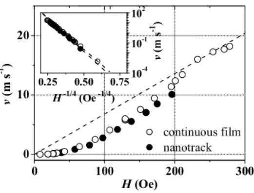
Figure 2 shows the measured domain-wall velocity, v, as a function of the applied magnetic field, H, in both an irradiated film (before patterning) and a nanotrack. So as to avoid any artifact due to transient domain-wall propagation during the rising and falling edges of the magnetic-field pulses (figure 1(l)), several measurements were performed for each field value, with different field-pulse durations. The actual “plateau” domain-wall velocity was deduced from the slope of the domain-wall-displacement vs field-pulse-duration linear dependence. Similar data measured on the as-grown film (before irradiation) can be found elsewhere [13]. The velocity curves corresponding to the irradiated film and to the nanotrack, respectively, are very similar, which is a further indication of the preservation of the irradiated-film properties after patterning. The low-field v(H) dependence is characteristic of domain-wall creep [13]. This is confirmed in the inset of figure 2, where ln v is shown to vary linearly with H−1/4, in accordance
with the creep-velocity-law of a 1D elastic interface moving in a 2D weakly-disordered medium [17, 18]: v = v0exp − Tdep T ! Hdep H !1/4 , (1)
where Tdep and Hdep are the critical depinning temperature and field, respectively, T is the measurement temperature, and v0 is a numerical prefactor. Fitting the
veloc-ity data to (1) (inset of figure 2) leads to Tdep/T ≈ 11 in the track. This is slightly higher than in the film, where Tdep/T ≈ 9, which indicates that pinning is slightly stronger in the track than in the film. This slight increase of the pinning strength in the track is coherent with previous studies of tracks similar to ours, in which artificial edge roughness was deliberately added during patterning [4]. In our tracks, pinning
Figure 2. Domain-wall-propagation velocity, v, as a function of the applied magnetic
field, H, in a plain film irradiated at a dose of 5×10¹⁵He+cm−2, and in a 750 nm-wide
nanotrack patterned in this film. The dotted line is a linear fit to the high-field velocity values in the film. Inset: Same data plotted in a coordinate system which allows to evidence the low-field creep-velocity-law (1). The dotted lines are fits to (1).
remains weak enough not to significantly perturb domain-wall propagation (figure 1). The limit field, H∗, up to which the creep-velocity-law (1) is valid, is slightly reduced in the track (60 Oe, see inset of figure 2) as compared to the film (100 Oe). Under a stronger magnetic field, domain-wall propagation rapidly becomes insensitive to pin-ning, and viscous propagation is obtained after a so-called depinning transition [13]. Unlike in the film, the viscous regime could not be clearly evidenced in the track, due to excessive nucleation under high field [19], which makes impossible to reliably measure domain-wall propagation above Hmax ≈ 200 Oe. Nucleation could not be avoided by simply reducing the duration of magnetic-field pulses, which could not be made shorter than 50 ns on our experimental setup.
After all, combining the initial properties of the magnetic films, their optimization using ion-irradiation, and a low-damage patterning process, we could reach domain-wall velocities in the tracks at least two orders of magnitude higher than those previously reported in comparable non-irradiated systems [4], while applying magnetic fields more than ten times smaller.
4. Current-assisted magnetization reversal
A further improvement in the track-magnetization reversal speed was obtained by com-bining the effects of magnetic-field and electrical-current pulses to induce reversal. Namely, we simultaneously applied a field pulse, and injected a (shorter) current pulse into a track containing domain walls (figure 3). Further details on the experimental procedure for current injection can be found elsewhere [20]. In particular, we checked that the current pulse alone did not have any effect on the domain structure in the track.
Fast domain-wall propagation and current-assisted reversal in Pt/Co/Pt tracks 6
20 µm
Figure 3. Magneto-optical images of a 750 nm-wide nanotrack, patterned in a film
irradiated at a dose of 5 × 10¹⁵ He+cm−2, before (top), and after (bottom), the
simultaneous application of a magnetic-field pulse (≈ 190 Oe, 1 µs), and an electrical-current pulse (≈ 3 × 10¹¹A m−2, 500 ns). Dark and clear areas respectively correspond
to areas of the sample which were magnetically reversed, or which are still in their initial magnetic state. The reversed domain appearing on the right in the lower picture either already existed (outside of the field-of-view) when the upper picture was taken, or was nucleated under the joint effects of field and current.
Following this procedure, a much greater track length was reversed (up to 45 µm, see left domain in figure 3) than with the same field pulse alone (10 µm, see figure 2), leading to an average track-reversal speed as high as 45 m s−1 under less than 200 Oe. For more intense current pulses (for example about 8 × 10¹¹ A m−2 during 100 ns), the entire track (about 100 µm) could even be reversed by one single field pulse. In these nanotracks, the only measurable effect of electrical current was demonstrated to be Joule heating, which totally hinders any possible spin-transfer effect [20]. Therefore, the higher reversal speed reported here is purely of thermomagnetic origin: Joule-heating during the current pulse (estimated to be about 20 K for figure 3 [21]) thermally activates magnetic-field-induced domain nucleation and domain-wall propagation, which probably both contribute to the observed reversal [19]. This situation is very similar to the process involved in laser-assisted thermomagnetic recording [22, 23].
5. Conclusion
We demonstrated that in He+-irradiated Pt/Co/Pt etched nanotracks with out-of-plane
magnetic anisotropy, considerable magnetization-reversal speeds can be obtained un-der unprecedently-weak magnetic fields. Field-induced domain-wall propagation in the tracks was shown to be as fast and under fields as low as in the corresponding non-patterned films. Taking advantage of the Joule-heating-induced thermomagnetic effect occuring when a current flows into the track, a strong further enhancement of the track-reversal speed was demonstrated. These results reflect a major improvement compared with previous results obtained in similar systems [4, 5]. They demonstrate once more the importance of ion-irradiation [5], and of a controlled and optimized patterning process [16], to achieve fast and reproducible domain wall propagation in magnetic nanotracks, known as crucial for technological applications [1, 2].
Acknowledgments
J.-P. Adam is gratefully acknowledged for assistance with the measurements. This work was partially supported by the EU-“Research Infrastructures Transnational Access” program “Center for Application of Ion Beams in Materials Research” under contract no. 025646, and by the French ANR-07-NANO-034 “Dynawall” project. M. C. thanks ALTIS Semiconductor and the French A.N.R.T. for CIFRE financial support.
References
[1] Allwood D A, Xiong G, Faulkner C C, Atkinson D, Petit D and Cowburn R P 2005 Science 309 1688–1692
[2] Parkin S S P, Hayashi M and Thomas L 2008 Science 320 190–194
[3] Beach G S D, Nistor C, Knutson C, Tsoi M and Erskine J L 2005 Nature Mater. 4 741–744 [4] Cayssol F, Ravelosona D, Chappert C, Ferr´e J and Jamet J P 2004 Phys. Rev. Lett. 92 107202 [5] Cayssol F, Men´endez J L, Ravelosona D, Chappert C, Jamet J P, Ferr´e J and Bernas H 2005 Appl.
Phys. Lett. 86 022503
[6] Thomas L and Parkin S 2007 Current induced domain-wall motion in magnetic nanowires Handbook
of Magnetism and Advanced Magnetic Materials vol 2 ed Kronm¨uller H and Parkin S (Chichester: Wiley) pp 942–982
[7] Lindner J 2010 Superlattices Microstruct. 47 497–521
[8] Jung S W, Kim W, Lee T D, Lee K J and Lee H W 2008 Appl. Phys. Lett. 92 202508
[9] Fukami S, Suzuki T, Ohshima N, Nagahara K and Ishiwata N 2008 J. Appl. Phys. 103 07E718 [10] Mougin A, Cormier M, Adam J P, Metaxas P J and Ferr´e J 2007 Europhys. Lett. 78 57007 [11] Chappert C et al 1998 Science 280 1919–1922
[12] Fassbender J, Ravelosona D and Samson Y 2004 J. Phys. D: Appl. Phys. 37 R179–R196
[13] Metaxas P J, Jamet J P, Mougin A, Cormier M, Ferr´e J, Baltz V, Rodmacq B, Dieny B and Stamps R L 2007 Phys. Rev. Lett. 99 217208
[14] Ferr´e J, Chappert C, Bernas H, Jamet J P, Meyer P, Kaitasov O, Lemerle S, Mathet V, Rousseaux F and Launois H 1999 J. Magn. Magn. Mater. 198-199 191–193
[15] Ferr´e J, Repain V, Jamet J P, Mougin A, Mathet V, Chappert C and Bernas H 2004 Phys. Status
Solidi A 201 1386–1391
[16] Malinowski G et al 2010 J. Phys. D: Appl. Phys. 43 045003
[17] Blatter G, Feigel’man M V, Geshkenbien V B, Larkin A I and Vinokur V M 1994 Rev. Mod. Phys.
66 1125–1388
[18] Chauve P, Giamarchi T and Le Doussal P 2000 Phys. Rev. B 62 6241–6267
[19] Kirilyuk A, Ferr´e J, Grolier V, Jamet J P and Renard D 1997 J. Magn. Magn. Mater. 171 45–63 [20] Cormier M, Mougin A, Ferr´e J, Thiaville A, Charpentier N, Pi´echon F, Weil R, Baltz V and
Rodmacq B 2010 Phys. Rev. B 81 024407
[21] You C Y, Sung I M and Joe B K 2006 Appl. Phys. Lett. 89 222513
[22] Mansuripur M 1995 The Physical Principles of Magneto-Optical Recording (Cambridge: Cambridge University Press)
[23] Shiroishi Y, Fukuda K, Tagawa I, Iwasaki H, Takenoiri S, Tanaka H, Mutoh H and Yoshikawa N 2009 IEEE Trans. Magn. 45 3816–3822