HAL Id: cea-01217067
https://hal-cea.archives-ouvertes.fr/cea-01217067
Submitted on 18 Oct 2015
HAL is a multi-disciplinary open access
archive for the deposit and dissemination of
sci-entific research documents, whether they are
pub-lished or not. The documents may come from
L’archive ouverte pluridisciplinaire HAL, est
destinée au dépôt et à la diffusion de documents
scientifiques de niveau recherche, publiés ou non,
émanant des établissements d’enseignement et de
Impact of storage induced outgassing organic
contamination on laser induced damage of silica optics
at 351 nm
K Bien-Aimé, C Belin, Laurent Gallais, P Grua, E Fargin, Jérôme Neauport, I
Tovena-Pecault
To cite this version:
K Bien-Aimé, C Belin, Laurent Gallais, P Grua, E Fargin, et al.. Impact of storage induced
out-gassing organic contamination on laser induced damage of silica optics at 351 nm. Optics Express,
Optical Society of America - OSA Publishing, 2009, 17, pp.18703-18713. �10.1364/OE.17.018703�.
�cea-01217067�
Impact of storage induced outgassing organic
contamination on laser induced damage of silica
optics at 351 nm
K. Bien-Aimé 1,2*, C. Belin3, L. Gallais4, P. Grua1, E. Fargin2, J. Néauport1, I. Tovena-Pecault1
1 Commissariat à l’énergie atomique, Centre d’études scientifiques et techniques d’Aquitaine, BP 2, 33114 Le Barp,
France
2 ICMCB-CNRS 87 Avenue du Docteur Albert Schweitzer 33608 PESSAC cedex, France 3
ISM-CNRS UMR 5255 351 cours de la Libération 33405 TALENCE cedex, France
4 Institut Fresnel, UMR 6133 CNRS-Universités Aix Marseille, Ecole Centrale Marseille, D.U. de Saint Jérôme,
13397 MARSEILLE cedex 20, France karelle.bien-aime@cea.fr
Abstract: The impact of storage conditions on laser induced damage
density at 351 nm on bare fused polished silica samples has been studied. Intentionally outgassing of polypropylene pieces on silica samples was done. We evidenced an important increase of laser induced damage density on contaminated samples demonstrating that storage could limit optics lifetime performances. Atomic Force Microscopy (AFM) and Gas Chromatography -Mass Spectrometry (GC-MS) have been used to identify the potential causes of this effect. It shows that a small quantity of organic contamination deposited on silica surface is responsible for this degradation. Various hypotheses are proposed to explain the damage mechanism. The more likely hypothesis is a coupling between surface defects of optics and organic contaminants.
©2009 Optical Society of America
OCIS codes: (140.3330) Lasers and laser optics: laser damage; (220.5450) Optical design and
fabrication: polishing; (110.0180); Fused silica, organic contamination, outgassing
References and links
1. M. L. André, “Status of the LMJ project,” Proc. SPIE 3047, 38–42 (1996).
2. W. H. Lowdermilk, “Status of the National Ignition Facility project,” Proc. SPIE 3047, 16–37 (1996). 3. H. Bercegol, A. Boscheron, J.-M. Di-Nicola, E. Journot, L. Lamaignère, J. Néauport, and G. Razé, “Laser damage
phenomena relevant to the design and operation of an ICF laser driver,” J. Phys. Conf. Series 112 (2008). 4. D. W. Camp, et al., “Subsurface damage and polishing compound affect the 355 nm laser damage threshold of
fused silica surfaces,” Proc. SPIE 3244, 356–364 (1998).
5. J. Neauport, L. Lamaignere, H. Bercegol, F. Pilon, and J.-C. Birolleau, “Polishing-induced contamination of fused silica optics and laser induced damage density at 351 nm,” Opt. Express 13(25), 10163–10171 (2005). 6. R. Chow, R. Bickel, and J. Ertel, “Cleanliness validation of NIF small optics,” Proc. SPIE 4774, 19–24 (2002). 7. R. R. Kunz, D. K. Downs and V. Libermann, “Experimentation and modelling of organic photocontamination on
lithographic optics,” J. Vac. Sci. Technol. B 18(3), 1306–1313 (2000).
8. A. E. Duisterwinkel, and A. T. G. M. Bastein, “Feasibility of UV cleaning of 157nm reticles,” Microelectron. Eng. 67–68, 3–9 (2003).
9. F. E. Hovis, B. A. Shepherd, C. T. Radcliffe, and H. A. Maliborski, “Contamination damage in pulsed 1µm lasers,” Proc. SPIE 2714, 707–716 (1996).
10. C. Scurlock, “A phenomenological study of contamination enhanced laser induced damage in sealed lasers,” Proc. SPIE 5647, 86–91 (2004).
11. C. Y. Sheng, “Effect of laser-induced damage on optical windows in the presence of adhesives under simulated thermal-vacuum conditions,” Proc. SPIE 6403, 1–12 (2007).
12. L. Bruel, “Environmental effects on optical component aging,” Proc. SPIE 4932, 158–169 (2003).
13. G. Ravel, and P. Bouchut, “Long term performances of very-high laser damage resistance mirrors,” Proc. SPIE
14. G. Guéhenneux, Ph. Bouchut, M. Veillerot, A. Pereira, and I. Tovena, “Impact of outgassing organic contamination on laser-induced damage threshold of optics. Effect of laser conditioning,” Proc. SPIE 5991, 59910F (2005).
15. G. Guéhenneux, M. Veillerot, and I. Tovena, “Evaluation of the airborne molecular contamination inside the LIL,” Nucl. Instrum. Methods Phys. Res. A 557(2), 676–683 (2006).
16. K. Bien-Aimé, J. Néauport, I. Tovena-Pecault, E. Fargin, C. Labrugère, C. Belin, and M. Couzi, “Laser induced damage of fused silica polished optics due to a droplet forming organic contaminant,” Appl. Opt. 48(12), 2228– 2235 (2009).
17. A. Pereira, J.-G. Coutard, S. Becker, I. Tovena, P. Bouchut, and G. Ravel, “Impact of organics contamination on 1064 nm laser induced damage threshold of dielectric mirrors,” Proc. SPIE 6403, 64030I (2006).
18. L. Lamaignère, S. Bouillet, R. Courchinoux, T. Donval, M. Josse, J.-C. Poncetta, and H. Bercegol, “An accurate, repeatable, and well characterized measurement of laser damage density of optical materials,” Rev. Sci. Instrum.
78(10), 103105 (2007).
19. P. West and N. Starostina, « AFM image artefacts», LOT-Oriel Gruppe Europa.
20. T. Pompe, A. Fery, and S. Herminghaus, “Imaging liquid structures on inhomogeneous surfaces by scanning force microscopy,” Langmuir 14(10), 2585–2588 (1998).
21. M. Commandre, and P. Roche, “Characterization of optical coatings by photothermal deflection,” Appl. Opt.
35(25), 5021–5034 (1996).
22. S. Palmier, S. Garcia, and J.-L. Rullier, “Method to characterize superficial particulate pollution and to evaluate its impact on optical components under a high power laser,” Opt. Eng. 47(8), 084203 (2008).
23. S. Palmier, J. L. Rullier, J. Capoulade, and J. Y. Natoli, “Effect of laser irradiation on silica substrate contaminated by aluminum particles,” Appl. Opt. 47(8), 1164–1170 (2008).
24. H. M. Lai, P. T. Leung, K. L. Poon, and K. Young, “Electrostrictive distortion of micrometer-sized droplet by a laser pulse,” J. Opt. Soc. Am. B 6(12), 2430–2437 (1989).
25. H. M. Lai, W. M. Suen, and K. Young, “Microscopic derivation of the force on a dielectric fluid in an electromagnetic field,” Phys. Rev. A 25(3), 1755–1763 (1982).
26. H. Bercegol, P. Grua, and J.-P. Morreeuw, “Progress in understanding of fracture related laser damage of fused silica,” Proc. SPIE 6720, 672003 (2007).
1. Introduction
High power laser facilities such as Laser MegaJoule (LMJ) [1] or National Ignition Facility [2] are currently being developed for inertial confinement fusion (ICF) experiments and for the study of matter at extreme energy densities and pressures. For the LMJ, in order to direct and amplify the 240 laser beams of 40 x 40 cm2, more than 10 000 optical components are necessary. This facility uses neodymium glass laser slabs based amplifier to deliver 20 kJ per beam at wavelength of 1053 nm. Each beam is then transported using large mirrors and subsequently frequency converted to the wavelength of 351 nm and finally focused in the center of a vacuum chamber. Maximal fluences of 25 J/cm2 are expected at 1053 nm and 14 J/cm2 at 351 nm for 3 ns pulse length. When submitted to high fluences, fused silica optics used to convey the beam after frequency conversion can exhibit localized damages that dramatically limit the optics lifetime [3]. It has been demonstrated that observed damages densities are depending on the polishing process used to manufacture the parts [4,5]. Nevertheless, molecular contamination is also suspected to be a critical issue for performances of fused silica optics. Microlithography and aerospace studies showed that airborne molecular contamination can be responsible for the degradation of optical performances. Reflective and transmissive losses have been correlated to organic contamination levels in many cases [6–8]. Moreover, in various studies, chemical contamination has been evidenced to be responsible for laser induced damage with high repetition rate laser [9–12]. In these cases, contaminants are organics such as aromatics, siloxanes derivatives and phthalates; chemical pollution is photo-deposited. A photo-induced chemical reaction increases the absorption of the film on surface and causes thermo-mechanical rupture [12]. For fusion class lasers, the problem is rather different since a few shots per day repetition rate is scheduled. Few studies have been published with such conditions [13–17]. A first study of the possible impact of organic contamination present in the environment of laser facility was previously conducted. We evidenced that the morphology of the contaminant deposited onto the surface rather than its physico-chemical nature can be responsible for the decrease of laser induced damage threshold [16,17]. In the present paper, we focus on the impact of storage conditions on the
laser induced damage density at 351 nm. To ensure an efficient replacement of the optics on the laser chain, many optical components are fabricated long before. They are stored during months in polypropylene frames put in containers. The environment confinement and the proximity of the optical components with the frame can be critical. Frames are made with polypropylene and polycarbonate materials. G. Ravel [13] showed a degradation of laser induced damage threshold at 1.06 µm for HfO2/SiO2 dielectric mirrors intentionally
contaminated by the outgassing of a polypropylene storage box. The contamination level was about a monolayer, and could not be compared with earlier works. Indeed, single shot laser impact studied by Ravel cannot be compared with laser induced damage with high repetition rate laser implying photo-induced chemical mechanism [9]. Considering Ravel results, we herein study the impact of polypropylene outgassing on laser induced damage at 351 nm of bare fused polished silica surfaces.
Our experimental protocol includes a contamination step, laser damage tests and chemical and morphological characterization of the samples; it is described in section 2. Section 3 is then devoted to results. In the last section, different damage mechanisms are studied then we conclude.
2. Experimental procedure
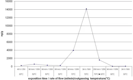
Natural polypropylene (NPP) pieces similar to the one used in LMJ optics frames were analyzed by means of ThermoDesorption-Gas Chromatography-Mass Spectrometer (TD-GS-MS) in order to determine the nature of the outgassed species. Thermodesorption of the polypropylene pieces were carried out in a specific RDT320 thermo reactor. It is a cylindrical, airtight, stainless steel chemically inert reactor with a 4.7 l capacity. The analysis is made with a Turbomass Clarus 50 chromatographer and a Perkin-Elmer mass spectrometer. The quantification and detection limit are respectively of 0.1 ng and 0.02 ng. The quantity outgassed is expressed in mass of molecules outgassed by unit of polypropylene mass. The outgassing rate of NPP is given in Fig. 1 at different temperatures, exposition times and flow rates. The outgassing temperature is scheduled during the entire exposition time corresponding to the sampling time. The flow rate of the carrier gas is set a priori in function of the temperature and the exposure time.
Fig. 1. Outgassing rate of polypropylene at different temperatures, flow rates and durations
The amount of outgassing species increases with the duration and the temperature. Maximal outgassed quantity is measured around 70°C. The outgassing rates of major
molecules measured at 70°C during 24 h and at 30°C during 48 h corresponding to the first and sixth points of Fig. 1 are given in Fig. 2.
3 48 11 0,1 0 0,4 0,1 0 0,1 0,8 0,2 0,1 1 1702 1093 386 23 179 46 21 83 0,1 0 0,1 24 10 0,4 1,4 1,8 220,9 36 6 7 15 942 341 330 0 200 400 600 800 1000 1200 1400 1600 1800 C 8 C 9 C 1 2 C 1 5 C 1 8 C 2 0 C 2 1 M IK H e x an al E th an o l, 1 -m et h o x y -, a ce ta te B en ze n ec ar b o x y li c ac id B en za ld eh y d e , 2 ,6 -d im et h y l-P h th al ic a n y d ri d e P h en o l, 2 ,6 -b is -( 1 ,1 -d im et h y le th y l) -P h e n o l, 2 ,4 ,6 ,t ri s( 1 -m et h y le th y l) -D o d e ca n o ic a ci d , p ro p y l es te r 3 ,5 -D i-te rt -b u ty l-4 -h y d ro x y p h en o n e D E P n id nid D B P n g /g 30°C 48h 70°C 24h
Fig. 2. Outgased species at 70°C during 24 h by the selected polypropylene
The detected compounds were measured during the whole duration of the outgassing cycle. The alkanes and alkenes come probably from decomposition of other higher molecules. Dibutylphthalate and diethylphthalate are esters of phthalic acid and are mainly used as plasticizers, substances added to plastics to increase their flexibility. The other molecules are measured at the beginning as well as at the end of the outgassing cycle; consequently, they probably come from NPP material and not from a surface contamination of the analyzed NPP sample. Moreover, outgassed species at 70°C and at 30°C are similar. It means that an outgassing at 70°C during 24 h can be equivalent to an outgassing at 30°C during many days which is representative of a long term outgassing such as optics storage conditions. Consequently a temperature of 70°C during 24 h was chosen for the outgassing contamination phase.
We used plano-parallel Corning 7980 fused silica polished samples. An experimental protocol detailed in Fig. 3, was used for contamination, for laser damage tests and for characterization. Preliminary, samples were cleaned using an automated cleaning procedure in a spray system machine with RBS 50 soap followed by an ethanol drag wipe. At this step, all bare samples exhibit the same laser induced damage density as typical clean LMJ optics, that is to say approximately 0.1 damage/cm2 at 351 nm, for 10 J/cm2, and 3 ns pulse length. The contamination process is then carried out in the following way: the sample to be contaminated is placed in a clean glass box with 60 g of NPP. Silica sample and NPP in the glass box are then put in an oven programmed to do a cycle consisting in a ri€sing slope of 6 h to 70°C followed by a stage of 24 h at this temperature and an abrupt return at ambient temperature during 15 min to help condensation of the outgassed species on the silica surface. To avoid any external contamination and guaranty the repeatability of the contamination process, glass box and NPP sample are cleaned in a washing machine with L51 soap followed by an ethanol cleaning prior to contamination experiment. To evaluate the impact of NPP outgassing, each contaminated sample is compared with a reference clean sample. Nevertheless, as the contaminated phase includes a heating cycle, a second reference sample is used; it is cleaned with the previous procedure and is heated with the previous temperature cycle without NPP in a similar glass box. These references were used for the following samples characterization
that are damage test, Gaz Chromatography - Mass Spectrometry (GC-MS) and Atomic Force Microscopy (AFM).
Fig. 3. Experimental protocol
The first step consists in evaluating the impact of NPP contamination on laser damage at 351 nm. A tripled Neodymium doped Yttrium Aluminum Garnet (Nd:YAG) laser was used at a wavelength of 355 nm in our laser irradiation test equipment. The spatial beam profile is Gaussian with a 1/e2 diameter of 600 µm. The pulse is a single longitudinal mode, with equivalent pulse duration τ = 2.5 ns, being defined as the ratio of total energy to peak power. The rasterscan test procedure [18] used consists of an irradiation of the substrate with a scanning step of 300 µm in order to do a complete irradiation of the defined component area. With a pulsed laser, spatial profile as well as energy fluctuates from shot to shot. As temporal profile is rather stable, we just checked that the laser goes on working with a single longitudinal mode. During the test, energy, spatial profile and beam position on the sample are recorded for each shot at 10 Hz in order to build up an accurate map of peak fluences corresponding to the scan. Then, a “postmortem” observation of irradiated areas with a long focal length working microscope at normal incidence gives a damage sites map of the sample and allows one to plot damage site density as function of peak fluence.
In order to get a better knowledge of the contamination deposited onto the silica samples two additional characterizations were conducted. Chemical analyses were performed on bare silica surface by GC-MS to determine the chemical nature of the deposited species. GC - MS analysis used a Clarus 500 Perkin Elmer equipment. It starts with ultrasound liquid extraction using a solvent composed by an iso-volume mix of 40% of methanol (CH4O, 67-56-1), 20%
of chloroform (CHCl3, 67-66-3), 20% of ethyl acetate (C4H8O2, 141-78-6) and 20% of hexane
(C6H14, 110-54-3). Both parts surfaces were sampled. The important experimental parameters
are listed in Table 1. The initial oven temperature is set at 350°C. The detection limit has been evaluated at 1.3 ng/cm2.
Table 1 Experimental parameters of GC-MS analysis
Injection temperature 350°C
Chromatographic column 5-MS (30m/0,25mm /25µm) Mass scanning 40-525 uma
At last, AFM has been used to visualize and study the morphology of the contamination layer. Imaging was performed with a Thermomicroscope autoprobe CR Research AFM.
Pictures were collected using tapping mode. A tip of 6 nm has been used. Silicon cantilevers with a force constant about 40 N/m were used with a silicon tip (NCL Nanosensor). All operations were carried out in air, at room temperature, inside a glove box, under relative humidity of 20-25%. This technique allows high resolution topographic imaging of sample surface. The tip is alternately placed in contact with the surface and then lifted off the surface to avoid dragging the tip across the surface. Tapping mode imaging is implemented by oscillating the cantilever assembly at or near the cantilever resonant frequency using piezoelectric quartz. When the tip is not in contact with the surface, the tip oscillates with high amplitude (about 80 nm) thanks to the piezo motion. During the approach step, the oscillating tip is moved toward the surface until it begins to lightly touch the surface. Then, during the scanning, the vertically oscillating tip alternately contacts the surface and lifts off at a frequency between 160 kHz and 180 kHz. The cantilever oscillation amplitude is maintained constant by a feedback loop. When the tip passes over a bump or a depression, the amplitude of oscillation decreases or increases respectively. The oscillation amplitude is measured by a detector. The oscillation amplitude variations are calculated in topographic signal thanks to numerical processing in order to identify and measure surface features. The set point is basically a measure of the force applied by the tip to the sample. In tapping mode, the set point indicates the amplitude of oscillation of the cantilever which controls the force with which the tip taps on the sample. The amplitude of oscillation is a fraction of the free amplitude which is that of the tip when there is no tip-surface interaction.
3. Results
Laser induced damage tests have been made on several clean, heated, and contaminated silica samples. The total surface tested is about 100 cm2 for each type of sample. Results are presented on Fig. 4. Firstly, damage tests reveal that clean and heated samples are similar. It demonstrates that the outgassing protocol without NPP has no effect on damage density. Laser damage tests on clean sample did not generate damage at fluences below 14 J/cm2. Secondly, the impact of NPP outgassing is significant. Indeed, from 11 J/cm2 to 14 J/cm2, damage density is increased by a factor of 5 to 200 on contaminated samples.
0,1 1 10 100 1000 10000 8 9 10 11 12 13 14 15 16 17 18 Fluence (J/cm²) D a m a g e d en si ty
Clean Heated Contaminated
Fig. 4. Laser induced damage tests of clean, heated and contaminated silica samples
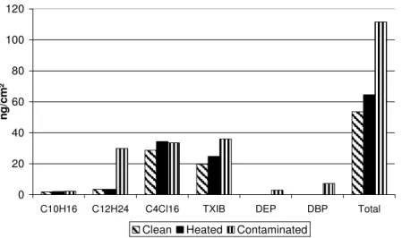
GC-MS analyses were performed to identify the nature of sample surface contaminants. Results are presented on Fig. 5.
0 20 40 60 80 100 120
C10H16 C12H24 C4Cl16 TXIB DEP DBP Total
n
g
/c
m
²
Clean Heated Contaminated
Fig. 5. Chemical species measured by GC-MS on clean, heated and contaminated silica samples
The amount of each molecule measured is expressed in terms of mass per unit surface. Comparison of clean, heated and contaminated samples demonstrates that contamination carried out with NPP increased global amount of contaminant by a factor of 2. NPP contamination induces an additional contamination of diethyphthalate (DEP), dibutylphthalate (DBP) and C12H24. Additional GC-MS measures on contaminated samples confirmed this
increase of a factor 2 compared with clean or heated sample. Other condensable molecules were found; which demonstrated that this mode of contamination generate a mixture of various condensable molecules on silica surfaces.
AFM measurements were made to determine the morphology of the contaminant layer. The measurements after cleaning and after contamination with NPP were compared. The same areas were analyzed each time. After cleaning, as shown on Fig. 6a, all samples exhibit a root mean square roughness of 0.1 nm with a standard deviation of 0.01 nm; which is conform to manufacturer’s roughness specifications. Then, we performed the same measures after contamination. As showed on Fig. 6b, on the contaminated sample, streaks appear on the picture. AFM manufacturers warn that these streaks are artifacts related to a tip contamination [19]. They appear especially in location where there are sharp features and edges on the sample surface such as scratches or digs.
Fig. 6. AFM picture of bare silica samples after cleaning (a) and after contamination (b) – solvent spread on a fused silica sample (c)
These artifacts are relevant of a tip problem; the tip can be charged with liquid when scanned over the surface. To be sure that these artifacts are linked to the presence of liquid on the surface, a surface with a droplet of solvent deliberately deposited on it with a micro syringe, was measured. As shown on Fig. 6c, the presence of many streaks demonstrates that this behaviour of the tip is linked with the existence of a liquid film. Nevertheless, as this kind
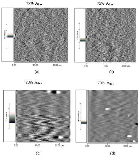
of pictures can also be attributed to the fact that the approach of the tip is not effective, complementary experiments were performed. AFM images of clean silica samples and contaminated ones were made with different set point amplitude values (Fig. 7). For 79% or 73% of the free amplitude, respectively images a and b of Fig. 7, clean bare silica surface is well distinguishable. We found the same root mean square roughness certified by the manufacturer. On contaminated samples, for low forces (80% of the free amplitude, Fig. 7c) the tip generates streaks and for higher force (70% of the free amplitude, Fig. 7d), the silica surface is still not apparent. Indeed, at the end of the measure, after the withdrawal step, the natural oscillating amplitude of the tip has decreased of about 20 nm and a shift of natural frequency was noticed. In normal conditions, the natural oscillating amplitude and frequency come back to the ordered values at the end of the withdrawal.
Fig. 7. AFM picture of bare silica samples after cleaning (a and b) and after contamination (c and d) for different set point amplitude values
In a similar experiment, imaging droplets, Pompe [20] noticed various behaviors for trace and retrace signal as well as amplitude and resonance frequency shifts of the cantilever, depending on the chosen set point amplitude value. It was attributed to the instability of the cantilever motion against the attractive capillary forces. For small set point, a permanent liquid bridge between the tip and the liquid drop is formed. This liquid bridge is likely to alter our AFM measurements.
The combination of all these AFM experimental data evidences that streaks artifacts are due to the presence of liquid on the surface. These streaks could be on the entire AFM picture
or only on an area of the image, showing that the liquid contamination could be spread as a film or as microscopic droplets on the surface. These two kinds of morphology could be found on a single sample with no peculiar organization. The nature of molecules was given by GC-MS analysis and shows that this contamination is a mixture of several organic condensable molecules. The question that arises now is how the NPP contamination induced by contaminants present in form of a liquid film or droplets on the surface can drastically increase damage density.
4. Discussion
Different damage mechanisms were proposed. Firstly, the possibility of a thermomechanical rupture induced by the absorption of the laser beam was studied. Based on AFM study, two different morphologies were considered; film and micrometer sized droplets were differentiated.
Firstly, a film contaminant configuration was considered. Chemical analysis of the NPP contamination gives rise to the presence of diverse organic molecules. Considering the major molecules measured by GC-MS, that is to say dibutylphthalate, diethylphthalate, and 2,2,4-trimethyl-1,3-pentanediol diisobutyrate, their absorption coefficient α, measured by UV spectrophotometry, were found to be lower than 0.02 cm−1. Thereby, absorption calculations were made considering each molecule separately. A thermally isolated contaminant layer of thickness e with αe<<1 are taken into account. The heating of the film is given by the equation: p F T C α ρ ∆ = (1)
where F is the fluence, Cp is the film’s specific heat, and ρ is the film’s density. For the
considered molecules and a pulse fluence of 15 J/cm2, the temperature rise is less than 1°K. Additionally, photothermal deflection measurements were performed. This technique is currently used to quantify the absorption of optical component or thin film. The sample under test is heated with an intensity modulated pump laser beam. Resulting from the optical absorption of the intensity modulated pump beam, a local temperature rise occurs and a thermal wave propagates in the structure. This modulated temperature generates spatial refractive-index variations. Photothermal deflection measures the deflection of the probe beam due to the refractive index gradients. One can obtain the absorption value on the conditions that a proper calibration has been performed. This technique permits accurate measurements of absorption losses as low as 10−6. The experimental setup was already presented elsewhere [21]. Our experimental setup uses a pump continuous Argon ion laser with a mid-UV multiple output (333.6 nm-363.8 nm). This beam laser is directed so that the angle of incidence on the sample surface will be approximately 15° with respect to the normal with s polarization. It is modulated by an optical chopper at a frequency of 1200 Hz. The incident power on the sample is 1 W for a beam diameter of 15 µm. The probe laser is a 0.8 mW helium–neon laser at 633 nm, which is directed at 15° with respect to the normal. The linearity of the signal with incident power has been checked assuring that linear absorption was measured. Moreover, the reproducibility has been tested by measuring successively the same area certifying that the sample had not been modified by the measurement.
The measurements were made on various areas of the sample and two times for each kind of sample. The same result has been found each time, which indicate that the signal is independent of the liquid contamination morphology. An example of experimental measurement results is given in Fig. 8
Fig. 8. Absorption mapping of clean (a) and contaminated (b) samples obtained by photothermal deflection with a sampling step of 20 µm
For the clean sample, a mean value of 2.93 10−5 with a standard deviation of 4.08 10−6 was measured; for the contaminated sample, a mean value of 1.95 10−5 with a standard deviation of 9.43 10−6 was measured. The difference between the clean and the contaminated sample is not significant showing that contamination does not affect absorption mappings. This technique is not adapted to measure such absorption. Furthermore, the more absorbing points visible are due to micrometer sized particles on the sample. We must outline that Palmier demonstrated that particles cannot be linked to damage in similar conditions (polished fused silica samples damage tested at 351 nm) [22,23].
Considering that organic is condensed as micro-droplets that are thermally isolated, the equation of the evolution of temperature in an inclusion is given by the equation:
v T C S t ∂ = ∂ (2)
where Cv is the volume specific heat, S the power density.
The power density S depends on the absorption cross section σabs, the radius a of the
droplet and the laser intensity I0, it is given by the equation:
0 3 ( ) ( ) 4 3 absI t S t a σ π = (3)
The absorption cross section σabs is given by the formula
3 2 2 2 2 2 1 2 1 ' . '' 6 2 1 abs n n a c n n n ω σ = π + (4)
where n1 is the real part of the complex refractive index of the environmental medium, n2’ and
n2” are respectively the real and the imaginary parts of the complex refractive index of the
contaminant. The temperature rise calculated for each organic contaminant measured and for a pulse fluence of 15 J/cm2 is less than 0.2 K. Then, whatever the morphology of contamination condensed, the temperature increase is insufficient to create a mechanical rupture. Consequently, second hypothesis has been studied.
Our previous study [16] showed that by a micro-lens effect, microscopic droplets can also be responsible for the decrease of laser induced damage threshold of fused polished silica optics. Based on these previous results, we wondered if an electrostrictive force could cause a displacement of our organic contamination during the rasterscan procedure thus forming a droplet. In this hypothesis, for a given film’s morphology, the aim is to calculate if the
electrostrictive force can induce sufficient displacement to create a microscopic droplet likely to produce a lens effect. Lai completed several works [21–25] on the electrostrictive distortion of micrometer sized droplets by a laser pulsed. Considering a film’s morphology, calculations were made with the same formalism as Lai. The displacement induced in these conditions is calculated to be of a few picometers for all organic molecules measured. It is therefore impossible to form a micro droplet that could create damage as seen in [16].
5. Conclusion
We study the impact of organic molecular contamination on single shot laser induced damage density at the wavelength of 351 nm, 3 ns pulse length. Experiments with deliberated contamination were made with polypropylene material, on the surface of bare fused silica polished samples. Important increase of laser induced damage density was observed compared to reference sample with a degradation of up to two decades. We coupled chemical ultra-trace surface analysis and AFM measures to identify the organic contaminated layer. To explain the damage mechanism, different hypotheses have been studied. Calculations demonstrated that thermomechanical rupture because of an increase of the absorption due to the organic film was not possible. Moreover, the second hypothesis studied concerns the electrostrictive behaviour of the film generating a micro-lenses that creates focusing effect. Nevertheless, electrostrictive forces were insufficient to create such droplets. Since simple mechanisms based on direct absorption by contaminants must be avoided on the basis of previous considerations, investigation of the physical mechanisms responsible of laser damage density increase after organic contamination is ongoing. That concerns especially the role of submicroscopic droplets, from two points of view. The first is related with laser electric field enhancement induced by droplets deposited on the optics surface, occurring over a depth of the order of a micrometer for submicroscopic droplets. Thus, since subsurface cracks in fused silica optics have been demonstrated to be possible damage initiators at 351 nm [26], the field enhancement mechanisms may lead to a possible coupling effect between subsurface damage and organic contamination. The second point of view is about droplet distortion induced by the laser wave. Lai [21–25] has shown laser induced distortion of 50 µm water droplets at an intensity of 1.5 GW/cm2, for a 0.60 µm wavelength and a pulse duration of 0.4 µs. In our case, rasterscan irradiations are made with a 355 nm laser beam at an intensity of 6 GW/cm2, and a 2.5 ns pulse duration. For such laser irradiations, significant distortions of submicroscopic droplets may be expected, subsequently able to create strong field enhancements within organic material, which could allow non linear absorption. This topic is the object of further studies.
Acknowledgements
The authors would like to thank L. Lamaignère, T. Donval, M. Loiseau from CEA for laser damages tests as well as TERA environnement company for GC-MS results. We also sincerely thank H. Bercegol for valuable discussions.