HAL Id: hal-03002316
https://hal.archives-ouvertes.fr/hal-03002316
Submitted on 12 Nov 2020
HAL is a multi-disciplinary open access
archive for the deposit and dissemination of
sci-entific research documents, whether they are
pub-lished or not. The documents may come from
teaching and research institutions in France or
abroad, or from public or private research centers.
L’archive ouverte pluridisciplinaire HAL, est
destinée au dépôt et à la diffusion de documents
scientifiques de niveau recherche, publiés ou non,
émanant des établissements d’enseignement et de
recherche français ou étrangers, des laboratoires
publics ou privés.
Behavior of space charge in polyimide and the influence
on power semiconductor device reliability
Kunihiko Tajiri, Hirotaka Muto, Didier Marty-Dessus, Laurent Berquez, G.
Teyssedre, Marie-Laure Locatelli, Sombel Diaham, Virginie Griseri, Flora
Carrasco
To cite this version:
Kunihiko Tajiri, Hirotaka Muto, Didier Marty-Dessus, Laurent Berquez, G. Teyssedre, et al.. Behavior
of space charge in polyimide and the influence on power semiconductor device reliability. Polyimide
for electronic and electrical engineering applications, InTechOpen Editor, 2020, 978-1-83880-098-7.
�hal-03002316�
Behavior of space charge in polyimide and the
influence on power semiconductor device reliability.
Kunihiko Tajiri, Hirotaka Muto, Mitsubishi Electric Corporation, Amagasaki, Hyogo, Japan,
Didier Marty-Dessus, Laurent Berquez, Gilbert Teyssedre, Marie-Laure Locatelli, Sombel Diaham, Virginie Griseri, Flora Carrasco, LAPLACE, Université de
Toulouse, CNRS, INPT, UPS, Toulouse, France,
Abstract. Polyimide is widely used in film form as a passivation material for power
semiconductor devices such as Si, SiC, GaN, etc. The magnitude of the electric field at the edge termination area of these semiconductor devices is becoming higher due to the increase of operational voltage and/or demand for shrinking the edge termination area to increase device active area. Hence it is concerned that the accumulation of space charge in the encapsulation and passivation material may affect the insulation performance of these devices, for example, the degradation of withstand voltage due to distortion of the internal electric field caused by space charge accumulation. To design space charge resistance of semiconductor devices, it is important to understand the space charge behavior in polyimide films with a thickness of several to several tens of µm. This chapter addresses practical implementation, specifications and issues on space charge in polyimide insulation on power semiconductor devices focusing on the space charge measurements in thin polyimide films using the latest developed LIMM method and DC conductivity measurements.
Keywords: passivation material, space charge, LIMM, DC conductivity, power
semiconductor device
1. Introduction
In recent years, high voltage electronics and power electronics applications have emerged needing the use of power semiconductor devices with widely used Si and wide bandgap materials such as SiC, GaN. In these devices, thin polymer material have been widely used as passivation coating to protect device surfaces. Particularly, polyimide (PI) is of great interest due to its excellent thermal and electrical properties and its easy processing. Some of the most important applications of these materials films are as inter-level dielectric insulators and as electronic device surface passivation [1]. The typical image of PI layer at the edge surface of semiconductor chip is shown in Figure 1.
Figure 1. Power module and edge termination structure of semiconductor chip
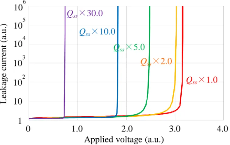
Space charge is generally reported as a triggering mechanism for the degradation of insulators [2], and considered as a cause of the decrease of electrical breakdown voltage of those polymer films. Furthermore, the space charge could degrade semiconductor leakage current characteristics by strengthening the electric field in semiconductor substrate region. The influence of space charge transportation and accumulation on surface of semiconductor chip has been discussed in [3][4][5][6] using TCAD simulation. Reliability tests of IGBT devices under accelerated conditions were reported in [7][8] showing that the degradation (increase) of leakage current of the device is caused possibly by the formation of space charge on the surface at semiconductor edge termination area. The decrease of withstand voltage of HV IGBT due to accumulated space charge (Qss) on the surface of device edge termination area has been demonstrated
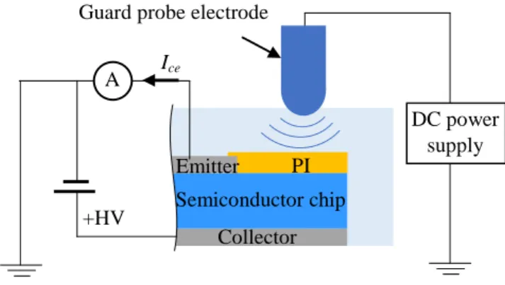
by TCAD simulation as shown in Figure 2. Attempts have also been made to evaluate the space charge resistance of a real chip by evaluating the withstand voltage of a semiconductor chip using a guard probe electrode to simulate an external electric field due to space charge as shown in Figure 3 [9].
Figure 2. Avalanche voltage simulation results of HVIGBT chip for different Qss
0 1.0 2.0 3.0 4.0 Applied voltage (a.u.)
L ea k ag e cu rr en t ( a. u .) 10 1 104 105 106 103 102 Qss×1.0 Qss×2.0 Qss×5.0 Qss×10.0 Qss×30.0 PI Collector Semiconductor chip +HV Emitter Encapsulation
(a) HV IGBT power module (b) Edge termination structure of semiconductor chip
Figure 3. Schematic view of guard probe (GP) method and leakage current dependent on the guard prove voltage
To evaluate the actual influence by the space charge accumulation, it is necessary to clarify the space charge distribution around the edge termination area of semiconductor chip. Many trials have been performed to measure the space charge characteristics in polyimide and encapsulation material such as silicone gel as described below. Earlier reports featuring space charge in PI [10
–
12] reported the processes indirectly e.g. through charging current measurements or directly as with pulsed electroacoustic (PEA) method with relatively thick films (125 µm) [10]. In [10], the effect of humidity in air and difference due to electrode material (Al and Au) on space charge formation with time evolution are discussed.Recently, the Laser Intensity Modulation Method (LIMM) [13] have been performed to investigate space charge characteristics in thin PI films with few µm in thickness under the DC field up to 125 kV/mm, close to breakdown voltage [14
–
17]. In [17], the space charge characteristics were reported under DC voltage of from low field of 2.5 to 125 kV/mm with the correlation with DC conductivity trends. Considering the encapsulation material, some studies have been performed through charge accumulation measurement in silicone gel by using PEA [18][19] and LIPP (Laser-Induced Pressure Pulse) [20] methods, and space charge characteristics of only surface information and total amount of charge have been measured in [18][19] and [20], respectively.As described, many attempts have been made to evaluate the influence of space charge, quantitative evaluation has been under development, especially in thin PI.
L ea k ag e cu rr en t Ice ( a. u .) 0 1.0 2.0 3.0 4.0 5.0 6.0 7.0 Applied voltage Vce (a.u.)
10 1 102 103 104 0V -1.0kV -1.5kV -2.0kV -2.5kV -3.0kV -3.5kV -4.0kV Guard prove voltage Semiconductor chip
Guard probe electrode
A Ice
+HV
DC power supply
(a) Schematic view of guard probe method
(b) Leakage current of semiconductor chip Collector
However, the space charge distribution in the PI film, which is important for providing space charge tolerance of semiconductor chip, is gradually becoming apparent along with the influence of the operating environment. In this chapter, the latest developments with space charge measurements in thin polyimide films using the LIMM method, with the focus on local field strengthening and correlation with conductivity measurements.
2. Space charge evaluation methods
2.1 PEA method
Since the 1980s, the PEA method has been used to measure the space charge of sheet or film samples in order to investigate space charge phenomena and evaluate the aging of dielectrics. A space charge distribution by converting a pressure wave generated by applying a pulse electric field to a sample under high voltage application, and converting the pressure wave into an electric signal using a piezoelectric element. The thickness of the sample that can be evaluated by PEA is more than 100 µm and its spatial resolution is about several tens of µm.
2.2 (F)LIMM method
The (Focused) Laser Intensity Modulation Method or (F)LIMM is a thermal wave method dedicated to the space charge analysis of thin dielectric films (with a thickness from 5 μm to 50 μm) [21, 22]. This method is originally proposed by Lang [23] in the 1980s, and the characterization of space charge distribution had been performed under volt-off after external DC voltage application. Recent development has been reported that LIMM measurement is carried out under volt-on [24]. The LIMM is much suitable to clarify the space charge characteristics in a polymer film with only several μm thickness, which is a typical thickness of passivation layer on a semiconductor chip. Figure 4 shows the schematic diagram of On-line LIMM. A DC potential (Vht) is applied to the top electrode of the measuring cell through a
low-pass filter. (F)LIMM currents are recorded after pre-amplification and extracted from noise by a lock-in amplifier. To protect a damage from an eventual breakdown of the sample, an electrical protection device was introduced at the output of the measuring cell.
The thermal gradient created by the laser beam induces periodical and local expansions that lead to relative charge displacement regarding to the electrodes within the irradiated volume. Varying the laser beam modulation frequency, one can control the depth of thermal diffusion and then calculate its effect on the total current signal. Finally, a mathematical treatment allows charge density profiles reconstruction in the direction of the sample thickness. A modulated laser beam of a frequency f heating a surface S of a top electrode sputtered on a dielectric non-polar sample of thickness L, to which an additional DC voltage Vht is applied, the
fundamental (F)LIMM equation for the complex current I(f) can be expressed by [24]:
(1)
z is the direction normal to the sample, αz the coefficient of thermal expansion (K-1), αε
the coefficient of thermal dependence of the dielectric permittivity (K-1), the permittivity, Ei(z) the internal electric field along z-axis (V.m-1) and T(z,f) the simulated
spatial variation of the temperature versus frequency.
3. Space charge behavior in polyimide film
3.1 Space charge distribution in polyimide film
In this subsection, the LIMM measurement results of PI film in a typical case using cumulative DC voltage application. Figure 5 shows the sample structure and the example of LIMM measurement protocol. The thickness of PI film is 20 μm. The polarization steps consist in applying a DC electric field from 25 to 125 kV/mm with positive or negative polarity. The corresponding positive or negative DC voltages are applied on the top electrode of the sample in air at room temperature, whereas the Si substrate is grounded. After each polarization step, a depolarization process is performed by short-circuiting the sample. A cumulative protocol is applied for successive voltage steps on the sample as shown in the right side of Figure 5. Volt-on and volt-off steps of each 60 min are applied on the sample from 25 to 125 kV/mm, with the steps of 25 kV/mm. LIMM measurements are performed throughout the whole protocol, with every 10 min scanning of 63 frequency points from 10 Hz to 10 kHz.
Figure 6 shows LIMM current waveform under the field of 25, 50, 75, 100, and 125 kV/mm, positive polarity. The space charge and internal electric field distributions are deduced from Eq. (1) as shown in Figure 7 (a) and (b), respectively. In this case, positive and negative space charges are confirmed close to and at the depth of from 4-10 µm from top Au electrode, respectively, which causes the enhancement of positive field strengthening at 2-6 µm depth. The maximum values of these are confirmed to increase along with the applied DC field. Time evolution of maximum peaks of enhanced electric field in both polarities are shown in Figure 8. As mentioned so far in this subsection, the space charge and enhanced electric field characteristics in polyimide under external DC voltage on and off can be evaluated including depth-profile, time evolution, as will be explained in subsection 3.2, can be evaluated by using LIMM method.
Figure 5. Typical sample structure and LIMM measurement protocol (cumulative voltage application of 25-125 kV/mm, positive polarity)
Figure 6. Example of LIMM current waveform (25-125 kV/mm, positive polarity) Frequency (Hz) L IMM cu rr en t (p A) 10 102 103 104 10 5 0 -5 -10 -15 25 kV/mm, real 25 kV/mm, imag. 50 kV/mm, real 50 kV/mm, imag. 75 kV/mm, real 75 kV/mm, imag. 100 kV/mm, real 100 kV/mm, imag. 125 kV/mm, real 125 kV/mm, imag. Au PI NiSi Si substrate (n-type) HV (positive or negative) GND Ap p lied elec tr ic field ( k V/m m ) 0 1.0 2.0 3.0 4.0 5.0 6.0 7.0 8.0 9.0 10.0 Time (hr) 125 0 75 50 100 25
(b) LIMM measurement protocol (a) Sample structure
Figure 7. Example of the depth profiles of (a) space charge and (b) internal electric field (25-125 kV/mm, positive polarity)
Figure 8. Magnitude of positive peaks of internal electric field
E lectr ic field ( k V/m m ) 75 25 0 100 Positive polarity Negative polarity Applied electric field 150 0 1.0 2.0 3.0 4.0 5.0 6.0 7.0 8.0 9.0 10.0 11.0 Time (hr) 125 50 C h ar g e d en sity ( C /m 3 ) 500 0 -500 Depth (m) 0 2 4 6 8 10 12 14 16 18 20 (a) (b) In ter n al e lectr ic field ( k V/m m ) 40 20 0 60 -20 -40 -60 80 1,000 1,500 2,000 2,500 Depth (m) 0 2 4 6 8 10 12 14 16 18 20 25 kV/mm 50 kV/mm 75 kV/mm 100 kV/mm 125 kV/mm 25 kV/mm 50 kV/mm 75 kV/mm 100 kV/mm 125 kV/mm Positive charge increases. Negative charge peak increases.
Positive field peak increases.
3.2 DC conductivity
To clarify the influence of space charge accumulation to the conductivity behavior, space charge density and internal electric field are compared with DC conductivity. Figure 9, 10, and 11 show the maximum space charge density of negative charge, maximum positive internal electric field, and DC conductivity, respectively, under the applied field from 25 to 125 kV/mm for both polarities. To compare these figures, no remarkable influence on the conductivity by space charge accumulation inside polyimide at this level work. To establish a direct link between space charge dynamics and conduction phenomena, further evaluations are still necessary.
Figure 9. Maximum negative space charge density
Figure 10. Maximum positive internal electric field 100
-150 -100 -50 0 50 100 150 Applied electric field (kV/mm)
60 40 0 Ma x im u m in ter n al elec tr ic field ( k V/m m ) 80 20 Positive polarity Negative polarity Ma x im u m s p ac e ch ar g e d en sity ( C /m 3 ) 0 -150 -100 -50 0 50 100 150 Applied electric field (kV/mm)
-100 -300 -500 -200 -400 Positive polarity Negative polarity -600 -700
Figure 11. DC conductivity
4. Effect of space charge on semiconductor devices
As describe in Section 1, the degradation (increase) of leakage current of the device is caused possibly by the formation of space charge on the surface at semiconductor edge termination area. Figure 10 shows the electric field enhancement ratio defined in Eq. (2) confirmed in the LIMM measurement depending on the applied DC field of from -25 to 25 kV/mm. It is confirmed that the enhancement ratio in PI film is negligibly small (less than 1.1) for applied fields less than 10 kV/mm. However, it can reach much higher like 1.4 at higher applied field like 25 kV/mm.
Figure 10. Peak value of internal electric field linked to field strengthening (filled circle) and enhancement ratio of those peaks (open square) versus applied electric
field (2) 0 12 10 8
Applied electric field (kV/mm) 6 4 2 -30 -20 -10 0 10 20 30 In ter n al elec tr ic field ( k V/m m ) E n h an ce m en t r atio 1.0 1.8 1.6 1.4 1.2 Internal electric field
Enhancement ratio DC co n d u ctiv ity ( S/c
m) Negative polarity Positive polarity 10-15
-150 -100 -50 0 50 100 150 Applied electric field (kV/mm)
10-16
10-17
This result implies that electric field at edge termination area should be carefully designed under such an operational electric field as is the case of SiC devices to prevent the influence of space charge accumulation. It should be noted that not only inside polyimide, but space charge accumulations in encapsulation material and the interface between polyimide and encapsulation as its structure shown in Figure 1 are also needed to be clarified. Moreover, the influence of environmental conditions such as temperature and humidity on the space charge behavior should be taken into account.
Conclusion
It has been presented that the space charge distribution can be clarified in thin polyimide film using LIMM method from relatively low field of 2.5 kV/mm up to 125 kV/mm which is close to breakdown field. The electric field enhancement due to space charge accumulation is shown to be 1.4 times at 25 kV/mm under room temperature condition. To design much reliable structure against space charge accumulation in polyimide and encapsulation material, its distributions are needed to be clarified by the further study.
Acknowledgments
The authors would like to express our gratitude to all the people who have involved in this work, especially, Dr. Thierry Lebey who is former Director of LAPLACE for his tremendous support during the collaborative research about LIMM evaluation.
References
[1] S. Zelmat, M.-L. Locatelli, T. Lebey, and S. Diaham, “Investigations on high temperature polyimide potentialities for silicon carbide power device passivation”, Microelectronic Engineering vol. 83, pp. 51-54, 2006. DOI: 10.1016/j.mee.2005.10.050
[2] G. Mazzanti, G. C. Montanari, and L. A. Dissado, “Electrical aging and life models: the role of space charge”, IEEE Transactions on Dielectrics and Electrical Insulation vol. 12, pp. 876-890, 2005. DOI: 10.1109/TDEI.2005.1522183
[3] M. Rahimo et al., “The impact on power semiconductor device operation due to local electric field alterations in the planer junction termination” Microelectronics Reliability vol.58, pp.51–57, 2016. DOI: 10.1016/j.microrel.2015.12.021
[4] I. Imperiale et al., “TCAD Modeling of Charge Transport in HV-IC Encapsulation Materials”, Proceedings of the 26th International Symposium on Power Semiconductor Devices & IC's, 15-19 June, 2014, Waikoloa, Hawaii, USA. DOI: 10.1109/ISPSD.2014.6856073
[5] I. Imperiale et al., “TCAD modeling of encapsulation layer in voltage, high-temperature operation regime”, Proceedings of 44th European Solid State Device Research Conference (ESSDERC 2014), 22-26 September 2014, Venice, Italy. DOI: 10.1109/ESSDERC.2014.6948826
[6] I. Imperiale et al., “Role of Encapsulation Formulation on Charge Transport Phenomena and HV Device Instability”, Proceedings of IEEE 65th Electronic Components and Technology Conference (ECTC 2015), 26-29 May 2015, San Diego, CA, USA. DOI: 10.1109/ECTC.2015.7159586
[7] N. Tanaka et al., “Robust HVIGBT module design against high humidity”, in Proceedings of Power Conversion and Intelligent Motion (PCIM) Europe 2015, pp. 368-373, 2015. 19-21 May 2015, Nuremberg, Germany. ISBN: 978-3-8007-3924-0
[8] Y. Kitajima et al., “Lifetime estimation model of HVIGBT considering humidity”, Proceedings of Power Conversion and Intelligent Motion (PCIM) Europe 2017, pp. 353-358, 2017. Nuremberg, Germany. ISBN: 978-3-8007-4424-4
[9] A. Yamatake et al., “New Technology for Evaluating Insulation Reliability of Termination of Power Semiconductor Chip”, Proceedings of the IEEJ Transactions on Electrical and Electronic Engineering 2017, p. 157, 19-20 September 2017, Muroran, Hokkaido, Japan.
[10] K. Kaneko, R. Shiomi, Y. Suzuoki, T. Mizutani, H. Shiota, and H. Muto, “Effects of electrode material on injection and space charge formation in polyimide”, Proceedings of IEEE International Conference on Solid Dielectrics, pp. 518-521, 2007. DOI: 10.1109/ICSD.2007.4290865
[11] G. M. Sessler, B. Hahn, and D. Y. Yoon, “Electrical conduction in polyimide films”, Journal of Applied Physics, vol. 60, pp. 318‑326, 1986. DOI: 10.1063/1.337646
[12] T. Liang, Y. Makita, and S. Kimura, “Effect of film thickness on the electrical properties of polyimide thin films”, Polymer, vol. 42, pp. 4867-4872, 2001. DOI: 10.1016/S0032-3861(00)00881-8
[13] A. Petre, D. Marty-Dessus, L. Berquez, and J.-L. Franceschi, “A comparison of different mathematical treatments for solving the inverse problem in focused laser intensity modulation method”, Japanese Journal of Applied Physics, vol. 43, pp. 2572-2579, 2004. DOI: 10.1143/JJAP.43.2572
[14] M.-L. Locatelli, C. D. Pham, S. Diaham, L. Berquez, D. Marty-Dessus, et G. Teyssedre, “Space charge formation in polyimide films and polyimide/SiO2 double-layer measured by LIMM”, IEEE Transactions on Dielectrics and Electrical Insulation, vol. 24, no 2, pp. 1220-1228, April, 2017. DOI: 10.1109/TDEI.2017.006172
[15] F. Carrasco et al., “Assessment of the High Field Behaviour of Polyimide Films: Experimental Methods and Impact of Electrode Material”, Proceedings of the International Symposium on Electrical Insulating Materials 2017 (ISEIM 2017), pp. 122-125, 11-15 September 2017, Toyohashi, Aichi, Japan. DOI: 10.23919/ISEIM.2017.8088704
[16] F. Carrasco et al., “Effect of film thickness and electrode material on space charge formation and conductivity in polyimide films”, Proceedings of the IEEE International Workshop on Integrated Power Packaging 2019 (IWIPP 2019), 24-26 April 2019, Toulouse, Haute-Garonne, France.
[17] K. Tajiri et al., “Electric field enhancements due to space charge in thin polyimide film” Proceedings of the Conference on Electrical Insulation and Dielectric Phenomena 2019 (CEIDP 2019), 20-23 October 2019, Richland, Washington, USA.
[18] H. Shiota and H. Muto, “Space charge behavior and electrical conduction of silicone gel”, Symposium on Electrical and Electronic Insulating Materials and Applications in Systems, pp. 49-52, 12-13 October 2006, Chiba, Chiba, Japan
[19] H. Shiota and H. Muto, “Effect of Space Charge Behavior in Silicone Gel on Electrical Insulation Characteristics”, IEEJ Transactions on Electrical and Electronic Engineering, 17-19 March 2005, Tokushima, Tokushima, Japan.
[20] H. Breit et al., “Investigations on DC conductivity and space charge in silicone gel”, Annual Report Conference on Electrical Insulation and Dielectric Phenomena, 2002 (CEIDP 2002), 20-24 October 2002, Cancun, Quintana Roo, Mexico, Mexico, DOI: 10.1109/CEIDP.2002.1048733
[21] R. Singh, "A review of developments in thermal techniques for charge profile measurements in polymer electrets", Journal of Electrostatics, vol. 72, pp. 322-329, 2014. DOI: 10.1016/j.elstat.2014.05.007
[22] R. E. Collins, "Practical application of the thermal pulsing technique to the study of electrets", Journal of Applied Physics, vol.51, pp. 2973-86, 1980. DOI: 10.1063/1.328109. [23] S. B. Lang and D. K. Das-Gupta, “A technique for determining the polarization distribution in thin polymer electrets using periodic heating”, Ferroelectrics, vol. 39, pp. 1249–1252, 1981. DOI: 10.1080/00150198108219626
[24] A. Velazquez-Salazar et al., “Thermal modeling and calibration in (F)LIMM using an external bias field: Theory and experiment”, IEEE Transactions on Dielectrics and Electrical Insulation, vol.25, no.3, pp. 783-790, 2018. DOI: 10.1109/TDEI.2017.007029
![Figure 4. Schematic diagram of (F)LIMM [24]](https://thumb-eu.123doks.com/thumbv2/123doknet/14377343.505311/5.765.159.607.697.970/figure-schematic-diagram-of-f-limm.webp)


