HAL Id: tel-03150165
https://tel.archives-ouvertes.fr/tel-03150165
Submitted on 23 Feb 2021HAL is a multi-disciplinary open access archive for the deposit and dissemination of sci-entific research documents, whether they are pub-lished or not. The documents may come from teaching and research institutions in France or abroad, or from public or private research centers.
L’archive ouverte pluridisciplinaire HAL, est destinée au dépôt et à la diffusion de documents scientifiques de niveau recherche, publiés ou non, émanant des établissements d’enseignement et de recherche français ou étrangers, des laboratoires publics ou privés.
characterization
Marco Cabbia
To cite this version:
Marco Cabbia. (Sub)-millimeter wave on-wafer calibration and device characterization. Electronics. Université de Bordeaux, 2021. English. �NNT : 2021BORD0017�. �tel-03150165�
POUR OBTENIR LE GRADE DE
DOCTEUR DE
L’UNIVERSITÉ DE BORDEAUX
ÉCOLE DOCTORALE SCIENCES PHYSIQUES ET DE L’INGÉNIEUR
Specialité Électronique
Par Marco CABBIA
(Sub-)Millimeter Wave On-Wafer Calibration
and Device Characterization
Sous la direction de : Thomas ZIMMER
Co-encadrée par : Sébastien FREGONESE
Co-encadrée par : Marina DENG
Soutenue le 15/01/2021
Membres du jury :
M. FERRARI Philippe Professeur Université de Grenoble-Alpes Président M. GAQUIÈRE Christophe Professeur Université de Lille Rapporteur
M. SPIRITO Marco Professeur associé TU Delft Rapporteur
M. DURAND Cédric Ingénieur STMicroelectronics Invité
M. YADAV Chandan Professeur assistant NIT Calicut Invité
M. FREGONESE Sébastien Chargé de recherche CNRS Co-encadrant Mme DENG Marina Maître de conférences Université de Bordeaux Co-encadrante
térisation des transistors bipolaires à hétérojonction (HBT) à base de silicium embarqués dans des disposi-tifs pour applications THz utilisant la technologie BiCMOS. Grâce aux innovations récentes en ce qui con-cerne la fabrication de technologies à l’échelle nanométrique, les dispositifs capables de fonctionner dans la région des ondes submillimétriques deviennent une réalité et doivent répondre à la demande de circuits et de systèmes haute-fréquence. Pour disposer de modèles précis à de telles fréquences, il n’est plus pos-sible de limiter l’extraction des paramètres en dessous de 110 GHz, et de nouvelles techniques permettant d’obtenir des mesures fiables de dispositifs passifs et actifs doivent être étudiées. Dans cette thèse, nous examinerons la caractérisation des paramètres S sur silicium (on-wafer) de différentes structures de test passives et des HBT SiGe en technologie B55 de STMicroelectronics, jusqu’à 500 GHz. Nous commencerons par une introduction de l’équipement de mesure habituellement utilisé pour ce type d’analyse, puis nous passerons aux différents bancs de mesure adoptés au laboratoire IMS, et enfin nous nous concentrerons sur les techniques de calibrage et d’épluchage (de-embedding), en passant en revue les principales critic-ités de la caractérisation haute-fréquence et en comparant deux algorithmes de calibrage on-wafer (SOLT et TRL) jusqu’à la bande WR-2.2. Deux cycles de production de photomasques pour la caractérisation on-wafer, tous deux conçus à l’IMS, seront présentés : nous introduirons un nouveau design du floorplan et évaluerons sa capacité à limiter les effets parasites ainsi que l’effet de son environnement (substrat, struc-tures voisines et diaphonie). Pour notre analyse, nous nous appuierons sur des simulations électromag-nétiques et des simulations EM mixtes de modèle compacte + sonde, toutes deux incluant les modèles des sondes pour une évaluation des résultats de mesure plus proche des conditions réelles. Enfin, nous présenterons quelques structures de test pour évaluer les impacts indésirables sur les mesures d’ondes mil-limétriques et de nouvelles solutions de conception de lignes de transmission. Deux designs prometteurs seront soigneusement étudiés : le "layout M3", qui vise à caractériser le DUT dans un étalonnage à un seul niveau, et les "lignes à méandre", qui maintiennent la distance entre les deux sondes constante en évitant tout déplacement pendant les mesures sur silicium.
Mots-clés : Caractérisation, Lignes de transmission, Térahertz, Ondes millimétriques, Calibrage sur
sili-cium, TBH en SiGe
(Sub-)Millimeter Wave On-Wafer Calibration and Device Characterization
Abstract: Precision measurements play a crucial role in electronic engineering, particularly in the
charac-terization of silicon-based heterojunction bipolar transistors (HBTs) embedded into devices for THz appli-cations using the BiCMOS technology. Thanks to ongoing innovations in terms of nanoscale technology manufacturing, devices capable of operating in the sub-millimeter wave region are becoming a reality, and need to support the demand for high frequency circuits and systems. To have accurate models at such frequencies, it is no longer possible to limit the parameter extraction below 110 GHz, and new techniques for obtaining reliable measurements of passive and active devices must be investigated. In this thesis, we examine the on-wafer S-parameters characterization of various passive test structures and SiGe HBTs in STMicroelectronics’ B55 technology, up to 500 GHz. We start with an introduction of the measuring equip-ment usually employed for this type of analysis, then moving on to the various probe stations adopted at the IMS Laboratory, and finally focusing on calibration and deembedding techniques, reviewing the major criticalities of high-frequency characterization and comparing two on-wafer calibration algorithms (SOLT and TRL) up to the WR-2.2 band. Two photomask production runs for on-wafer characterization, both de-signed at IMS, are considered: we introduce a new floorplan design and evaluate its ability to limit parasitic effects as well as the effect of the environment (substrate, neighbors, and crosstalk). For our analysis, we rely on electromagnetic simulations and joint device model + probe EM simulations, both including probe models for an evaluation of measurement results closer to real-world conditions. Finally, we present some test structures to evaluate unwanted impacts on millimeter wave measurements and novel transmission line design solutions. Two promising designs are carefully studied: the "M3 layout", which aims to charac-terize the DUT in a single-tier calibration, and the "meander lines", which keeps the inter-probe distance constant by avoiding any sort of probe displacement during on-wafer measurements.
Keywords: Characterization, Transmission Lines, THz, Millimeter-Wave, On-Wafer Calibration, SiGe HBT
UMR 5218 - IMS - Laboratoire de l’Intégration du Matériau au Système
A
COMPLETEpresentation of this three-year work on transistor characterization with extensive on-wafer calibration results can be found in the following of the manuscript. The author, however, would like to address here a few very personal words (actually, quite a lot) to thank all the people who meant for him the most during this Bordeaux journey, as well as to those who have been by his side long before it.Tout d’abord, je tiens à remercier mon directeur de thèse, Monsieur Thomas Zimmer, dont l’expérience et la connaissance du sujet ont fait la personne de référence de mon travail. Tu as réussi à établir un équilibre sain entre rigueur et bienveillance ; je retiendrai surtout tes compé-tences de médiateur et ta capacité à relativiser les difficultés en gardant la tête froide et le moral de tout le monde. L’opportunité de collaborer avec l’équipe Modèle de l’IMS est venue presque par hasard, lors de mon expérience Erasmus que j’avais tant désirée. Pour m’avoir donné cette opportunité, je tiens à remercier Madame Cristell Maneux, qui a pris contact avec moi avant mon arrivée à Bordeaux et qui a encadré mes travaux de stage, et Monsieur Sébastien Fregonese, qui m’a guidé pendant le stage mais qui est devenu, surtout, l’un de mes principaux collaborateurs pendant cette thèse. Merci de m’avoir aidé à donner une direction précise à mes recherches, de m’avoir soutenu dans l’apprentissage et m’avoir offert toujours ton point de vue original, basé sur la rigueur scientifique et la franchise. Enfin, un immense merci à Madame Marina Deng, qui a cru en mes capacités et mes résultats dès le départ ; pour m’avoir poussé à y croire aussi. Tu as guidé ma thèse avec de solides compétences pédagogiques, offrant toujours des conseils scientifiques valables et une écoute sincère. Merci pour les nombreuses conversations que nous avons eues, qui m’ont permis de découvrir une forte proximité d’idées et de valeurs. Enfin, le voyage pour la conférence à San Antonio (et les boissons locales !) sont l’un des souvenirs les plus agréables et ineffaçables de ce doctorat.
I wish to express my gratitude to Chandan Yadav, who was my mentor in the early days of the PhD, and guided me day by day in my first steps into research with assertiveness, pushing me to constantly improve. I personally recall your genuine humbleness, altruism and kindness, proved to anyone, anytime, without any sort of affectation. A Madame Magali De Matos, pour l’infinie patience dont elle a fait preuve à chaque répétition des contacts de sondes, lors des campagnes de mesures, et pour m’avoir aidé à interpréter les (nombreux) résultats.
Besides my PhD advisors and collaborators, I would like to thank all the members of my thesis committee, Profs Philippe Ferrari, Christophe Gaquière and Marco Spirito, and Mr. Cédric Durand for kindly devoting their time to evaluating my work. I am deeply honored that you accepted to attend my PhD defense, remotely and even in-person, during these hard pandemic times we go through.
I am also very grateful to Karthi for the stimulating scientific talks we have had in these recent months. To Soumya, Abhishek and Bishwadeep for the fruitful collaborations and the cheerful atmosphere they have created in the student’s room. Je tiens à remercier tous les autres doctorants, Marine, Ming Ming, Djeber, Mathieu J., Olivia, Florent, Quentin, Isabel, Jean-Baptiste, Ghyslain, Adrien, Mathieu M., pour l’ambiance conviviale et décontractée qu’ils ont instaurée. Je n’ai pas
en montagne. Enfin, une pensée affectueuse aux amis de la BEE Branch et aux concurrents de « Ma thèse en 180 secondes ».
Je voudrais maintenant remercier ceux qui, hors du laboratoire et du travail de recherche, m’ont fait vivre pleinement ces années. A Camille et Antoine, mes amis voisins de l’étage, les premières personnes que j’ai rencontrées le soir de mon arrivée en France, il y a quatre ans. Vous m’avez accueilli comme quelqu’un de la famille et votre hospitalité et bonne humeur n’ont jamais faibli depuis. Aux voisins « au sens large », Elisa, Giacomo et Hugo, qui font partie des amis qui ont rendu mes premiers mois à Bordeaux si mémorables et qui restent proches de moi, malgré le temps et la distance.
Je tiens à remercier Saphia, pour ta positivité et ta curiosité. Pour toutes nos conversations amusantes et passionnantes, pour tes recommandations musicales et nos séries... même lorsque elles déçoivent après la saison un. A Marion, avec qui l’amitié a tant évolué depuis ta réponse à mon annonce sur la Carte des Colocs. Si je ne t’avais pas rencontré, beaucoup de choses aurait été sans doutes différentes. Il m’aurait manqué la personne sur laquelle compter, me donnant toujours des conseils utiles et des opinions valables. Celle qui, bien qu’étant seul dans un pays étranger, ne m’a pas abandonné mais qui, au contraire, m’a intégré à sa vie. D’ailleurs, si je peux exprimer tout cela en bon français, c’est notamment grâce à toi. J’ai hâte de trinquer à nouveau ensemble autour d’un Fernet de la Cueva et de reprendre nos voyages. Por último, un gracias muy especial a Lorena. Es raro conocer a alguien con quien tener una conexión tan inmediata y un diálogo tan espontáneo, basado en la confianza y la sinceridad, como entre nosotros; siempre presente para una reflexión franca sobre cómo nos sentimos... ¡Comiendo juntos un bol de yo-gur con cereales! Tu extroversión y tu fidelidad a ti misma constituyen la energía que transmites a las personas y fueron lo más significativo que aprendí en estos años. Sin mencionar el haber descubierto que quiero un gato.
Desidero poi ringraziare Giorgia. Ai nostri giri in bici a Dolo, in provincia di Bordeaux, ma an-che, certamente, alle infinite pause pranzo nel campus e alle innumerevoli conversazioni... ma-ture e intelligenti che abbiamo avuto insieme: degne di due dottori. Grazie a Lorenzo per avermi fatto scassare così tanto. Non vedo l’ora di tornare a spingere in bici e sulla tavola da surf assieme. Sono grato a entrambi perché ho passato con voi i mesi più spensierati, sentendo di potermi es-primere in tutta libertà. Spero mi abbiate perdonato per il ritardo quella mattina; alla fine, il week-end a San Sebastian non è stato così male, anzi, resta uno dei più bei ricordi che ancora oggi ho.
Quiero decirle gracias a tod@s mis amig@s barbud@s, sobre todo a Anto, Héctor, Rafa, Manu, Hugo y Arturo, por poder contar con ellos en tener un plan para una fiesta tranquila en la coloc... que siempre termina degenerando. Gracias por haberme alegrado los fines de semana en estos años (¡y que sean muchos años más!), por vuestras sorpresas y vuestro apoyo en estos meses es-cribiendo la tesis.
Anche se da anni sparpagliati per l’Europa, ridotti a vederci sotto le feste o a incastrare una mezza giornata attorno a Ferragosto, ci tengo a ringraziare tutti coloro per cui il piano tariffario è ben speso. Ad Andrea, Luca, Irene e Francesco, per esserci ancora praticamente ogni giorno, nonostante siamo lontani dal DEI, dal Paolotti, dalla Piovego e dal treno delle 7.18 (o 8.54, mor-bido). Grazie di motivarmi e ascoltare e rielaborare con pazienza anche le mie paranoie più as-tratte. Al mio compare, confidente e, senza dubbio, futuro socio in affari, Nicolò. Grazie per l’energia che mi trasmetti, per essere schietto e sempre presente per una chiamata e una risata, da anni; il valore che dai tu all’amicizia è l’esempio migliore che io abbia mai ricevuto da qual-cuno. Ringrazio poi Lorenzo e Tommaso. È bello sapere che ormai siete a vostro agio qui da me, così tanto da voler persino dormire su un materasso in giardino. L’epidemia passerà presto
tre conversazioni come se non fossi mai partito è una cosa veramente pazzesca. Ringrazio quindi Ilaria; nonostante tu risponda ancora ai miei messaggi per monosillabi e in ritardo, non hai mai avuto nessun problema a dirmi ciò che pensi e trovo in te, ancor oggi a distanza di 15 anni, un’interlocutrice sincera e tanto affine a me. E comunque: anche oggi si scopre domani... ma almeno oggi si è scritta una tesi.
Un grazie infine alla mia famiglia. Ai miei genitori, che malgrado le circostanze difficili degli ultimi anni hanno favorito in tutti i modi, da sempre e con convinzione, la mia formazione e la mia educazione. Grazie per appoggiarmi in ciò che mi gratifica di più: il mio percorso in Fran-cia, nonostante la durezza della separazione. Ringrazio mia sorella, per l’ammirazione che mi dimostra; sono convinto che la tua personalità e le tue doti continueranno a portarti lontano. Gra-zie nonna, perché devo molto a te e alla zia, e non vi dimentico un solo giorno. GraGra-zie zia Sabrina e zio Sandro per il vostro appoggio, i momenti divertenti e i viaggi che riprenderemo presto. Grazie Luca, Francesca, zio Antonio e zia Stefania, per seguirmi e incoraggiarmi con entusiasmo e affetto. Mon doctorat se termine en cette année 2020, qui a été véritablement une drôle d’année. J’ai été contraint de m’isoler pendant de longues périodes pour achever l’écriture de ce manuscrit, certes, mais aussi pour échapper au virus, comme pour la plupart d’entre nous. Cela m’a in-évitablement éloigné de tous ceux que j’ai remercié ci-dessus. Cependant, une personne est restée près de moi, suivant mes horaires irréguliers, durant les confinements et lorsque je rédigeais. Cette thèse est en grande partie le résultat de ses encouragements incessants, de son soutien concret dans les tâches quotidiennes, de son écoute et ses gestes dévoués envers moi. A tes vertus et tes qualités que tu sous-estimes parfois mais que j’admire ; la complexité de tes émotions, ton âme généreuse et joyeuse. Pour la ferme confiance en notre couple. Enfin, simplement, pour l’amour et le bonheur. Merci Déborah. Prends tes affaires... car nous partons en voyage bientôt !
Al me Burici.
L’è duda ancia chista, a’to vist?
“Someday soon, you’re gonna have families of your own and if you’re lucky, you’ll remember the little moments like this, that were good.”
Contents ix
1 Introduction 1
1.1 Millimeter Wave and Terahertz Radiation . . . 3
1.2 Bipolar and BiCMOS Transistors . . . 5
2 Measurement and Calibration Basics 15 2.1 Vector Network Analyser . . . 17
2.2 On-Wafer Measurements at High Frequency . . . 26
3 Evaluation and Optimization of Layout Design 39 3.1 Masks Presentation . . . 41
3.2 Simulation Setup . . . 57
3.3 Calibration Toolkit . . . 64
3.4 SOLT vs. TRL Calibration Approach . . . 72
3.5 Layout Improvement of Run 2 . . . 78
4 Evaluation of Innovative Calibration Standards’ Design 85 4.1 Toward a One-Tier Calibration: the M3 Layout . . . 87
4.2 Lines with Constant Inter-Probe Distance: the Meander Layout . . . 103
4.3 Overview of Production Run 3 . . . 117
5 Conclusion 121
Bibliography 125
A Two-Port Representations I
B TRL Calibration Algorithm III
B.1 Computation of the Error Terms . . . III
B.2 Calibration with Non-Zero Length Thru . . . V
C Electric Quantities of a Line VII
D Simulations on Run 3 IX
D.1 Shifted-Pads . . . IX
Introduction
I
N THIS DISSERTATIONwe will discuss on-wafer calibration approaches and general device char-acterization techniques for millimeter and sub-millimeter wave frequency transistors. The field of THz integrated circuit technologies has grown tremendously over the past decade. Recent research has focused on devices with different substrates (III-V and silicon-based semiconduc-tors) and different transistors (field-effect and heterojunction bipolar devices) to bring multiple new functions in the fields of communication, imaging and sensing. We will focus on silicon-germanium heterojunction bipolar transistors (SiGe HBTs), and we will try to explore new ap-proaches to characterize them.We will begin in Chapter One with a brief introduction on the advantages of these innovative applications and the physical mechanisms that govern HBTs and the most usual high frequency performance metrics for these devices. We will briefly present the manufacturing process of the bipolar CMOS (BiCMOS) technology that is adopted for the entire thesis, putting into the context of the state of the art.
In Chapter Two, we will introduce the useful concepts for understanding the measurement process (S-parameters) carried out by a vector network analyzer (VNA), normally used on mea-surements of electromagnetic signals. We will describe its main architectural features, and thus we will be able to introduce the problems posed by measurement uncertainties. We will define error models and techniques (algorithms) usually employed to remove error terms. Of these, two will later be resumed and performed: SOLT and TRL calibrations. We will then talk about cali-bration on silicon supports (on-wafer), a substrate chosen to minimize the discontinuities of the measurement environment and the challenges that arise in the characterization at millimeter and sub-millimeter frequencies. Our measurement setup, consisting of VNA, connections and probes will finally be introduced.
In Chapter Three, we will move on to the actual measured devices, presenting the wafer (with two different layout approaches) where our test structures –the HBTs and the calibration standards– lie. We will describe the characteristics of the back-end-of-line (BEOL) and the properties of each calibration and verification standard, highlighting the important changes of our second produc-tion run that allow a better calibraproduc-tion (and therefore of the measurements) quality. The layout of our devices and transmission lines will be put in context with current trends by other laborato-ries and research centers. We will also detail our simulation setup for verifying the measurements taken. We will talk about our calibration "toolkit" and evaluate the effectiveness of the impedance correction that must always be used after TRL calibration. Our measurements calibrated with SOLT and TRL will be compared up to 500 GHz. Finally we will compare the two production runs and the different properties, also evaluating, for the most recent run, the ability to reduce the effect of adjacent structures.
Chapter Four will be devoted to presenting several innovative approaches to on-wafer calibra-tion structures. Specifically, two will be treated in detail. The first, named "M3 layout" claims to avoid the classic two-tier calibration, which uses two successive steps to complete the removal of the contribution from the measurement environment and the BEOL. The microstrip lines built
at the metal 3 level of the BEOL allow to avoid the second calibration step, given the proxim-ity to metal 1 level, where the transistor to be measured is located. The abilproxim-ity to obtain qualproxim-ity measurements with this technique will be evaluated, comparing with the standard approach and some variants. A calibration called "3D TRL", which brings the single calibration step directly to the transistor level, will be briefly shown, as a promising alternative to the M3 layout. The sec-ond approach concerns the "meander layout": we have designed some microstrip lines that are not straight but present snake-shaped signal track. With this design we hope to avoid the natural horizontal probe distancing when measuring long transmission lines, which are required to per-form TRL calibration. Given the non-univocal definition of the length of these lines, techniques for defining an effective length of the meander lines are necessary and will be presented. The re-sults and limitations of this design will once again be confronted with a classic approach. Finally, we will take a look at the third production run, already designed but yet to be measured.
Chapter Five will sum up and draw conclusions on the different on-wafer characterization techniques of HBTs up to 500 GHz.
The research goal that will be directly addressed in this manuscript is to provide on one hand a complete benchmarking of fully on-wafer measurements and calibration techniques for both passive test structures and transistor from DC to 500 GHz, with EM simulations backing our con-clusions on every part of the spectrum, and on the other to propose possible calibration standard implementations expressly design for millimeter-wave measurements.
1.1 Millimeter Wave and Terahertz Radiation
Fig.1.1shows a representation of the electromagnetic spectrum where the bands are shown as a function of frequency, wavelength and energy. At the lower end of the picture is the radio spec-trum, a frequency region – from few kHz to few GHz – where classical radio systems usually work (FM, AM, cellular radio, etc. . . ). The other side is the domain of optical radiation bands (around 1013Hz) and it extends up to gamma rays (around 1021Hz). Optoelectronics deals with light con-sidered as both visible and invisible radiation (photodiodes, lasers, optical fibers, etc. . . ).
Millimeter waves (also abbreviated as mmW or MMW ) and terahertz radiation (also called sub-millimeter radiation and abbreviated as T-ray or simply THz) cover the region of the spectrum from microwave to optical frequencies, the so called “terahertz gap”. More specifically, the range for the millimeter band is 30-300 GHz (equivalent toλ = 1-10 mm in vacuum), while the range for the terahertz band proper is 300 GHz to 3 THz (equivalent toλ = 100µm to 1 mm in vacuum) [86]. This regime carries a lot of the benefits of both sides: like radio waves it can penetrate through a variety of non-conducting objects and walls, and like visible light it has very short wavelengths which give very precise measurements and high quality images (Fig.1.2). Terahertz radiation has limited penetration through fog and cloud and cannot penetrate liquid water and metal [75].
At the radio side of the spectrum (microwaves) we typically use electronic devices and the power available decreases at higher frequency; while for the upper side of the spectrum (infrared light waves), photonic devices are used, in which the energy per photon decreases at lower fre-quencies, and so does the available power for these devices. In the THz region, the frequency of electromagnetic radiation becomes too high to be measured by directly counting cycles through an electronic counter, and, similarly, in this range the generation and modulation of coherent tromagnetic signals is no longer possible by conventional radio-frequency and microwave elec-tronic devices [75].
THz systems research has taken a major leap forward from laser-based technologies for gener-ation and detection of sub-millimeter signals, where femtosecond lasers combined with ultrafast lightwave-to-THz converter are employed. However, this optical systems are bulky and expen-sive and the new systems could benefit from integrated terahertz circuits. Nowadays, the aim is no more to close the "terahertz gap", but to do it in meaningful ways. Much of the recent effort has been dedicated to conceive technologies compatible or realized in solid-state semiconduc-tor technology, operating at room temperature and at low cost. The high level of integration of integrated circuits will indirectly increase the achievable complexity and reconfigurability of the systems, including electronic reconfigurability of the wavefront and polarization of the THz fields [108].
There are some unique specifications that make terahertz waves attractive for the scientific community. Primarily for spectroscopy, allowing the investigation of composition and physical structure of matter in the fields of chemistry, physics and astronomy. As a matter of fact, for stim-ulating a transition between energy states in order to measure the spectrum of molecules (e.g. in the gas state), rotational and vibrational frequencies are considered: many of those frequen-cies lie in the millimeter and sub-millimeter region. Also, many optically opaque materials are
Figure 1.2: Captured 0.6-THz image of a postal envelope, revealing its hidden office supplies (such as paper clips, tape and candy bars). (after [76]).
more transparent to terahertz frequencies, and this allows to see through these objects and access environments that are usually inaccessible. Terahertz wave energy is much less than X-rays and even optical waves (photons at 1THz have an energy of just 4.1 meV [76]). As a result, they are non-ionizing, non-destructive, and they can be used for different medical imaging and sensing applications, as they have less chances of damaging tissues and causing destruction in products.
THz capabilities on imaging and sensing can be applied for non-destructive quality control, radar, robotics and automation and will be achievable in the near future and even nowadays for some application in the millimeter wave range. At THz frequencies, hybrid silicon-/III-V com-pounds -based solutions will probably be imagined.
1.1.1 Some Applications
The electronic devices that can reach such high frequencies and high powers are mainly used to fabricate monolithic microwave integrated circuits (MMICs) that perform the function of power amplifiers, low-noise amplifiers (LNAs), flash ADCs and voltage-controlled oscillators. It has al-ready been mentioned that the panorama of possible applications is vast.
For example, in medical imaging, a skin cancer image obtained by a THz camera (Fig.1.3) gives better contrast compared to classical optical imagining because of the strong absorption by water at these specific wavelengths [14]. Also, in many early stages of organic material decay when physical damage has not happened yet, classic imaging cannot see any kind of erosion even if actually a transformation is happening. Though since this decaying material has a different water content, THz waves prove to be reliable in detecting them.
Much like in the commonly experienced airport security screenings, which allow to find po-tentially dangerous carried objects by seeing through clothing and luggage, many screenings can be made by devices working at millimeter waves. By extending these technologies to higher fre-quencies, it can be possible to take higher resolution images – even from a large distance – by also applying higher powers.
In the pharmaceutical industry, there are two main issues tied up with medicine production. When a capsule is produced, for instance, one wants to make sure that the right thickness of coat-ing is used because this will affect how long it takes to the drug to be released into the body. THz waves are good in both penetrating the capsule enough to measure the thickness and at the same time preserving its contents. The other problem is that the chemical inside the drug tends to crys-tallize in different forms, which again affects its solubility in water and its release time into the body, and with many classical chemical sensors one is not able to sense that. However, THz waves
Figure 1.3: Comparison between histology slides and corresponding THz-images at 300, 400, 500 and 600 GHz. Frequencies ranging from 300 GHz to 400 GHz exhibit demarcations between cancerous regions and healthy fibers (from [15]).
can identify different rotational and vibrational frequencies of molecules and therefore spot in a non-invasive way if there are wrong crystalline forms.
For industrial quality control, there exist many applications to see if the right thickness of a material is used. In food industry, it’s possible to determine if crops and grains quality is good and if they are fresh.
In safety systems for automotive, many radars are needed to accurately track the movement of objects all around the vehicle, opening the way to fully autonomous cars with cameras able to detect obstacles and moving objects under poor visibility and with a quick response.
Tremendous progress has been made in THz imagers, including 1,000 pixels THz video-rate integrated camera and active image systems. Sub-millimeter waves are limited in long-distance communications; however, at shorter distances (within 10 m) this band may still allow high band-width wireless networking systems, especially indoor systems, blazing a trail to next generations of standards for broadband cellular networks (5G+) and Internet of Things (IoT) networks.
Though, the very first type of application where THz waves were applied was space and at-mospheric studies: THz sensors have been flying for years now within Earth-observing satellites to detect specific spectral lines of gases which determine the health of the Earth atmosphere and the ozone layer. Nevertheless, these satellites are carrying very large and heavy lasers; by imagin-ing to develop even more these technologies in the future, one will get more compact and more performing sources to fit in a single satellite.
1.2 Bipolar and BiCMOS Transistors
Even if the usage of MOSFETs in the industry of semiconductors has been predominant for the last three decades, bipolar transistors have been vastly used in the past and thanks to improvements in bipolar technologies, they are currently maintaining and extending their predominance in many circuit applications, notably in high-speed performing systems.
The bipolar structure provides several natural advantages, such as: a short transit time for electrons flowing from emitter to collector (higher cut-off frequency); higher output current due to electron flowing through the entire emitter area (and not just a channel); direct control of the
Figure 1.4: Energy-band diagram of a npn homojunction bipolar transistor.
output current through the input voltage leading to high transconductance; turn-on voltage in-dependent of size; possibility of working either with high and low currents without experiencing considerable delays [111].
In Fig.1.4 the energy-band diagram of a BJT along the direction of the electrons’ travel is shown. Its configuration shows the forward active mode, that is the emitter-base junction (EBJ) is forward biased while the base-collector junction (CBJ) is reverse biased. In this way, electrons can surmount the EBJ barrier potential and they are swept through the CBJ by the strong electric field inside the space charge region (SCR).
It can be derived [72,111] the forward DC current gain of bipolar transistors, which is defined as the ratio between the two currents, namelyβ0= IC/IBas:
β0= κ exp
³∆Eg
q VT
´
(1.1) where∆Eg= Eg E− Eg B= q (∆Vp− ∆Vn) is the emitter-base bandgap difference, VTis the so-called thermal voltage, andκ is defined as:
κ =DB DE· nEo pBo· LE WB (1.2)
and takes into account all the contributions due to the diffusion of carriers, the concentration and the geometry of both base and emitter. Some general considerations can be done.
Firstly, the ratio between nEo and pBois to keep high, in order to maintainκ high, or
equiva-lently get high current gain. So that is why for a Si homojunction transistor, for example, emitter doping levels of 1020cm−3and base doping levels on the order of 1017-1018cm−3are typically used.
Further, Eq.1.1motivates why the base width is kept thin:κ increases for small WB.
Though the strongest dependence ofβ0stems from the argument of the exponential,∆Eg. In
a classical BJT (homojunction transistor) the effective difference between bandgaps is approxi-mately zero, but it can even be a small negative value [111]. Because of the heavy doping of the emitter, it has been proved both theoretically and experimentally [58] that the bandgap on the emitter side even shrinks according to the emitter doping concentration and the gain is reduced. HBTs can provide a positive bandgap difference.
Figure 1.5: A spike appears in the emitter-base heterojunction when different materials are put into contact (after [123]).
1.2.1 Heterojunction Bipolar Transistors
The idea of bandgap engineering dates back to the 1950s and was first conceived by Shockley and Kroemer [56]. They noticed that a dramatic improvement of the current gain in bipolar devices could have been achieved by creating a much wider bandgap for the emitter compared to the base. However, the technology of heterojunction bipolar transistors (HBTs) was developed decades later and this delay was due to the struggle in dealing with contacting interfaces from different materials free of defects and imperfections, which usually come along with lattice mismatch.
Eq.1.1showed how the current gain is affected by a possible bandgap difference. In hetero-junctions, the change in energy gap is made of two steps that arise at the conduction band and valence band respectively, that is∆Eg= ∆Ec+ ∆Ev(Fig.1.5).
By working on the association of materials in HBTs,∆Eg is typically chosen to be greater than 250 meV andβ0is 104 times greater than the homojunction case for the same doping profile. A
higher level of doping of the emitter compared to the base is no longer necessary; instead, pBo
can be risen up to 1020cm−3, thus reducing the base resistance. High gain and narrow base are still maintained. On a standard BJT, this move would have drastically reducedβ0: such a
trade-off is removed. Similarly, nEo can be reduced, thus increasing the SCR on the emitter side and
equivalently reducing the emitter junction capacitance [111].
Putting in contact regions with different bandgaps gives rise to discontinuities between the conduction bands and the valence bands as shown in Fig.1.5. We can see that a spike may appear in front of the path of the electrons flowing from emitter to base (for example in some III-V ma-terials), eventually reducing the injection efficiency of the carriers (abrupt junction). Grading the junction over several hundreds angstroms may solve this issue.
Fig.1.6shows what happens if we extend the concept of heterojunctions to the CBJ too and we increase the collector bandgap. When the CBJ is forward biased (saturation mode), fewer holes flow from the base into the collector and storage in the collector decreases, resulting in a quicker turn-off of the device. In the case of double heterojunction transistors, grading becomes manda-tory in order not to suppress collector current [111].
1.2.2 High Frequency Performance
Two are the main figures of merit for designing high frequency circuits: current-gain cutoff
Figure 1.6: Single heterojunction transistor (at the left) and double heterojunction transistor (at the right) (after [123]).
high-frequency components – like HBTs – are used, fTand fmaxare far from providing an
exhaus-tive characterization of the overall circuit. Amplifier noise figure, oscillator phase noise, 1/f noise corner, breakdown voltages (linked to the available power), thermal stability, etc... are to be taken into account when designing such circuits.
When considered solely by the transistor’s metrics, InP-based HEMTs and HBTs display su-perior performances compared to CMOS, SiGe, and BiCMOS technology: InP-based HEMTs have reached 1.5 THz of fmax[69] while, due to limitations related to parasitics and contact resistances,
silicon-based technology suffers from lower maximum frequency of oscillation (up to 0.72 THz [18]). For efficient THz signal generation and sensitive signal detection it is important to increase fmax, which also implies increasing the amplification range. Indeed, while III-V technologies
ex-hibit power reaching the mW range beyond 1 THz, silicon-based phased arrays have demonstrated up to 0.1 mW at 1 THz, yet they provide a more valuable platform for massive integration [108].
Here below is an insight on these two important parameters, fTand fmax.
Transit Frequency The incremental current gainβFis not constant over frequency, we can
ap-proximate its behavior to a first-order system. In term of the h-parameters (seeAppendix A), we can write: βF, d iC d iB ≡ h21 ( f ),iC iB ¯ ¯ ¯ ¯v C=0 = β0 1 + j 2πf τECβ0 (1.3) whereβ0is the DC current gain (Eq.1.1) andτECis the emitter-to-collector transit time, closely
linked to fT. Indeed, this cut-off frequency is defined as the highest frequency at which the
transis-tor current gain is equal to one, or more precisely, the frequency at which the incremental current gain equals one. So, at HF, we can rewrite:
|h21( f )| =
1 2π f τEC =
fT
f =⇒ |h21( f )| · f = fT (1.4)
where we have defined fT,
1 2πτEC
. We can also derive that: ¯ ¯ ¯ ¯ d iC d iB ¯ ¯ ¯ ¯= ¯ ¯ ¯ ¯ d iC d qB· 1 j 2πf ¯ ¯ ¯ ¯= fT f =⇒ 1 2πfT = τEC= d qB d iC (1.5) where d qB is the base charge associated with an increment of the input voltage and d iCis
the collector current associated with an increment of the input voltage as well. We can therefore give a more physical definition of the emitter-to-collector transit time, relying on the fact that any variation of the bias point of the device is related to changes of the carrier densities within the device which are fed by currents into the device contacts:
1 2πfT= τ EC= Cdiff gm + CBE gm + C BC · 1 gm + (R E+ RC) ¸ (1.6) These parameters are related to those of the model presented in Fig.1.9. Here, REand RCare
the emitter and collector resistances and gm is the transconductance, which displays a depen-dence of fTto the collector current. As for the capacitances, CBCis the base-collector capacitance,
composed of the intrinsic part, which is mainly a depletion capacitance in forward active mode, and of an extrinsic part, related to the base link region; the base-emitter capacitance CBE, which
includes the oxide capacitance of the junction as well as the diffusion capacitance, in forward ac-tive mode; the diffusion capacitance Cdiff.
The diffusion capacitance accounts for the storage of locally compensated minority charges during forward active mode. This delay contribution is composed by:
Cdiff
gm = τE+ τEB+ τB+ τBC
(1.7) τEandτEBdenote the delay due to storage in the emitter and base-emitter junction,
respec-tively. WhileτEBcan be significant in particular at high current densities,τEhas less importance,
since the amount of holes stored in the emitter is inversely proportional to the current gain. When designing HBTs, the emitter depth WEshould be as small as possible and the emitter doping as
high as possible to maintainτElow.
τBaccount for the delay in the base and can be approximated by:
τB= WB2 2DB+ WB vsat (1.8) where WB is the base region width and vsatis the electron saturation velocity. Eq.1.8shows
a second-order proportionality betweenτB and WB, therefore explaining why it is essential for
high-speed bipolar transistor to come with very small base widths.
τBCis the time in which electrons travel across the collector-base SCR by drift. The electric
field is very high so the electrons reach their saturated velocity almost immediately. An expression for that is:
τBC=
WBC
2vsat
(1.9) where WBCis the collector-base depletion region width. An increased base doping reduces the
space-charge width thus improvingτBC.
While the first-order approximation in Eq.1.3is valid at DC and low frequency, problems arise while investigating the dynamic behavior of transistors in fast switching operation. Starting from around 0.5 fT, a certain delay is observed during switch-on and switch-off.
Winkel [136] observed a close similarity between the differential equations of currents inside the transistors and the flow of a signal in a transmission line. In particular, when the carriers’ life-time and the electric field in the transistor are constant, the analogy will be a uniform transmission line. The changes in the "phase of the signal", in our analogy, are, in the time domain, describable by constant delays. The current gain and the transconductance become:
β0 F= β0 1 + j f fTβ0 · exp¡−j 2πf τ1¢ gm0 = gmexp¡−j 2πf (τ1+ τ2)¢ (1.10)
These equations are applied to transistor’s compact models to describe non quasi-static (NQS) effects.
Maximum Oscillation Frequency fmaxis tightly linked to the definition of maximum available power gain (MAG), Gma, and maximum stable power gain (MSG), Gms, of a transistor [45]. The MAG can be expressed in terms of S-parameters as:
Gma= ¯ ¯ ¯ ¯ s21 s12 ¯ ¯ ¯ ¯ ³ k ±pk2− 1´ (1.11)
where k is the so-called stability factor: when k < 1, the MAG is not defined (complex), and in particular, when k < 0, oscillations will occur. When k = 1, on the other hand, Gma= Gms, and the device is just stabilized. We define the frequency at which the MAG and MSG become one, fmax.
This frequency is also the frequency at which Mason’s unilateral gain U becomes unity, i.e.: ¯
¯U( f )¯¯f =f
MAX= 1 (1.12)
In a two-port active device, if the reverse signal flow is much smaller than the forward flow, it can be approximated by 0: in essence, this figure of merit states whether this simplification affects the device accuracy. It can be also shown that U is inversely proportional to the square of the frequency, hence we can write:
|U( f )| ∝ f−2=⇒ |U( f )| = µf max f ¶2 (1.13) Mason’s parameter was found to be invariant with respect to any linear, lossless and reciprocal embedding, and therefore represents a figure of merit to compare any two-port active device. It can be calculated from Y-parameters as:
U( f ) = ¯ ¯y21− y12 ¯ ¯ 2
4¡Re¡y11¢ Re¡y22¢ − Re¡y12¢ Re¡y21¢¢
(1.14) From this equation, we conclude that, if U is greater than one, the device under test is active, otherwise, we conclude it is passive. fmaxis a characteristic of the device, and can be defined either
as the highest frequency at which an oscillator made with a single active device and embedded in a passive network can establish an oscillating behavior (thus explaining its name), or as the maximum frequency for which a transistor, embedded in a passive network, can amplify power.
For bipolar transistor we can approximate fmaxby the following formula [72]:
fmax≈ s fT 8π[(RBx+ RBi) CBCi+ RBxCBCx]≈ s fT 8πRBCBC (1.15) where RB is the base resistance and CBC the base-collector capacitance, and in the second
approximation they are not separated into intrinsic (subscript "i") and extrinsic (subscript "x")
contributions (see Fig.1.9).
As we can clearly see from Eq.1.15, the great decrease of the base resistance in HBTs mirrors on a higher fmax, which is made even bigger by the overall increase of fTas well, due to the decrease
ofτEandτBCby fabrication.
In conclusion, while the frequency fTgives a measure of the speed of switching circuits such
as dividers, fmaxrepresents a speed metric for circuits such as amplifiers and oscillators, and help
understand the ability of an active device to absorb power from a source (port 1), amplify it and deliver it efficiently to a second terminal (port 2) [90,108]. Other relevant figures of merit for evaluating potential applications of HBTs include the minimum noise figure, the linearity, and the gain of a transistor, but they will not be treated here.
1.2.3 Silicon-Germanium HBTs
Existing semiconductors can be divided into two categories: elemental and compound semicon-ductors. Within the first group are germanium and silicon. Because of its diamond-like lattice structure and some interesting properties, like high electron mobility, germanium was one of
Figure 1.7: Different displacement of the conduction band in BJT and SiGe HBT (after [74]).
the first semiconductors applied for early transistors. Nevertheless, silicon has a bigger bandgap (1.12 eV versus 0.67 eV), showing less intrinsic-carriers growth with temperature, so it is nowadays mainly used in the semiconductor industry. Yet, germanium has been widely applied in the last decades in compounds.
Compound semiconductors are materials exploited for bandgap engineering in devices like HBTs. Those can be alloys of elemental materials, like SiGe, or alloys formed by elements from two different groups of the periodic table, like III-V compounds (GaN, GaAs and InP). HBTs using indium phosphide (InP) as main component combine it with other materials which are lattice-matched to it [111,123]. Several ternary alloys can be used as the base, such as In0.52Al0.48As
(in-dium aluminium arsenide, InAlAs), In0.53Ga0.47As (indium gallium arsenide, InGaAs), GaAsxSb1−x
(gallium arsenide antimony, GaAsSb). InGaAs has Eg = 0.75 eV, GaAsSb has (on average) Eg =
0.72 eV [18], while InP has a bandgap Eg= 1.35 eV. This remarkable bandgap difference provides
an orders-of-magnitude higher current gain than any other solution. In the following, however, we will focus on silicon-based HBTs, in particular bipolar CMOS only, for their best integration and other reasons listed in the dedicated paragraph below.
In a SiGe HBT, the base p-type semiconductor is composed of an alloy of silicon and germa-nium Si1−xGex, x being the atomic percentage of germanium in the alloy. The electron affinity of
SiGe is similar to that of Si, so that the conduction band discontinuity is small, or equivalently we can substitute in Eq.1.1∆Egwith∆Ev, the difference between the levels of the valence bands. SiGe HBTs have achieved an average percentage of germanium of x = 0.2, resulting in ∆Ev= 200 meV
[111].
From the carriers point of view, the Fermi level in the p-type base is closer to vacuum in HBTs than it is in homojunction BJTs. This means that the displacement of conduction bands when the two regions are in contact is less for heterojunctions, hence the barrier for electrons is lower than in the EBJ of BJTs (Fig.1.7) [72].
When the EBJ is created, dislocations may form because the lattice constant of the alloy is over 4% larger than that of Si, but as seen in [68], if a critical strained-layer thickness is respected by lim-iting the dose of germanium, the misfit adjusts itself elastically and no defect appears (pseudomor-phic growth). The bandgap of SiGe is usually several tenths of an electron-volt smaller than that of Si, but pseudomorphic growth makes it even smaller. In fact, SiGe is now considerably strained and this has a beneficial effect on the transistor properties by further reducing the bandgap of SiGe.
If HBTs are built at low temperatures, dislocations due to incoherently strained layers tend to be less, using the same germanium fraction. This is why for the fabrication process, molec-ular beam epitaxy (MBE), which allows pseudomorphic growth at relatively low temperatures, is preferred. Other deposition methods are chemical vapour deposition (CVD) and rapid thermal chemical vapour deposition (RTCVD), which allows selective epitaxial growth (SEG) on patterned
Figure 1.8: Schematic cross-section of high-speed SiGe HBT device architecture (after [90]).
Figure 1.9: Device cross section with parasitic resistances and capacitances associated with different device regions (a) and a corresponding small signal equivalent circuit (b) (after [90]).
regions. In Fig.1.8an example of SiGe HBT structure is presented, with associated parasitic resis-tances/capacitances composing a small-signal transistor model, in Fig.1.9(the model is simpli-fied, hence some elements, such as parasitic oxide capacitance between base and collector con-tact, or STI oxide capacitance between poly base and collector, are excluded). SiGe HBT processes a huge advantage over the III-V HBTs in that the fabrication is more mature and SiGe HBT can be fabricated with the existing CMOS technology with only few more steps needed.
1.2.4 Bipolar CMOS
BiCMOS technology (Bipolar Complementary Metal Oxide Semiconductor) integrates in the same device both a classical CMOS technology and a bipolar transistor, taking advantage of the proper-ties of both technologies [2]:
• low power consumption (from CMOS);
• very good analogue amplifier (the CMOS gives high input impedance while the bipolar makes output impedance low);
• low variability in electrical parameters to temperature and process variations;
• high current gain (from bipolar), making it suitable for long-lasting remote applications, for example;
• higher packaging density for logic (from CMOS);
• in a series configuration, its total capacitance is low (almost as much as the bipolar), this leading to better frequency performance as a broadband amplifier or high switching speed in digital applications;
• good fan-out, i.e. it can drive high capacitance load with reduced cycle time (no buffers needed, unlike CMOS);
• latch-up invulnerability;
The main drawback is their high complexity in fabrication, thus high costs, with respect to pure CMOS technology. However, advancements in Si technology, growing demand for reliable mmW ICs, lower manufacture costs and much easier integration have made SiGe HBTs highly competi-tive in mmW applications.
1.2.5 Technology Under Analysis
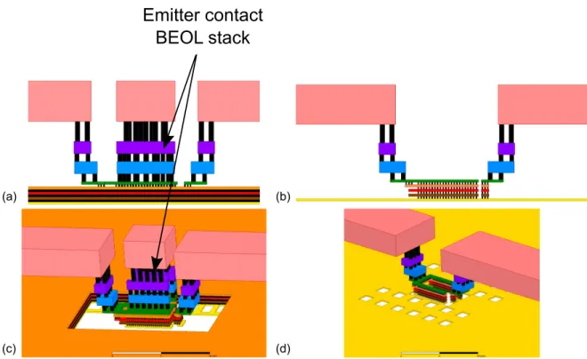
In this work, the 55 nm SiGe:C BiCMOS (BiCMOS055, or B55 for short) by STMicroelectronics will be studied [16,17]. ST’s BiCMOS combines a CMOS and a npn SiGe HBT, the architecture of which has been developed through generations from the early single-polysilicon quasi self-aligned architectures to modern double-poly fully self-aligned (DPSA) – whose technology is used for the B55 too. Owing to their digital density 5 times higher than previous 130 nm technology, B55 well serves optical, wireless and high-performance analogue applications.
B55 is based on a 55 nm triple gate CMOS platform (55 nm being the average distance between identical features in an array of memory cells made with this technology), featuring both Low Power and General Purpose CMOS.
The SiGe HBT has to provide minimum access resistances to the emitter, base and collector, and minimum base-collector and base-emitter capacitances as well. It features the double-poly self-aligned architecture with selective epitaxial growth (DPSA-SEG) of the boron-doped SiGe:C base (C hinders boron diffusion) (Fig.1.8a).
The double-poly architecture provides access from the contact regions to the emitter and in-trinsic base regions by poly-Si layers which dielectrically isolate against the surrounding transistor regions: RE, RBx, CBE, CBCxare kept small.
While this practice is quite common, what differentiates the HBT fabrication is the growth of the base. The SEG compared to non-selective epitaxial growth is the most attractive process for its simplicity (since only one lithographic step is needed) and its effectiveness in the quality of self-alignment of the emitter with the base. It is inserted in the fabrication process between gate poly-Si deposition and gate patterning of CMOS to reduce the total amount of thermal energy transferred to the CMOS during elevated temperature operations. However, improvement compared to the current performance level are hardly possible with this approach, due to the impossibility to cut the extrinsic base resistance RBx[8].
ST’s SiGe HBT (Fig.1.10a) comes in three collector flavours, with different fT×BVCEOtrade-offs:
High Speed (HS), Medium Voltage (MV) and High Voltage (HV). The back-end (made of 8 copper layers and an aluminium cap, Fig.1.10b) will be extensively considered in the following; it is fully compatible with CMOS and provides enhanced mmW performance [18].
fT and fmax performances are obtained thanks to the higher collector current densities and
reduced parasitic resistances and capacitances allowed by the vertical and lateral scaling of tran-sistors. In Fig.1.11, we can observe such an improvement from older technologies notably at
(a) TEM cross-section of a 0.1 × 4.9µm2HS SiGe HBT (zoom in on emitter and base regions)
(b) SEM cross-section showing main devices and back-end up to metal 8
Figure 1.10: BiCMOS055 by STMicroelectronics (after [16]).
Figure 1.11: Evolution of fTand fmaxvs. collector current density in STMicroelectronics SiGe BiCMOS
tech-nologies (after [17]).
relatively high collector current density, with HF performance standing out for B55. Then the per-formance is degraded by heavy injection effects. By increasing fTand fmax, the collector-emitter
breakdown voltage consequent reduction points out the need for a trade-off. However, the fT×
BVCEOof B55 is the highest of all ST’s BiCMOS.
Whereas early 90 nm BiCMOS technologies featured HBTs with HF performance that reached (fT, fmax) = (130,100)GHz [57], measured results for the SiGe HS HBT in B55 prove a better HF
behaviour, the couple of values being (fT, fmax) = (326,376)GHz.
Advancements on the BiCMOSB55 process led STMicroelectronics to develop the next bipolar CMOS technology: BiCMOS55X. The optimization of the vertical profile including the thermal budget and the fully implanted collector development showed a very good potential (450 GHz fT
was demonstrated in [42]). The new emitter/base architecture called EXBIC [122] is certainly the most challenging part of these developments. Such an architecture aims at the realization of the targeted 600 GHz fmaxperformance.
Measurement and Calibration Basics
Contents2.1 Vector Network Analyser. . . 17
2.1.1 Signals and Scattering Parameters . . . 17
2.1.2 Architecture of the VNA . . . 19
2.1.3 Measurement Errors and Calibration Techniques . . . 21
2.2 On-Wafer Measurements at High Frequency . . . 26
2.2.1 Radio-Frequency Probes. . . 26
2.2.2 Calibration on a Dedicated Substrate . . . 27
2.2.3 De-Embedding Routines . . . 29
2.2.4 Characterization at Millimeter Wave Frequencies . . . 31
T
HE PROGRESSof electronics over the course of the years has made possible to build complex circuits made of devices operating at very high frequencies, and this trend is expected to con-tinue. The growing complexity of high frequency integrated circuits relies on the quantification of several nano-electronic device properties that need to be precisely modelled and characterized.Indeed, it is fundamental to ensure that a device for any millimeter-wave application behaves as expected in order to provide circuit design engineers advanced and accurate libraries (design kits) for CAD platforms. The libraries implement lumped electrical circuit-based models, whose parameters have to be extracted from trustworthy millimeter wave frequency measurements and verified and elaborated by simulations, either of passive or active devices (in this case, through compact models, depicting the underlying physics, based on semiconductor, electromagnetical and thermal equations). For instance, if a designer employ a transistor to work at a certain fre-quency in his/her system, he or she expects a certain output power from the model, which there-fore needs to rely on precisely characterized and well-calibrated measurements. Therethere-fore, much of the semiconductor HF characterization deals with the mathematical removal of test fixtures and on-wafer parasitic elements.
In this chapter, we will describe how small-signal measurements are performed and learn that, in fact, the raw measurement data themselves do not describe at all the intrinsic device behavior, and need for additional data processing steps.
The most wide-spread measurement system, the vector network analyser, will be described and the signal quantities will be rigorously defined, before plunging into an overview of the as-sembly parts of network analysers, with their functions and components accurately portrayed. The notion of measurement error terms will let us introduce some of the most common calibra-tion routines, which effectively provide a solucalibra-tion for correcting the errors. The challenges of going up in frequency and perform measurements, the dedicated setup and adjustments of calibrated data, and, finally, the used measurement configuration and instrumentation, will conclude the chapter.
2.1 Vector Network Analyser
2.1.1 Signals and Scattering ParametersVector network analysers (VNAs) are measurement systems which are used to analyse circuits from small components (transistors, filters, amplifiers, etc. . . ) to more complex modules by comparing the real and imaginary part of an incident signal (the one generated by the VNA) with the trans-mitted signal (the one passing through the system and measured on another side) or the reflected signal (the one reflected by the input of the system).
Those RF signals are defined by convention as “a” for the incident wave and “b” for the re-flected (or transmitted) wave. “a” and “b” are the so-called "power waves" and their squared ab-solute values (i.e. “|a|2” and “|b|2”) represent the true incident and reflected powers, respectively. In a general way, they are defined as:
a = V + Z0I 2pRe(Z0) = V + p Re(Z0) (2.1) b = V − Z ∗ 0I 2pRe(Z0) = V − p Re(Z0) (2.2) where Z0is the characteristic impedance of the line and V+ and V−are the incident and
re-flected voltage wave amplitudes, respectively. We can thus observe that the power waves carry the same information as the voltages. For a lossless line (Z0positive and real), the reflection coefficient
at port i is: Γi,V − i V+ i =bi ai = Zi− Z0 Zi+ Z0 (2.3) where Ziis the impedance at port i .
VNAs can perform several measurements of these quantities and retrieve fundamental infor-mation about the system under test, such as the scattering parameters (S-parameters). These quantities describe the electrical behavior of a linear devices and are defined as ratios of the re-flected (or transmitted) waves to the incident ones. Some VNAs can be mounted with up to 48 ports [105]. In general, for a n-port network:
b1 .. . bn = s11 · · · s1n .. . . .. ... sn1 · · · snn · a1 .. . an (2.4)
where bi and aiare the incident/reflected waves, respectively, for each port i , which is termi-nated to a specific Z0i impedance. For a 2-port network (Fig.2.1), however, the previous formula
can be reduced to the following system:
b1= s11a1+ s12a2 b2= s21a1+ s22a2
(2.5) so it’s easy to define:
s11= b1 a1 ¯ ¯ ¯ ¯ a2=0 s21= b2 a1 ¯ ¯ ¯ ¯ a2=0 s12= b1 a2 ¯ ¯ ¯ ¯ a1=0 s22= b2 a2 ¯ ¯ ¯ ¯ a1=0 (2.6)
Scattering parameters are particularly suited for active devices under test (DUTs) such as tran-sistors, considering that, for defining other electrical parameters (such as Y, Z and H), it would be
a
a
b
b
1 2 2 1s
s
s
s
11 22 12 21Figure 2.1: A 2-port network where signals and S-parameters are shown.
necessary to effectively create short and open circuits for measuring them, which is extrimely hard and imprecise, particularly at high frequencies (tuning stubs would be needed) [11].
Flow charts are useful schematic descriptions of networks where signals and parameters are presented in blocks so that the relation between them can be easily explicated by following the block-to-block connections. As way of example, Fig.2.2shows an equivalent flow chart indicat-ing all coefficients appearindicat-ing in a 2-port network when a real voltage source is applied at port 1 (voltage Vg, impedance Zg6= Z0) and a generic load at port 2 (ZL6= Z0).
s
11
s
21
s
22
s
12
𝛤
S
𝛤
L
a
a
b
b
1
2
2
1
Figure 2.2: Flow chart representing all reflection and transmission coefficients for a 2-port network when applying a voltage generator at port 1 at a given load at port 2.
In this case, a1can be written as: a1= V1+ Z0I1 2pZ0 = Vg p Z0 Zg+ Z0 (2.7) where the second equation comes from a simple voltage divider at the entrance of the DUT, V1= Vg
Z0
Zg+ Z0
, supposing that the impedance of the network is the characteristic impedance. From the previous diagram, the input reflection coefficient for a generic load is:
s110 =b1 a1 ¯ ¯ ¯ ¯ ΓL6=0 =a1s11+ a1c a1 (2.8) where c takes into account every contribution from the input of the DUT on, and can is calcu-lated as: c = ΓL µ c s12 s22+ a1s21 ¶ s12 (2.9)
s011= s11+
s21s12ΓL
1 − s22ΓL
(2.10) This equation shows that, when excitated by an external stimulus, the reflected wave at the entrance of the stimulated system depends on all the scattering parameters of the network, as well as, by the reflection of the signal, on the load. It is only when the load is perfectly matched to the characteristic impedance of the network (ZL= Z0, or, equivalently,ΓL= 0), that s11equals the
reflection coefficient at port 1, s011. Also, one can realize that by measuring four well-known loads, all the S-parameters of the network can be found.
2.1.2 Architecture of the VNA
S-parameters are complex numbers and in microwave devices, they can be employed to calculate some important qualities, or figures of merit, such as gain, losses, reflection and amplification, over a certain range of frequency. Vector network analysers are able to evaluate both magnitude and phase of the S-parameters of a DUT (single or multi-port), by sweeping up to THz frequencies (with the use of dedicated extenders, as it will be discussed later) and by controlling the injected power at each port. A scalar network analyser (SNA), which compared to VNA can only measure magnitudes of signals, is less pricey and can be used for similar purposes. However, some of the benefits of a VNA over a SNA are [47]:
• full system error correction (for systematic errors);
• complex parameters can be translated to the time domain; • de-embedding/embedding capabilities;
• Smith chart drawing.
In this manuscript, only VNAs are used as measuring tools.
In Fig.2.3, a simplistic block diagram of the main components of a VNA is shown [47]. It can be grouped into four blocks according to its functions [116]:
• a generator stage, to output a stimulus in two different modes, as power and frequency sweep;
• a signal separation stage (or test set), which separates the forward and reverse waves. A power
splitter and a directional element are part of it: the former provides the same values for a1
and a10, that are proportional to the generated signal (a100= αa01= αa1,α being an arbitrary
proportionality constant), while the latter (a coupler, at high frequency), is in charge of sep-arating the wave directed to the DUT from the one reflected;
• the test ports, which is the physical interface between the VNA and the DUT; • a receiver and analyser module.
Z
Z
Z
Z
Z
0 0 0 0 0 directional element reference receiver measurement receiver generator power splitter (1) (2) (3) s s s b b b a a a a' a'' DUT DUT 2 2 32 21 31 3 1 1 1 DUTSignal Generator The first stage deals with the signal generation. Engineers have many degrees
of freedom for the choice of the shape of signal in modern VNAs; which can be sinusoidal, as well as pulsed, squared, modulated, etc... For this purpose, a voltage-controlled oscillator (VCO) such as a crystal oscillator plus a feedback, provided by a phase locked loop (PLL), generate a signal sweeping in a desired frequency range. In addition to that, an automatic loop control (ALC) stage ensures to deliver a controllable power to the DUT and a proper level for the operation in the case of an active device.
Directional Element Next, both the generated and received signals have to be sampled in order
to compute the S-parameters. Ideally, the VNA behaves in such a way that the reflection coeffi-cient of the DUT is given by the ratio of the measured wave b3and the incident wave a1(Fig.2.3).
Indeed, the directional element adds its contribution to the measured value M = b3/a01, so that
M = RΓDUT, whereΓDUT = bDUT/aDUT= a2/b2. R is called reflection tracking, and is defined as
R = s21s32: it takes into account the attenuation due to the passage of the signal through the
di-rectional element. We are assuming here that a1 is constant and identical to the one used as a
reference, which is achieved by the use of the splitter. Yet, we are not considering some non-ideal effects which affect the measurement. First of all, s316= 0, which means that a certain quantity of
the input signal deviate from the path to the DUT and adds up to the measured power wave. We can thus write:
M = R µ s 31 s32s21+ ΓDUT ¶ = R¡D + ΓDUT¢ = R ΓDUT(x + 1) (2.11)
We introduce the quantity D, called directivity. x = D/ΓDUT is a relative deviation due to a
systematic error given by s31and requires correction. Also, multiple reflections at port 2 of the
coupler should be considered. If we stop at the second reflection, after which the reflected power is negligible, we get:
a2= b2ΓDUT¡1 + S ΓDUT¢ = b2ΓDUT(1 + y) (2.12)
where S is the reflection coefficient of the test port (s22), also called test-port match, and it
contributes as a relative error y = S ΓDUT. So by summing up all the results, the previous formulas
yield:
M = R£D + ΓDUT¡1 + S ΓDUT¢¤ (2.13)
The directivity and the test-port match limit the measurement accuracy by adding uncertainty to the measurement. If |ΓDUT| is small, the error given by D will limit the measurement, while if
|ΓDUT| is large, S will be the bound. R is independent of |ΓDUT|, whereas it is not the case for D and
S.
Test Ports The connection between the VNA and the device are the so-called "ports" and the
majority of VNAs comes with 2 or 4 of them. Often times, they are coaxial sockets located in the front side of the network analyser, allowing to employ coaxial cables. The use of coaxial cables rather than rectangular waveguides to carry the signals is made, of course, for simplicity of han-dling thanks to their flexibility, and also because of the strong advantage to produce a pure TEM wave, thus presenting no low frequency cutoff, and withstand a broad spectrum of frequency from DC to tenths of gigahertz. To connect and contact them to the device ports, additional elements are needed, such as tees and high frequency (also called radio frequency, RF) probes. Non-idealities in the signal separation stage and in the test ports, however, affect the quality of the measurement and some procedures grouped under the name of "calibration", which are at the core of this work, need to be performed to "clean off" the raw measurements.

![Figure 1.5: A spike appears in the emitter-base heterojunction when different materials are put into contact (after [123]).](https://thumb-eu.123doks.com/thumbv2/123doknet/14543240.725169/19.892.212.699.130.423/figure-spike-appears-emitter-heterojunction-different-materials-contact.webp)
![Figure 1.7: Different displacement of the conduction band in BJT and SiGe HBT (after [74]).](https://thumb-eu.123doks.com/thumbv2/123doknet/14543240.725169/23.892.260.654.109.356/figure-different-displacement-conduction-band-bjt-sige-hbt.webp)
![Figure 1.8: Schematic cross-section of high-speed SiGe HBT device architecture (after [90]).](https://thumb-eu.123doks.com/thumbv2/123doknet/14543240.725169/24.892.147.723.104.423/figure-schematic-cross-section-speed-sige-device-architecture.webp)