HAL Id: tel-00595302
https://tel.archives-ouvertes.fr/tel-00595302
Submitted on 24 May 2011HAL is a multi-disciplinary open access archive for the deposit and dissemination of sci-entific research documents, whether they are pub-lished or not. The documents may come from teaching and research institutions in France or abroad, or from public or private research centers.
L’archive ouverte pluridisciplinaire HAL, est destinée au dépôt et à la diffusion de documents scientifiques de niveau recherche, publiés ou non, émanant des établissements d’enseignement et de recherche français ou étrangers, des laboratoires publics ou privés.
Dingwei Zheng
To cite this version:
Dingwei Zheng. Study and manipulation of photoluminescent NV color center in diamond. Other [cond-mat.other]. École normale supérieure de Cachan - ENS Cachan; East China normal university (Shanghai), 2010. English. �NNT : 2010DENS0031�. �tel-00595302�
Study and Manipulation
of Photoluminescent NV Color Center
in Diamond
Étude et Manipulation des Propriétés de Spin du Centre Coloré
photoluminescent NV dans des nanocristaux de diamant
to obtain the title of
PhD of Physics
of École Normal Supérieure de Cachan
and East China Normal University
Defended by
Dingwei ZHENG
October 27, 2010
Jury :
Reviewers : Prof. Nicolas TREPS - LKB (Université Pierre et Marie Curie) Prof. Huan-Cheng CHANG - IAMS (Academica Sinica)
Examinators : Prof. Longsheng MA - LPS (East China Normal University) Prof. Jean-François ROCH - LPQM (ENS de Cachan)
Advisor : Prof. François TREUSSART - LPQM (ENS de Cachan)
Contents
1 Introduction 1
I Optical property of NV color centers 5
2 NV0 and NV− color centers in diamond 7
2.1 Overview of diamond and color centers in diamond . . . 7
2.1.1 General introduction of diamond and defects . . . 7
2.1.2 Fabrication of diamond crystal . . . 8
2.2 NV color centers in diamond. . . 10
2.2.1 Creating NV color centers in diamond . . . 10
2.2.2 Optical addressing of single NV color center . . . 12
2.2.3 Photoluminescence of NV0 and NV− color centers . . . 12
2.3 Study of photochromic effect between NV0 and NV− color centers . . . 15
2.3.1 Review of the charge state study of NV color centers . . . 15
2.3.2 Photochromic effect of NV color center in bulk diamonds . . . . 16
2.3.3 Photochromic effect of a single NV color center in nanodiamonds 19 2.4 Conclusions . . . 22
3 Control of the NV photoluminescence 23 3.1 Introduction . . . 23
3.2 Experimental setup and sample preparation . . . 24
3.2.2 Confocal microscopy setup . . . 25 3.2.3 Sample preparation . . . 26 3.3 IR effect on the luminescence of NV color center . . . 27
3.3.1 Effect of IR excitation on the luminescence of NV color centers in nanodiamonds . . . 27 3.3.2 Response time of the IR pulsed excitation . . . 29 3.3.3 Time delay dependence of infrared excitation quenching effect . . 30 3.3.4 Power dependence . . . 34 3.4 Infrared excitation effect on PL of NV color centers in a bulk diamond . 35 3.5 Model of photoluminescence quenching effect due to IR pulsed excitation 38 3.6 Conclusions . . . 39
4 Super-resolution optical imaging of NV color centers in
nanodia-monds 41
4.1 Microscopes allowing nano-imaging . . . 41 4.1.1 Introduction. . . 41 4.1.2 Resolution limit of far field optical microscopy. . . 42 4.2 Resolution improvement with an annular shaped illumination beam . . . 45 4.3 Super-resolution imaging with a focused doughnut spot. . . 47 4.4 Super-resolution imaging based on IR pulsed excitation quenching effect 50 4.5 Conclusions . . . 51
II Spin property of NV color centers 55
5 Introduction of ODESR experiment 57
Contents 3
5.2 Energy calculation of NV− color center in the ground state . . . 58
5.2.1 NV spin Hamiltonian. . . 58
5.3 Working principle of ODESR experiment. . . 59
5.3.1 ODESR experimental setup . . . 63
5.3.2 Sample discription . . . 63
5.3.3 Excitation lasers . . . 63
5.3.4 Microwave generation and detection . . . 63
5.4 Conclusion. . . 67
6 Manipulation of NV color centers 69 6.1 Introduction . . . 69
6.2 The modulation study of ODESR spectrum . . . 69
6.3 NV spin manipulation . . . 72
6.3.1 NV spin manipulation with a continuous microwave field . . . 72
6.3.2 NV spin manipulation with a static magnetic field . . . 73
6.3.3 NV spin manipulation with a pulsed microwave field . . . 75
6.4 Conclusions . . . 78
7 The ensemble of NV spins in diamond single crystal 81 7.1 Introduction . . . 81
7.2 ODESR of an ensemble of NV color center in bulk diamond . . . 82
7.2.1 ESR measurement . . . 82
7.3 Lifetime measurement . . . 83
7.4 Conclusions . . . 87
8.1 Introduction . . . 89
8.2 Experimental setup . . . 90
8.3 Transition dipoles and spin axis of a single NV center. . . 90
8.3.1 Analysis of excitation polarization dependence . . . 92
8.3.2 Determination of individual dipole orientation . . . 95
8.4 Determination of the orientation of a single NV electron spin . . . 98
8.5 Conclusions . . . 100
9 Conclusion and outlook 103
Chapter 1
Introduction
At present, quantum information is a rapidly developing branch in modern science. The unit of quantum information is the quantum bit (qubit) which is a two-level quantum system. Unlike classical digital states, a two-state quantum system can actually be in a superposition of the two states at any given time. Quantum information differs from classical information in several respects:
• Reading of a qubit results in a projection on a basis. • An arbitrary state cannot be cloned.
• The state may be in a superposition of basis values.
Solid-state systems, in which spins (electron and nuclear) of various defects and impu-rities in semiconductors are used as stationary qubits. Quantum dots [119] and single molecules [85] have been utilized to generate single photon emission. But perhaps the most promising and applicable source of single photons for practical applications arises from optical defects in diamond. It is the only material presently known which con-tains room temperature photostable defects capable of producing single photon pulses with a high effciency. To date, of the over 500 known defect centers in diamond, only four have been identified as single photon emitters: silicon vacancy (SiV) center [139], Nikel related complex [49,144], NV color center [75], and Chromium related complex [3]. The very low emission rates of the SiV center and the difficult to controllably fabricate Ni and Cr related centers at the single level, limit the practical applications with these centers. In the contrary, the nitrogen-vacancy (NV) center is up to now the best candidate for quantum information applications, owing to its room-temperature photostability, allowing single photon generation, and to its capability of electron spin manipulation.
About ten years ago it was noted that the NV in its singly-charged state, NV− has many of the desired attributes of a qubits [86]: its triplet ground state provides long coherence spin states to manipulate the qubit, and it has a convenient optical transition in the visible. In recent years much progress has been made towards the realization of quantum information processing (QIP) based upon NV centers in diamond. We
can build an efficient single-photon source [17,75]; Optical and microwave qubit gate operations have been performed [26] using optical readout of single electron [70] and nuclear spins [71, 29, 143]. Electron spin coherence times exceeding 1 ms at room temperature [10] have been observed with nuclear spin-zero environment of the diamond lattice. A variety of techniques has been employed for coupling NV centers in diamond to optical microcavities [11, 12,109,126] and waveguides [46] for realization of large-scale quantum information processing and for quantum repeater systems.
Optical readout of the NV− electron spin resonance has also allowed advanced application to nanomagnetometry. Hgh sensitivity magnetometers have been devel-oped with different techniques such as: superconducting quantum interference device (SQUID)[15], scanning Hall probe microscopy [24], magnetic force microscopy (MFM) [94], and magnetic resonance force microscopy (MRFM) [118,88]. Though these tech-niques offer high sensitivity, they require cryogenic cooling or vacuum conditions, they are feasible to some particular domain. In contrast, the NV color center has several outstanding advantages for this application. Optical polarization and spin state read-out facilitates convenient and nonivasive far field detection. The atomic NV sensor permits the minimization of the sample-sensor distance, and the manipulation can be carried out at room temperature [9]. By using NV centers, researchers are able to image the vector magnetic field [87, 129], to sense the fluctuating nanoscale magnetic fields [58,95] and also to readout single nuclear spins [71,128,106]. Recently, using a mag-netic tip to produce a large field gradient, NV diamond has achieved 5 nm resolution under ambient condition [10].
Numerous studies have been done to understand the NV− center electronic states and energy levels. Uniaxial stress measurements [33] have determined that the NV center has C3v symmetry, with the ZPL emission band associated with an A to E dipole transition. The hole burning EPR signal [112], optically detected magnetic res-onance(ODMR) [107], electron spin resonance [113,84] and Raman heterodyne experi-ments [89] have established the energy level scheme of NV−center . Several theoretical works have been done, using the Linear Combination of Atomic Orbitals (LCAO) ap-proach to build the electronic orbitals to describe the possible quantum states, looking at the NV center as a molecule [81]. Moreover, group theory results are used to take into account the symmetry of the diamond crystal, and of the NV itself [91,92]. How-ever, the knowledges about NV color center level structure are still incomplete and numerous studies are in progress to unveil unknown properties.
In this dissertation, we investigate a variety of aspects of NV centers in the dia-mond including: production, photoluminescence property, electron spin property etc. by means of confocal microscopy and optically detected magnetic resonance (ODESR) technique. Besides, different means to achieve far field optical super resolution will be discussed as well. The thesis contains two parts, Part I from Chapter 2 to Chapter 4,
3
which mainly concern the optical properties of NV color center. Part II includes Chap-ter 5 to ChapChap-ter 8 and deals with the spin manipulation and spin readout technique of NV color center. The thesis is organized as follows:
In Chapter 2, we will firstly review different techniques for producing diamond and creating NV color centers. Then the photochromic effect of NV centers due to the modification of NV center charge [NV− ↔NV0] is investigated. The photochromic effect of a single NV color center is of great interests in order to better control the NV center charge state NV0 and NV− centers. Recently the negatively charged form NV− has the remarkable spin properties optically detectable.
In Chapter 3, we study the reversible quenching of NV color center photolumines-cence under infrared (IR) pulsed laser irradiation in diamond. Several approaches are used to interpret this effect. We conclude that the IR effect is induced by multi-photon absorption of diamond crystal. It is possible to use this effect for STED-like super resolution imaging of NV center in diamond nanocrystals.
In Chapter 4, various far field optical super-resolution techniques are demonstrated. This include annular shaped illumination beam, or doughnut shaped beam in the regime of saturation, and IR pulsed excitation quenching effect. Their working principles and spatial resolution improvement are discussed.
In Chapter 5, the electron spin property of NV color center is reviewed briefly. Optically detected electron spin resonance (ODESR) experiment is applied to the NV− color center. The samples and experimental setup used in the second part is also introduced.
In Chapter 6, the NV center electron spin is manipulated with a static magnetic field, continuous microwave field and pulsed microwave field. Properties of NV color centers (PL lifetime, PL intensity, Rabi-oscillation, coherence time) are investigated through these manipulations.
In Chapter 7, the ODESR experiment is applied to an ensemble of NV colors. The four possible orientations of NV spin axis are figured out from the Zeeman shift of NV electron spins. We also developed a fluorescence lifetime monitoring method to have access to the magnetic field without the necessary of microwave excitation of the ESR. Moreover, it is possible to evaluate the uniformity of spin orientation distribution of an ensemble of NV centers from this experiment. This is of great importance for the application of ensemble of NV centers as a magnetic field sensor.
In Chapter 8, the NV spin and NV optical dipoles’ orientations in the space is de-termined using the Zeeman effect and polarization measurements. These two different approaches lead to an identical result. This is a vital study for efficient coupling of
Part I
Optical property of NV color
centers
Chapter 2
NV
0
and NV
−
color centers in
diamond
Contents
2.1 Overview of diamond and color centers in diamond . . . 7
2.1.1 General introduction of diamond and defects . . . 7
2.1.2 Fabrication of diamond crystal . . . 8
2.2 NV color centers in diamond . . . 10
2.2.1 Creating NV color centers in diamond . . . 10
2.2.2 Optical addressing of single NV color center . . . 12
2.2.3 Photoluminescence of NV0and NV− color centers . . . . 12
2.3 Study of photochromic effect between NV0 and NV− color centers . . . 15
2.3.1 Review of the charge state study of NV color centers . . . 15
2.3.2 Photochromic effect of NV color center in bulk diamonds . . . . 16
2.3.3 Photochromic effect of a single NV color center in nanodiamonds 19 2.4 Conclusions . . . 22
2.1
Overview of diamond and color centers in diamond
2.1.1 General introduction of diamond and defects
As a precious gemstone, diamonds are fancy-colored, in addition to its superlative physical qualities, the highest hardness and thermal conductivity of any bulk material, the study of diamond covers numerous domains such as gemology, material, biology, physics, etc.
Diamond is an allotrope of carbon, where the carbon atoms are arranged in a variation of the face-centered cubic crystal structure, called a diamond lattice. Such
special structure results in the strong covalent bonding between its atoms, which is the origin of its hardness. Diamond has a wide band gap of 5.5 eV corresponding to the deep ultraviolet wavelength of 225 nm. This means pure diamond should transmit visible light and appear as a clear colorless crystal. As the materials scientist F. Franck said, “Crystals are like people, it is only the defects that make them interesting. ” In fact, colors of diamonds come from small amounts of defects or impurities (about one per million of lattice atoms) in diamond lattice. The luminescent defects, which have special energy structures, are able to absorb or fluorescent photons with special wavelengths. Thanks to different kinds of defects, the diamonds are rendered blue (boron), yellow (nitrogen), brown (lattice defects), green (nickel), purple, pink, orange or red as seen in Figure2.1, which not only make it beautiful but are also interesting for scientific researches. Such kind of luminescent defects are called color centers and more than 500 color centers in diamond have been catalogued until now [145].
Figure 2.1: Colorful diamonds with luminescent defects in diamond lattice.
2.1.2 Fabrication of diamond crystal
Most natural diamonds are formed at high-pressure high-temperature conditions exist-ing at depths of 140 to 190 kilometers in the Earth mantle [20,45], the growth occurs over periods from 1 billion to 3.3 billion years. Diamonds can also be obtained by syn-thetic method, which can satisfy the large demand fro the gemological and industrial use. The High-Pressure High-Temperature (HPHT) procedure is the first developed synthesis of diamond [22]. It became a commercial reality during the 1950s and remains the major manufacturing method for synthetic diamond products. In essence, HPHT emulates the way in which natural diamonds are created deep in the earth where the
2.1. Overview of diamond and color centers in diamond 9
enormous pressure makes carbon crystals with the denser structure of diamond more stable than those of other carbon allotropes such as graphite (Figure2.2). The HPHT growth process offers a significant degree of control over the quality and geometry of diamond obtained. Most diamond produced by this method is small grains of type Ib. However, longer controlled growth periods enable production of single crystal Ib stones with dimensions routinely up to 8 mm. The drawback of this technique is that the experimental condition of pressure as high as 60 000 atmospheres is quite tricky and costly.
Figure 2.2: Phase diagram for carbon indicating main regions of pressure-temperature space in which diamond growth occurs [8].
Another popular method of growing synthetic diamond is Chemical Vapor Depo-sition (CVD). At low pressure (below atmospheric pressure), a mixture of carbon-rich gases (typically 1 to 99 methane to hydrogen) is broken into fragments and reassemble into diamond film on a surface by microwaves, hot filament, arc discharge, welding torch or laser. The growth rate is typically about 1 µm per hour. Techniques such as increasing the pressure of the carbon-rich gas [135] have been developed to accelerate the growing processor. The CVD diamonds are thin and flawed films. The flaws can be reduced by choosing a pure diamond as the substrate.
Diamond nanocrystals can also be formed by detonating certain carbon-containing explosives in a metal chamber. These diamond nanocrystals are called “detonation nanodiamond ”. The explosion heats and compresses the graphite to an extent sufficient for its conversion into diamond. The product is always rich in graphite and other non-diamond carbon forms and requires prolonged boiling in hot nitric acid (about 1 day at 250 ◦C) to dissolve them.
2.2
NV color centers in diamond
2.2.1 Creating NV color centers in diamond
The NV color center in diamond lattice is one of the most well known color centers. It is a point defect in the diamond lattice, formed by a substitutional Nitrogen atom combined with an adjacent vacancy in diamond lattice as shown in Figure2.3. It can be viewed as a molecule trapped in diamond lattice. The NV color center absorbs well the photons in VIS-UV range and fluorescent broadly in the VIS range as shown in Figure ??. Bright, photostable luminescence, working at ambient condition characters of NV colors enables it for the applications of scientific imaging, biolabeling as well as quantum communication and computing.
Figure 2.3: Schematic representation of the NV center structure.
NV color center can be found in natural diamonds, but the concentrations and locations of defects are quite different from one to another. In order to controllably create NV, some synthesize techniques have been developed. The NV color centers can be created after obtaining diamond crystal or during diamond growth process. Figure 2.4 shows a common technique of producing NV color center, which begins from the substitutional nitrogen atoms (called C or P1 centers in diamond literature). Diamonds containing such impurity are firstly irradiated by high-energy particles such as electrons, protons, neutrons, ions and gamma particles, which produce lattice vacancies. Then the sample is annealed at temperatures around 800◦C, in order to mobile the vacancies. At this temperature, substitutional nitrogen produces strain in the diamond lattice and efficiently captures moving vacancies, then forms the NV color center. It was recently demonstrated that some oxidate procedure such as acid cleaning or thermal oxidation were used to remove the surface contamination caused by annealing, and therefore increase the brightness of nanodiamonds.
2.2. NV color centers in diamond 11
50μm
Raw diamond Irradiated (electron beam)
Annealed (800°C, 2 hours)
Figure 2.4: The common process of creating NV color centers. Images are obtained by measuring photoluminescence of the diamond.
Another approach of creating NV color centers is nitrogen implantation in a very pure type IIa diamond [96]. In this approach, nitrogen atoms are implanted by fo-cusing a nitrogen ion beam on the diamond surface, meanwhile, vacancies are created during the slowing down of the implants. The NV center can be formed upon anneal-ing. The advantage of this technique is the low paramagnetic impurity contaminant, namely paramagnetic nitrogen. It is well known that for quantum information science, spin qubits have to be introduced in a spin-free lattice to ensure long coherence time, paramagnetic nitrogen substitution forms a spin bath thus limiting the coherence time [132]. The efficiency of this process is limited by the number of vacancies available in the vicinity of the N stopping position and by the capture cross section of vacancies by nitrogen. Recently, a two step implantation process which includes low dose N+2 molec-ular ion implantations followed by high dose C implantation has been demonstrated to increase the generation efficiency of NV centers by over 50 % [102].
The CVD-grown diamond is unique in that NV centers can be created during the synthesis process. The NV color center incorporated diamond film can be grown with 0-0.1% N2, 0.7% CH4, 99.2% H2 gas mixture, at about 800◦C substrate temperature and low pressure [111]. The NV center concentration varies with the nitrogen doping levels. Single defects can be created by optimizing the nitrogen doping levels.
In the frame work of this dissertation, we have used samples fabricated by different fabrication methods, such as HPHT and CVD. The NV centers are created by high dosage irradiation with electron, proton and nitrogen particles.
2.2.2 Optical addressing of single NV color center
Optical excitation and detection of the NV color centers photoluminescence(PL) is realized with a home-built setup, illustrated in Figure 2.5. The confocal microscopy (left part) allows to address single NV emitter and provide very high SNR (signal to noise ratio) photoluminescence. The NV color center is excited by either a cw laser or a pulsed laser (wavelength=532 nm) depending on the application. The excitation beam is focused onto the sample using a high numerical aperture microscope objec-tive (NA=0.95) working in air. The focusing point is raster scanned relaobjec-tive to the sample with nanometric resolution, using a piezoelectric driven mirror tilting system. The photoluminescence of the excited NV center is collected by the same objective and spectrally filtered from the remaining pumping light by a long-pass filter with a wavelength cut-off at 580 nm, and a transmission >80% in the range 580-750 nm. A standard confocal detection system is also used to select the luminescence coming from a sample volume of about 1.43 µm3. The mirror M2 is mounted on a flip-flop base, which enables us to measure either the spectrum or intensity of the photoluminescence. In order to identify the single photon emission, we use the so-called Hanbury-Brown-Twiss (HBT) technique as shown in the right bottom side of Figure 2.5. The PL beam is divided into two identical beams using a 50/50 beam splitter, and detected by two avalanche photodiodes (APD), the signals from two APDs are analyzed with the correlation function.
g2(τ ) = < n1(t)n2(t + τ ) > < n1(t) >< n2(t + τ ) >
, (2.1)
where n1(t) [n2(t+τ )] is the number of counts registered on the detector APD1 (APD2) at time t [t + τ ]. The < · · · > symbol means the time average computed by integrating over a long time period. It turns out that g2(τ ) represents the coincident between counting of APD1 at the moment of t and APD2 at t + τ .
For a single photon beam, the photons come out with regular gaps between them. A single photon cannot be splitted by the beam splitter, and consequently it will be detected either by APD1 or APD2. Therefor, the coincidence detection between APD1 and APD2 at zero-delay (τ = 0) will be 0. This zero value of g(2)(0) obtained at zero delay time is then the signature of the single photon for all our work.
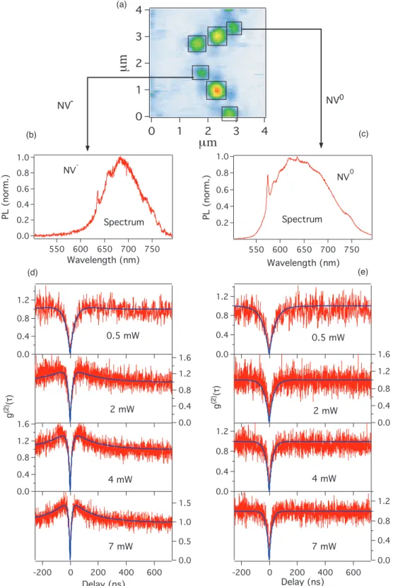
2.2.3 Photoluminescence of NV0 and NV− color centers
We first begin to study NV color center in diamond nanocrystals, the sample prepara-tion will be introduced in secprepara-tion 2.1. Figure2.6a is the scanning image of the sample with the confocal setup in Figure2.5. The bright spots are fluorescent emitters corre-sponding to NV color centers. It is well known that The NV color center exhibits two charge states: neutrally charged NV0, with a zero-phonon line at 575 nm (2.156 eV)
2.2. NV color centers in diamond 13 M1 DM Excitation laser F L1 PH L2 Coincidence M2 Spectrometer BS APD2 APD1 Delay HBT Confocal microscope M3
Figure 2.5: Optical setup used for detection of PL of NV color center in diamond: M1 is a mirror mounted on a piezoelectric driven tilting system; DM is a dichroic mirror which separates the fluorescence from the excitation light; M2 is a flip-flop mirror for choosing measurement of photon counting (on the avalanche photodiodes APD) or photoluminescence spectrum (using an imaging spectrograph SPC).
[98] and negatively charged NV−, with a zero-phonon line at 637 nm (1.945 eV) [33]. The charge state of NV centers can be determined from their spectrums (Figure 2.6b, 2.6c). Both NV− and NV0 centers can be found in this sample, the ratio is about 1:1. The g(2)curves of NV−and NV0 centers are depicted in Figure2.6. Figure2.6d and 2.6e are the g(2) curve of single NV− and NV0 centers at different excitation power. It is well known that NV− color center has a long lifetime metastable level (Figure 5.2a). When excited with a strong laser power and become saturated, the electron will be populated to the metastable level and results in the bunching effect [16] as shown in Figure 2.6d. In contrast, all the observations on single NV0 color centers showed no bunching effect for any excitation powers (see Figure 2.6e), which may leads to a conclusion that the NV0 color center is a two level system without the metastable state as shown in Figure 5.2b.
Our proposed energy level scheme of NV0 center lacks the dark metastable state compared to the NV− center. It is well known that the long-lifetime metastable state can trap the electrons and decrease the PL intensity of NV centers. The two-level NV0 center is hence supposed to have higher PL intensity compared to the NV− center. However, the fluorescence property of NV colors are strongly influenced by its ambient
g (2 )( τ) g (2) ( τ) (b) (d) (c) (e) 4 3 2 1 0
µm
4 3 2 1 0 µm (a) 1.2 0.8 0.4 0.0 1.6 1.2 0.8 0.4 0.0 1.6 1.2 0.8 0.4 0.0 1.5 1.0 0.5 0.0 600 400 200 0 -200 Delay (ns) 0.5 mW 2 mW 4 mW 7 mW 1.2 0.8 0.4 0.0 1.6 1.2 0.8 0.4 0.0 1.2 0.8 0.4 0.0 600 400 200 0 -200 Delay (ns) 1.2 0.8 0.4 0.0 0.5 mW 2 mW 4 mW 7 mW NV- NV 0 1.0 0.8 0.6 0.4 0.2 0.0 PL (norm.) 750 700 650 600 550 Wavelength (nm) NV -Spectrum 1.0 0.8 0.6 0.4 0.2 PL (norm.) 750 700 650 600 550 Wavelength (nm) NV0 SpectrumFigure 2.6: (a) is the scanning image of diamond nanocrystals containing NV color centers. (b) and (c) are the PL spectrum of a single NV− and a single NV0 color centers, (d) and (e) are the corresponding autocorrelation function measurements. All measurements are realized under the same experimental conditions and at room temperature.
2.3. Study of photochromic effect between NV0 and NV− color centers 15
A
E1
E2
A
E
NV
-
NV
0(a)
(b)
Figure 2.7: Proposal of energy diagram of NV− and NV0color centers. The 2-level structure of NV0center allows obtaining a perfect antibunching curve, while the 3-level structure of NV− color center causes the bunching effect.
conditions and its dipole orientations, it seems difficult to do the comparison in the the aspect of PL intensity. Fortunately, the photochromic effect of NV color center are able to switch the NV color center between different charge states, which is quite useful for investigating the single NV− and NV0 in the same site i.e. under the same condition.
2.3
Study of photochromic effect between NV
0and NV
−color centers
2.3.1 Review of the charge state study of NV color centers
When the NV center is present in a diamond crystal, a single charge state often domi-nates but both charge states can co-exist [80]. The charge state of NV color center was firstly supposed to depend on the nitrogen impurity according to studies on vacancy related impurities in diamond [34]. In order to explain the two state coexistence of NV0 and NV−, the impurities in the vicinity of the NV center was brought forward to dominate the charge state of NV center [30]. The study of vertical distribution of NV centers in high purity diamond indicated that the NV0/NV− intensity ratio increases during the first 150 nm of etching [121], which suggests that the charge state of NV center is dominated by an electronic acceptor layer near the surface.
These two charge states could be created independently but also can be transformed from one to the other by applying different kinds of excitations. This transformation is called photochromic effect since it changes the band gaps between two charge states. The photochromic effect, i.e. photon-induced transformation of charge state of NV color center has been discussed in various studies. Y. Dumeige et al [39] reported that by exciting a nanodiamond with a 500 nm femtosecond laser, a single NV− color center was first transformed to a single NV− color center combined with a single NV0 color center and finally become a single stable NV0 color center. N. B. Manson et al [90] reported a photochromic effect of an ensemble of NV color centers, and verified the proportion of the NV−and NV0color centers as a function of the excitation wavelength and excitation time. T. Gaebel et al [49] reported a reversible photochromism effect, by exciting NV color centers embedded in a bulk diamond with a continuous laser at λ = 514 nm, a single NV0 color center was ionized to a single NV− color center and finally relaxation to a single NV0 color center under dark condition. All these observations were generally attributed to electron excitation and capture dynamics between nearby nitrogen donors and NV centers.
Recently, selective oxidation have been applied on diamonds containing NV color centers which were created by ion implantation and annealing [47]. The oxidation converts neutral NV centers to negatively charged NV centers. The results suggest that the graphitic damage is one possible reason for the electronic depletion effect.
The photochromic effect has also been observed in our studied. The behavior differs from sample to sample, moreover, the observation of photochromic effect of a single NV color center enables us to investigate the photoluminescence of NV0and NV−color centers and their comparisons.
2.3.2 Photochromic effect of NV color center in bulk diamonds
The photochromic effect can be observed on both CVD and HPHT bulk diamonds. The CVD bulk diamond sample is provided by CEA-LIST (Laboratoire d’Intl´egration des Syst`emes et des Technologies, CEA Saclay). Nitrogens are implanted in diamond crystal by high energy irradiation, and then the sample is annealed with Oxygen gas at 450◦C for 8 hours. NV color center concentration is experimentally determined to be about 2×10³/µm3. We have studied the photochromism of this sample and the results are shown in Figure 2.8. Firstly, the sample is excited with low laser power (3 µW), the PL spectra shows that most of the centers are NV0. The spectra red shifts as we increase the excitation power, the ZPL of NV− center becomes more and more pronounced indicating the transition of NV0 centers to NV− centers. This photochromic effect is reversible. Indeed, as soon as we decreased the excitation power to 5 µW, the centers return to the former NV0 form.
2.3. Study of photochromic effect between NV0 and NV− color centers 17 NV0 NV -1.0 0.8 0.6 0.4 0.2 0.0 PL (Norm.) 750 700 650 600 550 Wavelength (nm) P_exc: 4 µW 1.0 0.8 0.6 0.4 0.2 0.0 PL (Norm.) 750 700 650 600 550 Wavelength (nm) P_exc: 20 µW 1.0 0.8 0.6 0.4 0.2 0.0 PL (Norm.) 750 700 650 600 550 Wavelength (nm) P_exc: 500 µW 1.0 0.8 0.6 0.4 0.2 0.0 PL (Norm.) 750 700 650 600 550 Wavelength (nm) P_exc: 5 µW NV0 NV0 NV0 NV -(a) (b) (c) (d)
Figure 2.8: Reversible photochromic of NV color centers in a CVD bulk diamond as a function of the excitation power. P_exc, the PL spectra red shifts when increase the excitation power, and recovers as soon as the excitation power decreases. The sample contains multiple NV color centers and it is excited by a continuous laser at λ=532 nm.
A type Ib HPHT bulk diamond provided by CEMHIT (Conditions Extrˆeemes et Mat´eriaux: Haute Temp´erature et Irradiation) Orl´ean also present the photochromic effect. This HPHT bulk diamond with intrinsic substitutional Nitrogens is irradiated by a proton beam then annealed at 800◦C for 10 hours. NV color centers are formed with high concentration which is experimentally measured to be about 7×10⁵/µm3. The PL spectras obtained by different excitation powers are shown in Figure 2.9. At low excitation power, the NV0 and NV− center co-exist identified by the ZPLs at 580 nm and 637 nm respectively. While at high excitation power, the NV0 ratio decreases, and even disappears at 12 µW. The excitation power is chosen in a random order, hence the photochromic effect of this sample is also reversible.
NV0 NV -1.0 0.8 0.6 0.4 0.2 0.0 PL (Norm.) 900 800 700 600 500 Wavelength (nm) P_exc: 25 nW (a) 1.0 0.8 0.6 0.4 0.2 0.0 PL (Norm.) 900 800 700 600 500 Wavelength (nm) P_exc: 500 nW 1.0 0.8 0.6 0.4 0.2 0.0 PL (Norm.) 900 800 700 600 500 Wavelength (nm) P_exc: 1 µW 1.0 0.8 0.6 0.4 0.2 0.0 PL (Norm.) 900 800 700 600 500 Wavelength (nm) P_exc: 12 µW (b) (c) (d) NV -NV -NV -NV0 NV0
Figure 2.9: PL spectra of a proton irradiated HPHT bulk diamond taken at different ex-citation power, ZPL of NV0 decreases with excitation power and disappears at an excitation power stronger than 8 µW. The sample contains multiple NV color centers and it is excited by a continuous laser at λ=532 nm.
In summary, both of these two bulk diamond samples behave a reversible pho-tochromic effect. The neutral NV0 charge state is stable at low excitation power, by increasing the excitation power, the proportion of NV0 centers decreases or even dis-appear in the case of the proton irradiated HPHT bulk diamond. However, since these samples have high NV concentrations, it is not clear wether the NV0 center simply transforms to NV− or the NV0 centers are quenched at high excitation power. In
2.3. Study of photochromic effect between NV0 and NV− color centers 19
the following section, the photochromism of a single NV color center in a diamond nanocrystal will be studied in detail.
2.3.3 Photochromic effect of a single NV color center in nanodia-monds
High-brightness NV associated nanodiamonds (NDs) used for this study are provided by Institute of Atomic and Molecular Science, Academia Sinica, Taiwan. The NV embedded NDs were produced through radiation-damage of synthetic type Ib diamond powders using 40 keV He+ bombardment at a dose of 1 × 10¹³ions cm−2. The mean size of the particles is about 20 nm and each ND contains about 1 10 NV color centers. The NDs are dispersed into water, then spin coated onto a quartz substrate. Statical study of the sample shows that about 10 % of the detected NDs contain single NV color center. Both single NV0 and NV− are found with a ratio of about 50:50. Single NV color centers in this sample have an average counting rate of about 60 kcps, with a saturation power of about 7 mW.
We focus the excitation beam to excite a single NV−and measure the spectrum and the g(2)(τ ) at a function of the excitation power. We found that when the excitation power is about 20 mW, the NV− spectra blue shifts to the one of NV0 center while the g2(τ ) indicated that the NV− center remains single. The photochromism of NV color center was generally explained by the ionization effect of high excitation power. The excited electron of NV−color center is transferred to other impurities by tunnel effect, and then the color center becomes neutral charged (NV0).
In this case, the same single NV color can be either negatively charged or neutral, which enable us to make a direct comparison of the PL between these two charge states in the same experimental condition. The PL intensities as a function of excitation power are plotted in Figure 2.11. Obviously, after the transformation, the emission rate increases by a factor of about 1.6. This can be another proof for the two-level energy scheme of NV0 color center shown in Figure 5.2. Indeed, without the dark metastable state, the excited electron has only one way to relax to the ground state, and NV0 emits more photons than NV−. With such energy scheme, the higher PL intensity of the NV0 color center compared to NV− can be well explained.
Unlikely to the bulk diamond samples, the high excitation power transforms irre-versibly a single NV− color center to a single NV0 center. The newly created NV0 center partially returned to the negatively charged state after 20 hours dark relaxation. The transformation power is much higher, about 10 mW,
In order to verify the stability of the new created NV0 color center, we measured the emission photon number as well as the g(2)(τ ) behavior after 20 hours relaxation
1.2 0.8 0.4 g (2 ) (τ ) 600 400 200 0 -200 Delay (ns) 30 mW 0.8 0.4 0.0 PL (Norm.) 800 750 700 650 600 550 Wavelength (nm) NV0 Spectrum 1.2 0.8 0.4 0.0 PL (Norm.) 800 750 700 650 600 550 Wavelength (nm) NV -Spectrum 1.2 0.8 0.4 g (2 ) (τ ) 600 400 200 0 -200 Delay (ns) 20 mW 1.5 1.0 0.5 0.0 g (2 ) (τ ) 600 400 200 0 -200 Delay (ns) 7 mW 1.6 1.2 0.8 0.4 0.0 g (2 ) (τ ) 600 400 200 0 -200 Delay (ns) 4 mW 1.2 0.8 0.4 0.0 g (2 ) (τ ) 600 400 200 0 -200 Delay (ns) 20 mW 1.2 0.8 0.4 0.0 g (2 ) (τ ) 600 400 200 0 -200 Delay (ns) 4 mW
Figure 2.10: Photochromic effect of single NV color center in FND, A single NV− color center is transformed to a neutral NV0 charge state after irradiated with 10mW 532nm laser, The irradiation time is more than 5 minutes.
2.3. Study of photochromic effect between NV0 and NV− color centers 21 80 60 40 20 0 PL ( k c p s ) 20 15 10 5 0 Excitation power (mW) Photochromic NV0 NV -(a) (b) 2.0 1.8 1.6 1.4 1.2 1.0 PL Ratio (NV 0 /N V - ) 20 15 10 5 0 Excitation power (mW)
Figure 2.11: Figure (a): comparison of emission photon numbers in function of the excitation power, obtained by a single NV color center, in neutral and negative charge states. Figrue (b): ratio of emission photons obtained with NV0and NV−single color centers vs excitation power.
g (2) ( τ) g (2) ( τ)
Before relaxation After 20 hours relaxation
1.2 0.8 0.4 0.0 1.2 0.8 0.4 0.0 1.2 0.8 0.4 0.0 1.2 0.8 0.4 0.0 600 400 200 0 -200 Delay (ns) 0.5 mW 7 mW 10 mW 20 mW (a) (b) 1.2 0.8 0.4 0.0 1.2 0.8 0.4 0.0 1.2 0.8 0.4 0.0 1.2 0.8 0.4 0.0 600 400 200 0 -200 Delay (ns) 0.5 mW 7 mW 10 mW 20 mW
Figure 2.12: Relaxation of photochromic effect. Figures at left: g(2)measurements of the NV center obtained just after a strong irradiation, the color center is ionized to a neutral charged state. Figures at right: g(2) measurements of the same NV center obtained after 20 hours relaxation, the color center remains single, NV0 returns partially to NV−
under dark condition. As illustrated in Figure 2.12, the color center remains single and the NV0 color center tends to return to negatively charge state after 20 hours of relaxation. However, after 20 hours, the proportion of NV−/NV0 is really low, and bunching effect (signification of NV− center) is observed only at very high excitation power.
2.4
Conclusions
In conclusion, we firstly reviewed different techniques of synthesizing diamond crystal and creating NV color centers in diamond crystals. In our study, the home-built confo-cal microscope is employed to scan diamond sample surface and address the fluorescent NV color centers. The single NV color centers are identified with HBT technique. We then investigated the photochromic effect of NV color centers in various samples pre-pared by different techniques. The photochromism behaves in many ways. However, comparing all the results published and recently obtained by us, it seems that neutral charge state of NV center is more stable at low excitation power. Finally, we propose a two-level energy scheme for NV0 color center base on the photon correlation curve at saturation power and the PL intensities of the two charge states of a photochromic single NV center.
Our observation shows that NV0center is “brighter” than NV−center which satisfies the requirement of bio-labelling. However, without the “dark” metastable state, the electron spin state of NV0 centers cannot be read-out optically as NV− centers. The technique of optical read-out of electron spin state will be discussed in Chapter ??.
Chapter 3
Control of the photoluminescence
of NV color centers
Contents
3.1 Introduction . . . 23
3.2 Experimental setup and sample preparation . . . 24
3.2.1 Two-wavelength picosecond laser . . . 24
3.2.2 Confocal microscopy setup . . . 25
3.2.3 Sample preparation . . . 26
3.3 IR effect on the luminescence of NV color center . . . 27
3.3.1 Effect of IR excitation on the luminescence of NV color centers in nanodiamonds . . . 27
3.3.2 Response time of the IR pulsed excitation . . . 29
3.3.3 Time delay dependence of infrared excitation quenching effect . . 30
3.3.4 Power dependence . . . 34
3.4 Infrared excitation effect on PL of NV color centers in a bulk diamond . . . 35
3.5 Model of photoluminescence quenching effect due to IR pulsed excitation . . . 38
3.6 Conclusions . . . 39
3.1
Introduction
The nitrogen-vacancy (NV) color center in diamond has been identified as a system of choice for single photon generation [17] and individual electron spin manipulation [70]. This color center has the great advantage of being photostable at room temperature and does not exhibit any photoblinking. Many applications have beed proposed using either the optical or magnetic property of such NV color centers.
In order to realize these applications, improvements of photoluminescence prop-erties, such as photoluminescence lifetime [126, 130], emission spectrum [130], spin coherence time [10], etc., has been proposed and demonstrated. Besides, for certain applications such as NV based markers in biology [43,101] or NV based qubits in quan-tum information [5,7,62], controlling the photoluminescence signal of color centers in diamond is necessary.
The first technique uses the stimulated emission depletion (STED) [62, 60] to de-crease the photoluminescence of NV color center and it has been used for the super-resolution imaging. In fact, STED technique involves two laser beams at different wavelengths: the usual one (green laser) exciting fluorescent emitters, and an addi-tional one (red laser, STED-beam) depleting the emitter excited state by stimulated emission. This technique allows to modulate the photoluminescence of both neutral NV0 and negative NV− charges color centers (See Chapter 1 for the definition of NV0 and NV− color center in diamond.).
The second technique consists of applying a microwave field to switch the spin states of the ground level of a single spin associated to a single negatively charged NV− color center [70,77,78]. This technique allows to change the photoluminescence of a single emitter by a factor of 25 % and paves the way to study and manipulate the single electron spin resonance as it will be demonstrated in the second part of this dissertation.
In this chapter, we demonstrate another way to control the photoluminescence of NV color centers in diamond crystals, by exciting the NV color center by a high power pulsed infrared (IR) laser. This chapter is organized as follow. In Section 2, we present the experimental setup and samples used in this study. In Section 3, we demonstrate the modification of the photoluminescence of NV color centers in diamond by exciting them simultaneously with a green and an IR beams. Section 4 shows the IR pulsed excitation effect on the photoluminescence of NV color center in diamond bulk crystal. In Section 5, we demonstrate the mechanism of the photoluminescence quenching effect due to the IR excitation. We discuss about other possible applications and summarize the work in the last Section.
3.2
Experimental setup and sample preparation
3.2.1 Two-wavelength picosecond laser
The excitation laser used for all the studies of the IR effect is a “home-built” mode-locked Nd:YVO4 picosecond laser constructed by the Institut d’Optique (LCFIO,
3.2. Experimental setup and sample preparation 25
Palaiseau, France). The picosecond laser operates at 1064 nm with a repetition rate of 4.8 MHz and a pulse width of 16 ps. A KTP crystal (4 × 4 × 5 mm3) is then used to generate second-harmonic wavelength at 532 nm as shown in Fig. 3.1(a). At the output of the laser system, two synchronized beams (532 nm and 1064 nm) are well superposed in space and in time, with corresponding average powers, P532 nm ≃ 40 mW and P1064 nm ≃ 800 mW. DM2 532 nm 1064 nm d !t (a) Nd:YAG ps laser KTP 4x4x5 mm 30 cm 30 cm M1 M2 M3 M4 DM1 1064 nm "/2 "/2 P2 P1 Vortex (b)
Figure 3.1: (a) Pulsed laser source used to excite the NV color centers in diamond. The original mode-locked Nd:VO4laser is frequency-doubled providing a synchronized and coherent two-wavelength excitation light source. (b) Experimental setup used to independently control the power and the phase of each laser beam and to vary the time delay between 532 nm and 1064 nm excitation pulses.
We then realized a setup, as depicted in Fig. 3.1(b), to independently control the power and the phase of each laser wavelength, as well as the time overlapping of two laser pulses. The two beams are first separated by a dichroic mirror (DM1) in order to independently control their powers, phases and polarizations, etc. To change the time overlapping of the green and IR pulses, we translate the two mirrors (M2 and M3) by a distance d. The IR pulse is then delayed by ∆t with respect to green pulse. Note that due to the limitation of the optical table, we can only translate the mirrors by a limited distance, d = 2.7 m, corresponding to a maximal delay, ∆t = 9 ns. The two laser beams are then spatially combined by a second dichroic mirror (DM2) before being focused into the diamond sample. After this system, the powers of green and IR excitations measured in front of the objective are, P532 nm≃ 15 mW and P1064 nm ≃ 300 mW.
3.2.2 Confocal microscopy setup
Optical excitation and detection of the photoluminescence of NV color centers are realized with a confocal microscope home-built setup, illustrated in Fig. 3.2. Two laser beams (green and IR) are focused into the diamond sample via a high numerical aperture (NA =1.4, oil immersion) objective (Obj.). The focus point is raster scanned relative to the sample with nanometer resolution, using a 3D-piezoelectric translation system. The photoluminescence of the excited NV center is collected by the same
objective, in opposite propagation way of the excitation. The photoluminescence is separated from the excitation beam by a polarization beam splitter (PBS). A standard confocal detection system consisting of two lenses and a pinhole of 100 µm-diameter is used to collect the luminescence coming from a sample volume of about 1 µm3, ensuring the collection of light emitted by only one nanocrystal.
spatial filter spectral filter DM2 PBS Obj. PL APD 532 nm 1064 nm nanodiamond (20 nm) glass oil x,y,z piezo (100x100x100 !m) bulk diamond glass oil flip-flop mirror Spectrometer
Figure 3.2: Experimental setup used to study the effect of IR excitation on the photolumi-nescence of NV color centers in diamond crystals. The NV color centers are excited, via an oil immersion microscope objective (Obj.), by a pulsed green laser and its photoluminescences are quenched by a pulsed IR excitation. The photoluminescence is collected by the same Obj. and spatially and spectrally filtered before being detected by an avalanche photodiode (APD) or by a spectrometer.
The excited NV color center emits a broadband photoluminescence (FWHM ≈ 100 nm) centered at 670 nm for NV−and at 590 nm for NV0 color centers. The photo-luminescence is spectrally filtered from the remaining pump lights by a long-pass filter with wavelength cut-off at 545 nm for avoiding the green excitation and by a short-pass filter (Schott KG5 filter) with wavelength cut-off at 850 nm for stopping the IR excitation. The photoluminescence is finally detected by a silicon avalanche photodi-ode (APD) operating in the single-photon counting regime and/or by a spectrometer working at low temperature for recording the photoluminescence spectra.
3.2.3 Sample preparation
The diamond nanocrystals (nanodiamonds) sample is prepared following a procedure described in [23], using a commercial source (MSY; Microdiamant). Starting from 50
3.3. IR effect on the luminescence of NV color center 27
nm diamond powders, the nanocrystals are irradiated with 40 keV He irradiation, fol-lowed by thermal annealing at 800◦C, to produce efficiently NV color centers. These nanodiamonds contain statistically 50 % of NV− and 50 % of NV0 color centers. We then annealed and extracted sub-20 nm diamond nanoparticles by multi-step anneal-ing/centrifugation procedure. The nanodiamonds containing NV color centers are fi-nally spin-coated on a quartz substrate. The characteristics of these nanodiamonds are studied and shown in previous chapter.
Alternatively, a type-Ib HPHT bulk diamond sample is also used to study the effect of IR pulsed excitation. In this case, NV centers, mostly negatively charged, are created from the initially embedded nitrogen impurities, by irradiation with a high-energy electron beam and annealing for 2 hours at 850◦C. A density of about 200 NV color centers/µm3 were created in [77]. All these samples are fixed in a sample holder which is mounted in a PZT translation system, as presented in previous paragraph, for this study.
3.3
Pulsed IR excitation: quenching of the luminescence
of NV color centers
3.3.1 Effect of IR excitation on the luminescence of NV color centers in nanodiamonds
The nanodiamonds containing both NV− and NV0 color centers are used for the first analysis of the IR excitation. The sample is first raster scanned with only an excitation beam at 532 nm (average power = 0.18 mW) to obtain a photoluminescence image of NV color centers. The result is shown in 3D-view in Fig. 3.3(a). Four bright spots, corresponding to four “nanodiamonds”, are found and are numerized as A, B, C, and D. Note that in this work we don’t have intention to study the single emitter and none of these four centers is single.
We then simultaneously excite these nanodiamonds with 532 nm (average power = 0.18 mW) and 1064 nm (average power = 100 mW) beams. The correspond-ing photoluminescence image of NV color centers are shown in Fig. 3.3(b). A clear diminution of the luminescent emission is observed for different nanodiamonds. Note that we also changed the polarization (linear at different directions or circular) of both green (532 nm) and infrared (1064 nm) beams, and the modulation of the luminescence signal remains the same.
Furthermore, by using a spectrometer to verify the emission spectrum of NV color centers, we found that the pulsed IR excitation quenches the photoluminescence of
A B C D A B C D μm Coun ts (a. u .) Coun ts (a. u.) μm 1.0 0.5 0.0 Counts (norm.) 800 700 600 500 Wavelength (nm) NV0 center 532 nm_excitation 532 nm+1064 nm_excitations 1.0 0.5 0.0 counts (norm.) 800 700 600 500 wavelength (nm) 532 nm_excitation 532 nm + 1064 nm_excitations NV- center (a) (b) (c) (d)
Figure 3.3: Effect of pulsed infrared (1064 nm) excitation on the photoluminescence property of NV color centers in diamond nanocrystals. (a) Photoluminescence image obtained with only a 532 nm excitation. (b) Photoluminescence image obtained by simultaneous pulsed excitations at 532 nm and at 1064 nm. (c) and (d) Luminescence spectra obtained without and with infrared excitation for both charge states of NV centers.
3.3. IR effect on the luminescence of NV color center 29
both NV− and NV0 color centers. Figures 3.3(c) and (d) show the photoluminescences spectra obtained without and with infrared excitation. A similar diminution quantity is observed for both charged types color centers.
We note that the photoluminescence quenching is only observed with IR pulsed excitation. Indeed, we have replaced the pulsed IR laser by a continuous IR laser, but no modulation of the photoluminescence is observed. Besides, by scanning the sample with only IR pulsed excitation, we didn’t observe any photoluminescence emission of NV color centers. The IR excitation probably does not induce any direct modification of the NV color center, by either one-photon absorption or two-photon absorption [145, 142]. More investigation should be done in order to understand the mechanism of the IR pulsed excitation, and it will be presented in the next Sections.
3.3.2 Response time of the IR pulsed excitation
The effect of IR excitation on photoluminescence quenching is observed to be very fast and is a reversible phenomenon. Indeed, the photoluninescence is immediately quenched when the IR excitation is turned on and it recovers to the original level when the IR excitation is turned off, as shown in Fig. 3.4(a). The response time of the IR effect when the excitation is on or off is much shorter than the acquisition time of the detection system (e.g., acquisition time of the electronic system and the response time of the avalanche photodiode) and it cannot be determined by the experimental curve shown in Fig. 3.4(a). In order to determine the response time of the IR effect, we have used a technique of time correlation measurement. Figure 3.4(b) shows the decay of the photoluminescence with and without the IR excitation. To clearly observe the photoluminescence quenching effect, IR pulse is turned on after the green pulse by a delay of 3.1 ns. The photoluminescence is immediately quenched with a response time of about 740 ps. This response time is however similar to the response time of the detection system of the experiment, and it can be seen in the rising edge of the curve. We therefore believe that the photoluminescence quenching effect happens quasi-immediately after turning on the IR pulse and lasts for only during the IR excitation, i.e., IR pulse duration (≈ 16 ps).
This IR pulsed excitation is therefore interesting for many applications requiring rapid response of the system, such as fast switching of NV color center in diamond based single photon source, or rapid optical super-resolution imaging. The later will be discussed in Chapter 3.
(a) (b)
600
400
200
0
Counts (a. u.)
26 24 22 20 18 Time (ns) 740 ps 3.1ns IR on 740 ps VIS on 1.2 0.8 0.4 0.0 Counts (norm.) 30 25 20 15 10 5 0 Acquisition time (s) On IR irradiation Off
Figure 3.4: Quenching effect of the photoluminescence of a nanodiamond containing NV color centers. (a) Photoluminescence intensity is quenched when the IR beam is turned on and it rapidly recovers to its original level when the IR beam is turned off. (b) Decay of the photoluminescence of NV color centers as a function of green and infrared excitations. The infrared excitation is delayed by 3.1 ns with respect to the green excitation. A typical response time of the photoluminescence due to the infrared excitation is about 740 ps, which is however extended by the response time of the detection system.
3.3.3 Time delay dependence of infrared excitation quenching effect
As mentioned above, the IR pulsed excitation obviously don’t have direct interaction with NV color center. However, the recent study [115] demonstrated that NV color center also luminesces in infrared range, i.e., at 1046 nm, due to the transition between two metastable states. We wonder if the IR pulsed excitation, i.e., 1064 nm, can be absorbed by this transition, and consequently modifies the photoluminescence of the NV color center. In fact, the transition from the excited level to the metastable level is only efficient if the NV color center is excited with a green laser at high power (> 1 mW), i.e., at saturation level. However, we observe that the IR excitation effect is more evident with low green excitation power, as low as 50 µW. Besides, the lifetime of the metastable level is very long, of about 300 ns, in contraste to very short response time of the IR excitation effect. It is therefore difficult to explain the effect of the IR excitation by the metastable levels of the NV color center.
To clarify this point, we propose an experiment by delaying the IR pulses exci-tation with respect to green pulses exciexci-tation and measuring the diminution of the photoluminescence. To delay the IR pulses, we use the setup shown in Fig. 3.2(b). By translating the two mirrors by a distance d, the IR pulse is delayed by ∆t (∆t = 2d/c, where c is the speed of light in the air) with respect to green pulse. The green and IR excitations powers are kept constant for all measurements, P532 nm=180 µW and P1064 nm=100 mW.
3.3. IR effect on the luminescence of NV color center 31
and IR pulses. It is obvious that when IR pulse goes after green pulse, the application of IR pulses quenches the PL intensity of NV color center. The photoluminescence quenching is maximal if the delay is about 1 ns and it is weak with a delay of 9 ns. Figure3.5(b) shows the IR quenching effect as a function of the delay. The diminution ratio of PL intensity is demonstrated to be decreased with the delay and the effect of IR excitation on the luminescence of NV color center is only valid if the delay between green and IR pulses is shorter than 30 ns. The continuous curve is the monoexponential fit showing a time decay of about 10.2 ns of the quenching rate, which is very close to the photoluminescence decay lifetime of the NV color center (about 11 ns).
(a) (b) 100 80 60 40 20 0 PL diminution (%) 30 20 10 0 Delay time ∆t (ns) τ = 10.2 ns Experimental result Fitting curve 1.2 0.8 0.4 0.0 Counts (norm.) 8 6 4 2 0 Acquisition time (s) 9 ns 1 ns IR on
Figure 3.5: (a) Photoluminescence diminution obtained by ∆t = 1 ns and ∆t = 9 ns. (b) Photoluminescence quenching as a function of the time delay, ∆t. The black curve is the monoexponential fit showing a time decay of the photoluminescence of about 10.2 ns, similar to the decay lifetime of the NV color center.
What happens if the delay is negative, i.e., the IR pulse is exposed before the green pulse. In fact, with a large negative ∆t, we don’t see any IR excitation effect on the photoluminescence of NV color center. Hereafter, we call the negative delay by δt=-△t. In order to observe the IR effect with IR pulses which are slightly before green pulses, we realize an experimental setup shown in Fig. 3.6. Two laser beams (green and IR) are superposed through all their propagation. We assume that the green and IR pulses have no time-delay before entering into the delaying setup. According to the confocal setup, as shown in Fig. 3.2, a minimum delay (δt = 6 ps) has been arbitrarily introduced. Additional weak delay of few picoseconds is introduced by using several glass cubes (SF2). Indeed, since the difference of the refractive index of the used glass cubes for the 532 nm-wavelength and 1064 nm-wavelength is about 0.2645, each glass cube of 25 mm-length delays the green pulses by a 6.6 ps with respect to IR pulses.1
With only the minimum delay due to the glass cube of the confocal setup (6 ps), a decrease of photoluminescence is observed, though the ratio is not very high. The 1The IR light can be anytime removed from the co-propagating green beam by introducing a piece
M Confocal system PBS1 λ/2 λ/4 PBS Attenuater KGS: IR switch λ/2 Adjust P1064 nm Adjust P532 nm
variable
SF2: delay VIS pulse532nm 1064 nm delay = 0 δt Obj. x,y,z piezo (100x100x100 µm) Diamond sample
Figure 3.6: Experimental setup used to study the PL quenching effect due to pulsed IR excitation. The IR pulses are exposed slightly before green pulses by using several SF2 cubes.
3.3. IR effect on the luminescence of NV color center 33
IR effect decreases as a function of δt is shown in Fig. 3.7. The IR pulse almost has no effect on the photoluminescence of NV color centers when it is irradiated by δt = 17 ps before green pulse. In fact, the delay of 17 ps is almost equal to the IR pulse duration. As we known that the diamond is a good thermal conductor with a thermal conductivity of 900-2,320 W·m−1·K−1. Due to such good thermal conductivity, the heating induced by IR pulses disperses so fast, well before the arrival of the green pulse. (a) (b) (c) (d) 30 25 20 15 10 5 0 Diminution (%) 20 15 10 5 0 Delay time δt (ps) 1.2 1.0 0.8 0.6 Counts (norm.) 30 20 10 0 Aquisition time (s) IR on δt = 6.6 ps 1.2 1.0 0.8 0.6 Counts (norm.) 30 25 20 15 10 5 0 Aquisition time (s) IR on δt = 12 ps 1.4 1.2 1.0 0.8 Counts (norm.) 40 30 20 10 0 Aquisition time (s) IR on δt=17 ps
Figure 3.7: IR effect on the photoluminescence of NV color center observed when the IR pulses are exposed before VIS pulses. The excitation moment of the IR pulses and the delay time are indicated in each figure. With a delay of 17 ps, no IR effect can be observed. (d) The photoluminescence modulation versus delay time. The solid curves in Figure (a-c) represent the average values which are used to calculate the diminutions.
These obserations again confirm that the response time of the IR pulsed excitation is about the pulse duration. These results totally eliminate the hypothesis that the IR excitation induces the re-absorption of the metastable level, moreover, this suggests that the photoluminescence quenching effect is due to the modification of the excited level of the NV color center. The interaction, direct or indirect, between the IR excitation and the excited levels of NV color center will be demonstrated in the next Section.
3.3.4 Dependence of photoluminescence quenching effect on IR exci-tation power
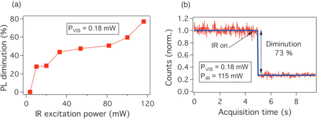
In order to use this IR pulsed excitation effect for different applications, it is iimportant to know what is the minimum power of the IR excitation to induce the modification of the luminescence of NV color centers and what is the maximum diminution of the photoluminescence. We have realized the measurement of the luminescence modulation as a function of both IR and green irradiating powers. The result shows that the quenching effect was not influenced much by the green power change, though lower green power allows to have better modulation. Whereas the change of IR power varies strongly the modulation of the luminescence of NV color center. Figure 3.8(b) shows the normalization of the luminescence signal as a function of the IR power. A threshold of about 5 mW is indicated, and the best modulation is about 73 % when PIR=116 mW as shown in Figure 3.8(a).
(a) (b) 80 60 40 20 0 PL diminution (%) 120 80 40 0 IR excitation power (mW) PVIS = 0.18 mW 1.2 1.0 0.8 0.6 0.4 0.2 0.0 Counts (norm.) 8 6 4 2 0 Acquisition time (s) IR on Diminution 73 % PVIS = 0.18 mW PIR = 115 mW
Figure 3.8: Photoluminescence quenching effect obtained by different IR excitation powers. (a) Normalized diminution of the luminescence as a function of IR power. (b) Photolumi-nescence as a function of time obtained without and with IR excitation, showing the best modulation.
Additionally, we observed that when we use high IR excitation power and for a long exposure time, the photoluminescence signal of NV color centers is unstable as shown in Figure3.9. Moreover, some of the luminescent centers irreversibly faded after several scans with strong IR light : a bleaching effect of high IR excitation power. This indicates that the strong IR excitation not only quenches the PL of NV color centers but also makes them blinking or even “kills” them under certain conditions. In combining with the observations shown in above, we propose that the PL quenching effect due to IR excitation is caused by the thermally induced variance of the environment around NV color centers. To clearify this point, we propose to study the IR excitation effect on the PL of NV color centers in a bulk diamond in which the NV color center is surrounded by a large area of diamond material. If the IR excitation induces some
3.4. Infrared excitation effect on PL of NV color centers in a bulk diamond 35 800 700 600 500 400 300 200 Counts/20ms 300 200 100 0 Aquisition time (s) IR excitation, PIR = 100 mW
Figure 3.9: IR quenching effect at high IR excitation power. The photoluminescence signal is unstable as a function of excitation time.
changes of the environment around NV color centers, we should have different results.
3.4
Infrared excitation effect on PL of NV color centers in
a bulk diamond
From the study of IR excitation effect of NV color center in nanodiamond, we know that the IR effect happens only when the IR pulses go after the VIS pulses, the un-stable character of NV color center under strong IR irradiation illustrates that the IR quenching effect is probably caused by the thermally induced variance of the environ-ment around NV color centers, such effect are supposed to be much more obvious on bulk diamond compared to nanodiamonds.
For the first test of the IR effect on the PL of NV color center in bulk diamond, the laser beam was focused slightly out of the sample surface. By switching on and off the IR beam, the modulation of the photoluminescence is immediately observed, similar to the observation on nanodiamonds. Figure 3.10 shows the IR effect as a function of the IR power. However, the modulation is not so high as in the case of diamond nanocrystals, even at very high IR power of about 360 mW. This doesn’t mean that the effective intensity is also high, because the focusing point is out of the diamond surface. This is only equivalent to an excitation of a large quantity of NV color center. Surprisingly, when we optimized the focusing point on the sample surface, the diamond in the focusing area is burned, indicating by an increase of the detected photon number from about 104 counts per second to about 106 counts per second. This photons are not related to the photoluminescence of NV color centers, but rather to emission of burned carbon atoms.
30 20 10 PL diminution (%) 300 250 200 150 100 50 IR power (mW) PVIS = 180 mW (a) (b) (c) (d) 1.2 1.0 0.8 0.6 Counts (norm.) 8 6 4 2 0 Aquisition time (s) IR on PIR = 50 mW 1.2 1.0 0.8 0.6 Counts (norm.) 7 6 5 4 3 2 1 0 Aquisition time (s) IR on PIR = 150 mW 1.2 1.0 0.8 0.6 Counts (norm.) 8 6 4 2 0 Aquisition time (s) IR on PIR=250 mW
Figure 3.10: IR effect on the photoluminescence of NV color centers in bulk diamond. The results are obtained by focusing the IR beam slightly out of the surface of diamond sample. The effect is similar to the one observed with nanodiamonds.
6 4 2 0 y (µ m) 6 4 2 0 x (µm) (a) (b) (c) 6 4 2 0 y (µ m) 6 4 2 0 x (µm) IR irradiation 20x103 15 10 5 Counts (/20 ms) 40 20 0 Aquisition time (s) IR on IR off
Figure 3.11: IR effect on the photoluminescence of NV color centers in a bulk diamond. The IR pulses burn the diamond surface at very low power (40 mW). The burning effect is immediate and no diminution of photoluminescence signal is observed. (a) and (c): scanning pictures obtained before and after 40 mW IR irradiation. (b) photoluminescence as a function of the acquisition time. The moments of turning on and off of the IR pulses are indicated.
3.4. Infrared excitation effect on PL of NV color centers in a bulk diamond 37 6 4 2 0
y
(µ
m)
6 4 2 0x
(µm)
(a) (b) (c) (d) 6 4 2 0y
(µ
m)
6 4 2 0x
(µm)
IR irradiation 500 400 300 200 100Counts (a. u.)
20 15 10 5 0 Acquisition time (s) IR on Burning PL decreases 10x103 8 6 4 2
Counts (a. u.)
30 20 10 0 Acquisition time (s) IR on IR off
Figure 3.12: IR pulsed excitation effect on the photoluminescence of NV color centers in a bulk diamond crystal. (a) Photoluminescence image obtained by only a 532 nm excitation. (b) Photoluminescence intensity obtained with on and off of IR excitation. A burning effect is observed. (c) Zoom in of the photoluminescence intensity curve obtained in the beginning of the IR excitation, showing the thermal effect of the high intensity IR excitation: i) photo-luminescence signal first decreases, as in case of nanodiamond, and then rapidly increases due to the explosion effect. (d) Photoluminescence image obtained after burning effect due to IR excitation. A black spot is observed at focusing point of the IR excitation beam.
For the excitation power larger than 40 mW, we can observe the burning effect at every where of the sample surface, as shown in Fig. 3.11. When the IR power is decreased to 30 mW or 20 mW, this effect is sensitive to the sample surface quality, the focusing position, and also the exposure time. It is quite interresting to study the IR excitation effect at this range of IR power and we may find out the relationship of the burning effect and the photoluminescence quenching effect.
Figure 4.8 shows the IR effect with PIR = 30 mW. At this power, the burning effect is not immediately obtained for all the tested areas. In particular, for some ar-eas, a decrease of photoluminescence is observed before burning. The instant between the IRon−moment and the burning varies from area to area. This experiment demon-strates two behaviors of the IR excitation, PL quenching and diamond burning, which
![Figure 2.2: Phase diagram for carbon indicating main regions of pressure-temperature space in which diamond growth occurs [8].](https://thumb-eu.123doks.com/thumbv2/123doknet/14528008.723149/16.892.272.640.415.676/figure-phase-diagram-indicating-regions-pressure-temperature-diamond.webp)