HAL Id: hal-00014222
https://hal.archives-ouvertes.fr/hal-00014222
Submitted on 22 Nov 2005
HAL is a multi-disciplinary open access
archive for the deposit and dissemination of
sci-entific research documents, whether they are
pub-lished or not. The documents may come from
teaching and research institutions in France or
L’archive ouverte pluridisciplinaire HAL, est
destinée au dépôt et à la diffusion de documents
scientifiques de niveau recherche, publiés ou non,
émanant des établissements d’enseignement et de
recherche français ou étrangers, des laboratoires
Observation of individual molecules trapped on a
nanostructured insulator
Laurent Nony, Enrico Gnecco, Alexis Baratoff, Audrius Alkauskas, Roland
Bennewitz, Oliver Pfeiffer, Sabine Maier, Adrian Wezel, Ernst Meyer,
Christophe Gerber
To cite this version:
Laurent Nony, Enrico Gnecco, Alexis Baratoff, Audrius Alkauskas, Roland Bennewitz, et al..
Ob-servation of individual molecules trapped on a nanostructured insulator. Nano Letters, American
Chemical Society, 2004, 4, pp.2185-2189. �10.1021/nl048693v�. �hal-00014222�
ccsd-00014222, version 1 - 22 Nov 2005
Observation of individual molecules trapped
on a nanostructured insulator
L. Nony
1∗, E. Gnecco
1, A. Baratoff
1, A. Alkauskas
1, R. Bennewitz
2,
O. Pfeiffer
3, S. Maier
3, A. Wetzel
3, E. Meyer
1,3, and Ch. Gerber
1,41
National Center of Competence in Research ”Nanoscale Science”, University of Basel, Klingelbergstrasse 82, CH-4056 Basel, Switzerland
2Dept. of Physics, McGill University, 3600 University street, Montreal PQ, H3A 2T8
Canada
3Institute of Physics, Klingelbergstrasse 82, CH-4056 Basel, Switzerland
4
IBM Research Division, Zurich Research Laboratory, CH-8803 R¨uschlikon,
Switzer-land
Published in Nanoletters 4(11), 2185-2189 (2004) Abstract
For the first time, ordered polar molecules confined in monolayer-deep rectangular pits produced on an alkali halide surface by electron irradia-tion have been resolved at room temperature by non-contact atomic force microscopy. Molecules self-assemble in a specific fashion inside pits of width smaller than 15 nm. By contrast no ordered aggregates of molecules are observed on flat terraces. Conclusions regarding nucleation and or-dering mechanisms are drawn. Trapping in pits as small as 2 nm opens a route to address single molecules.
The adsorption of medium-sized (< 100 atoms) functional organic molecules on patterned surfaces has become the subject of intensive studies motivated by the prospect of hybrid molecular electronic devices [1]. The operation of such devices should be governed by the electronic properties of a single or, at most, of a few of the constituent molecules. With this goal in mind, numerous groups have used scanning tunneling microscopy (STM) to study a variety of organic molecules adsorbed primar-ily on metal surfaces [2, 3, 4, 5, 6, 7]. Besides atomic-scale spatial resolution, STM provides the means for an “accurate placement of molecules in appropriate position and orientation to form a device”[1]. However, as discussed in ref.[1], many hurdles remain on the way towards the development and the integration of useful molecular electronic devices. In particular, it is desirable to electrically isolate the device; this can be achieved using an insulating substrate. The extension of atomic-scale character-ization and manipulation studies to surfaces of insulators is therefore of high interest.
It is, however, quite challenging because STM can no longer be applied, unless one deals with ultrathin insulating films on metals as substrates [8]. A more fundamental motivation for such studies is to understand the delicate balance between intermolecu-lar and molecule-substrate interactions which determines the mobility and aggregation of molecules, as well as their eventual ordering on ionic substrates.
Since 1995 non-contact atomic force microscopy (nc-AFM), has proven capable of yielding images with atomic resolution on a wide variety of insulating surfaces [9]. This technique relies on a micro-fabricated tip at the end of a cantilever excited at its fundamental bending eigenfrequency [10]. Upon approaching the surface, the tip first senses an attractive force which decreases the resonance frequency. The negative
frequency shift, ∆f , varies rapidly with the minimum tip-distance, especially a few ˚A
away from the surface. When ∆f is used for distance control, contrasts down to the atomic scale can be achieved in ultrahigh vacuum.
Recently, the technique has been used to study molecules adsorbed on various surfaces [11]. But so far, only few results have been reported concerning molecules ad-sorbed intact on insulators, presumably owing to the high mobility of such molecules at room temperature [12]. Thus, in order to obtain ordered molecular arrangements with a definite orientation on insulating surfaces, it is mandatory to find means to lower the mobility of the molecules. In the present work, we report a nc-AFM study of chloro [subphthalocyaninato] boron(III) (SubPc) molecules confined on a modified KBr(001) surface in ultra-high vacuum (UHV) at room temperature. For the first time, an ordered arrangement of molecules has been directly observed on a nanostruc-tured insulator consisting of intentionally created rectangular pits acting as molecular traps.
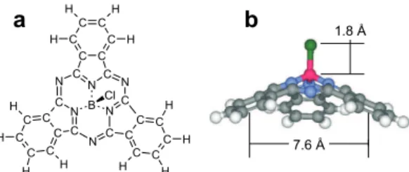
Cleaved alkali halide single crystals have been among the first insulating surfaces showing atomic periodicity and resolution of atomic-scale defects in nc-AFM exper-iments [13]. Clean flat surfaces can be rather easily prepared and imaged in UHV. Straight edged pits can be created by exposing the surface to an electron beam for a short time [14]. The pits are square or rectangular and one monolayer (ML), i.e. 0.33 nm, deep on KBr(001). First evidence for confinement, albeit without molec-ular resolution was found for flat PTCDA molecules [12]. Here, polar cone-shaped molecules are used. The chemical composition and structure of SubPc are shown in
figs. 1(a, b). The central boron atom is sp3
coordinated to an apex chlorine atom and to three isoindole moieties. The properties and potential applications of SubPc and related molecules have recently been reviewed [15]. The choice of this molecule has initially been motivated by its large dipole moment (5.4 D) pointing away from the protruding electronegative Cl atom which might form a strong ionic bond to sub-strate cations. Density functional theory (DFT) calculations predict a dipole moment close to the measured one and an electrostatically fitted effective charge of ∼ −0.4e on Cl [7].
The dynamic force microscope is a home-built instrument placed in a UHV
cham-ber with a base pressure of about 5 × 10⁻¹¹ mbar [16]. We used a silicon cantilever
with a supersharp tip [17] (resonance frequency f0= 165, 513 Hz, nominal spring
con-stant k = 48 N/m, quality factor Q = 30, 800). During the experiments, the tip is oscillating with a constant amplitude A ≃ 14 nm (±10% calibration uncertainty).
The KBr single crystal was cleaved in air, transferred to the vacuum chamber, heated to 393 K and irradiated with the 1 keV electron beam of a LEED electron source to produce the pits [18]. SubPc molecules were sublimed in UHV from a resistively heated aluminum oxide crucible while the sample was kept at 353 K and the pressure
Figure 1: SubPc molecule: (a) Schematic top view of the chemical structure; (b) Side view, with characteristic dimensions and atomic species (Cl: green, B: pink, N: blue, C: gray, H: white; from ref. [7]).
below 10−10mbar. A quartz-microbalance was used to calibrate the deposition rate.
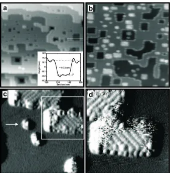
One ML of molecules was deposited, with an estimated error of about 20% [19]. Figure 2(a) shows a nc-AFM image of the KBr(001) surface at a constant fre-quency shift, ∆f = −10 Hz, after irradiation, but before deposition of the molecules. Monatomic steps and regular pits are clearly visible. Atomic resolution was obtained on flat (001) terraces at more negative ∆f ; as expected, only one type of ionic species was imaged as maxima [18]. Figures 2(b, c, d) show images of the sample after deposi-tion of 1 ML SubPc. Molecules and substrate ions could not both be resolved with the same ∆f , likely due to different force vs. distance characteristics [13]. The wide-area image in fig. 2(b) provides an overview of the way the molecules are distributed. They decorate steps and edges of wide pits, but only pits with a size smaller than 15 nm are filled (rectangular bright areas). No molecules are present on the flat terraces. In fig. 2(c), maxima attributed to single molecules can be recognized inside two pits and along their edges. The arrow indicates a 2 nm-wide pit trapping only 4 or 5 molecules. This is consistent with the nucleation mechanism described hereafter. In fig. 2(d),
the trapped molecules appear self-assembled into regular rows oriented +45o
(upper
pit) or −45o
(central pit) with respect to the edges. The distance between adjacent rows is 1.4 nm and the distance between two consecutive molecules in a row is 1.0 nm. The apparent height of the rows is about 0.6 nm with respect to the surrounding KBr(001) terrace, or equivalently 0.9 nm with respect to the bottom of the pit. The molecules are rather well-ordered in the center of each pits, but the structure appears somewhat mismatched along their edges. A blurred bright area attributed to mobile molecules and a few protruding molecules are also visible on top of the organized layer. When attempting to image at a more negative ∆f , thereby decreasing the tip-sample distance, horizontal stripes appeared, implying that material was dragged by the tip while scanning.
Let us consider the possible arrangement of the molecules inside the pits.
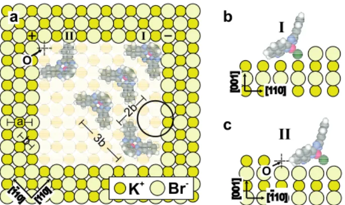
Fig-ure 3(a) shows that the alignment of SubPc’s in rows tilted ±45o
with respect to the [100] direction of the KBr(001) surface can match the underlying lattice if the distance between two adjacent rows is 3 × b = 1.40 nm and if two consecutive molecules in a row are separated by 2 × b = 0.93 nm, in good agreement with the experimentally observed spacings. However, this argument alone cannot explain why molecules are only found trapped within the smallest pits and not on the terraces. To address this question, we first discuss interactions of a single SubPc molecule with the substrate and then those between molecules. Intermolecular bonds are strong and no new
co-Figure 2: (a) Non-contact AFM image of the KBr(001) surface after electron irradiation (frame edge: 150 nm, ∆f = −10 Hz). Monatomic steps and pits, one layer deep, are visible. The bar indicates the location of the section shown in the inset. (b, c, d)- Non-contact AFM images of SubPc molecules on the electron-irradiated KBr(001) surface. (b) Frame size: 100 nm, ∆f = − 5 Hz. The molecules decorate steps and fill pits of width smaller than 15 nm. (c) Frame size: 27 nm, ∆f = −8 Hz. No molecules are observed on the KBr terraces. Molecular self-assembled structures are revealed within two pits. The arrow indicates a 2 nm-wide pit trapping a small number of molecules (4 or 5). The square denotes the scanning area shown in (d). (d) Frame size: 18 nm, ∆f = −8 Hz. Molecular resolution reveals that the structures are tilted ±45o with respect to the pits edges. Images (c, d) were processed using a technique which enhances the molecular contrast.
Figure 3: (a) Possible schematic arrangements of SubPc molecules inside a pit consisting of 10×10×1 missing ions. The lattice constant of KBr is a = 0.66 nm, thus b = a/√2 = 0.467 nm. The distance between two molecules in the diagonal row is 2 × b ≃ 1 nm, while the distance between rows is 3 × b ≃ 1.4 nm, in accordance with the experimental data. The Cl apex atom is strongly attracted to the electrostatic potential well near the corner site (position I), resulting in a tilt of the molecular axis. Position II is energetically unfavorable. (b) and (c) Side view along the [110] and [110] directions showing the approximate orientation of the molecule in position I and II, respectively.
valent bonds are expected to form. We therefore treat each SubPc molecule as rigid and interacting only via electrostatic and Van der Waals plus steric interactions. The latter are described by Lennard-Jones 6-12 pair potentials, using UFF parameters and combination rules [20].
Steps and pit edges expose ions of alternating sign, thereby preserving overall charge neutrality. The resulting electrostatic potential φ therefore oscillates parallel to those edges with a period equal to the lattice constant a = 0.66 nm, as it does along [100] and [010] directions above a flat terrace. Laplace’s equation implies that this oscillating component decays exponentially in empty space. The ions exposed at the pit corners (see fig. 3(a)) induce an additional component which varies on the scale of the pit width, except close to the corners. These features are readily apparent in figs. 4(a-c) which display φ computed along [110], [100] and [001] directions
passing through the first missing K+ion in the upper left corner (point O in fig. 3(a)).
The potential was computed for an array of point charges ±e at unrelaxed positions of the ions, an approximation which is sufficient for the following semi-quantitative discussion. Note in particular the pronounced minimum (actually a 3D saddle point)
in fig. 4(a) caused by the three Br−ions next to point O.
The rapid variation of φ over molecular dimensions requires taking into account the charge distribution within a SubPc molecule. In order to describe electrostatic interactions, it is sufficient to approximate that distribution by partial atomic charges fitted to the electrostatic potential of an isolated molecule in a surrounding shell. So-called CHelpG charges [21] were obtained from a density functional computation reported in ref.[7]. The appreciable charge on the Cl atom (−0.42 e) leads to a strong attraction to the upper right corner for a molecule in position I in figs. 3(a,b), but is,
however, mitigated by the steric repulsion from the neighboring K+
Figure 4: Electrostatic potential inside the pit displayed in fig. 3(a) along lines passing through point O in (a) the [110], (b) the [100] and (c) the [001] direc-tions, respectively. The potential was calculated by summing up the Coulomb contributions of 100 × 100 × 100 alternating electrical charges ±e at the unre-laxed positions of the ions and subtracting the contribution of a 10 × 10 × 1 squared monolayer slab in the center.
account appropriate UFF radii, we estimate an electrostatic energy gain of about 1 eV for the Cl atom. Owing to the decay of φ and to the alternating signs of the charges on the more distant B, C and N atoms, their contribution is an order of magnitude smaller. Van der Waals attraction favors the adsorption of a SubPc molecule to the bottom of the pit via two of its isoindole “feet”and also its trapping in position I. The
resulting trapping energy is so large compared to kBT at room temperature that it
prevents a SubPc molecule from diffusing away. Therefore corner sites which expose
K+ ions can act as efficient nucleation centers for molecules like SubPc. In the center
of the pit, however, the modulation of φ is only 0.3 V. The corresponding corrugation of the potential energy surface is dominated by the electrostatic interaction of the
protruding Cl atom and leads to a barrier of about 0.15 eV, i.e. almost 6kBT. This is
still insufficient to prevent diffusion of a single molecule at room temperature over the time needed to image one (about 12 scanlines, each lasting about 1 s). Moreover, the bias introduced by the slowly varying φ component, apparent in figs. 4(a,b), induces a drift of a molecule adsorbed inside the pit towards position I or to the equivalent site on the opposite side of the diagonal. This implies that molecules trapped near
opposite corners should be rotated by 180o
, but this prediction is difficult to verify. Position II in figs. 3(a,c) is much less favorable for trapping because charges, or atoms, which contribute most to electrostatic or Van der Waals attraction are kept away by steric repulsion of the feet from the pit edges.
The previous estimates are qualitatively consistent with our observations, namely that no molecules are imaged on flat terraces, while they appear trapped along the edges of steps and of pits smaller than 15 nm. Besides, pits as small as 2 nm appear filled; judging from figs. 4, this width is sufficient for the required potential profile to develop. The close packing along different diagonals inside the two pits visible in fig. 2(d) can be rationalized if those pits expose ions of different sign at their bottom right corners.
In an attempt to understand the observed ordering, we calculated the interaction between two SubPc molecules, using the same CHelpG charges and UFF parameters. The molecules were aligned as in the row schematically depicted in fig. 3(a) with their Cl atoms and two feet constrained to be in Van der Waals contact with a plane. The intermolecular binding energy, which is largely dominated by the Van der Waals component, is only 0.1 eV at the distance 2b, but increases by another 0.2 eV if the
molecules are allowed to reach their equilibrium separation, namely 7.25 ˚A≃ 1.5b, i.e. implying a serious mismatch with respect to the substrate corrugation. Therefore the observed stable commensurate order inside pits of intermediate size is presumably the consequence of a complex interplay between electrostatic and Van der Waals interac-tions between the molecules, the bottom and the edges of the pit, which requires more detailed calculations.
In any case, intermolecular interactions favors the relative orientation of molecules in adjacent rows shown in fig. 3(a). Note that the image in fig. 2(d) reveals irregu-larities, in particular along the pit edges. Once a molecule is trapped at position I and additional molecules arrange according to the supposed structure, steric repulsion prevents perfect matching along the pit edges (cf. black circle in fig. 3(a)). This mis-match must introduce some deviations from perfect ordering even in the absence of irregularities in the pit structure itself. Compared to fig. 4(a), the larger modulation of φ seen in fig. 4(b) implies a sizable diffusion barrier ≃ 0.7 eV along the pit edge. This phenomenon, which is a specific property of steps on ionic crystal surfaces [12], might explain why molecules trapped along extended steps, e.g. at the edges of wide pits, appear poorly ordered.
In conclusion, the nc-AFM measurements and theoretical estimates indicate that molecules with a protruding atom or small moiety carrying an appreciable charge (ow-ing to electronegativity differences between constituent atoms) can be trapped inside few nanometer-wide pits created by electron irradiation on a KBr(001) surface. Keep-ing in mind the goals outlined in the introduction, the next challenge is to study the trapping of various molecules, ”molecular wires” in particular [3, 22], equipped with judiciously positioned polar groups on different nanostructured ionic substrates. In that connection, note that monolayer deep pits have been created on several alkali halide (001) surfaces and that their average number, size and separation can be con-trolled by adjusting the electron dose and the substrate temperature [14]. A further challenge would obviously be to achieve intramolecular resolution. For that purpose, beyond the difficulty of the immobilization of the molecules, the tip preparation as well as the use of small amplitudes [23] are two key issues that are currently under investigation.
The authors acknowledge the Swiss National Center of Competence in Research on Nanoscale Science and the National Science Foundation for financial support. They thank S. Berner (University of Uppsala), J.J. Kolodziej (Jagiellonian Univer-sity, Krakow), M. von Arx and L. Ramoino (University of Basel) for discussions and advice, D. Schlettwein and W. Michaelis from University of Oldenburg for provid-ing the SubPc molecules, R. Allenspach and R. Schlittler from IBM Zurich Research Laboratory for advice on the design of the molecular evaporator.
References
[1] C. Joachim, J. Gimzewski, and A. Aviram, Nature 408, 541 (2000).
[2] E. Umbach, K. Gl¨ocker, and M. Sokolowski, Surf. Sci. 402-404, 20 (1998).
[3] V. Langlais, R. Schlitter, H. Tang, A. Gourdon, C. Joachim, and J. Gimzewski, Phys. Rev. Lett. 83, 2809 (1999).
[4] M. de Wild, S. Berner, H. Suzuki, H. Yanagi, D. Schlettwein, S. Ivan, A. Baratoff,
[5] S. Barlow and R. Raval, Surf. Sci. Repts. 50, 201 (2003).
[6] F. Rosei, M. Schunack, Y. Naitoh, P. Jiang, A. Gourdon, E. Laegsgaard, I. Stens-gaard, C. Joachim, and F. Besenbacher, Progr. Surf. Sci. 71, 95 (2003).
[7] S. Berner, M. de Wild, L. Ramoino, S. Ivan, A. Baratoff, H.-J. G¨untherodt, H.
Suzuki, D. Schlettwein, and T. Jung, Phys. Rev. B 68, 115410 (2003).
[8] S. Schnitke, S. Messerli, M. Pivetta, F. Patthey, L. Libioulle, M. Stengel, A. DeVita, and W.-D- Schneider, Phys. Rev. Lett. 87, 276801 (2001).
[9] S. Morita, R. Wiesendanger, and E. Meyer, Noncontact Atomic Force Microscopy (Springer, Berlin, Germany, 2002).
[10] F. Giessibl, Rev. Mod. Phys. 75, 949 (2003). [11] cf. for instance Ch. 11, 12 and 13 in ref. [9]
[12] L. Nony, R. Bennewitz, O. Pfeiffer, E. Gnecco, A. Baratoff, E. Meyer, T. Eguchi, A. Gourdon, and C. Joachim, Nanotechnology 15, S91 (2004).
[13] cf. Ch. 5 in ref. [9]
[14] J. Kolodziej, B. Such, P. Czuba, F. Krok, P. Piatkowski, P. Strutski, M.
Szymon-ski, R. Bennewitz, S. Sch¨ar, and E. Meyer, Surf. Sci. 482-485 (2001).
[15] C.G. Claessens, D. Gonzalez-Rodriguez, and T. Torres, Chem. Rev. 102, 835 (2002).
[16] R. Bennewitz, A. Foster, L. Kantorovich, M. Bammerlin, C. Loppacher, S. Sch¨ar,
M. Guggisberg, E. Meyer, H.-J. G¨untherodt, and A. Shluger, Phys. Rev. B 62,
2074 (2000).
[17] Nanosensors, http://www.nanosensors.com
[18] R. Bennewitz, O. Pfeiffer, S. Sch¨ar, V. Barwich, and E. Meyer, Appl. Surf. Sci.
188, 232 (2002).
[19] We used a deposition rate of 0.25 nm/min during 2 min. This coverage approxi-mately corresponds to a full monolayer of the hexagonal close-packed superstruc-ture of SubPc on Ag(111) reported in Ref. [7]. A proportional-integral controller
implemented with LabViewTM
varies the current to keep constant the power input to the evaporator, thus giving a better reproducibility than deposition at constant current.
[20] A.K. Rapp´e, C.J. Casewit, K.S. Colwell, W.A. Goddard III, and W.M. Skiff, J. Am. Chem. Soc. 114, 10024 (1992).
[21] C. Breneman and K.B. Wiberg, J. Comput. Chem. 11, 361 (1990).
[22] D.H. Yoon, S.B. Lee, K.-H. Yoo, J. Kim, J.K. Lim, N. Aratani, A. Tsuda, A. Osuka, and D. Kim, J. Am. Chem. Soc. 125, 11062 (2003).
[23] F.J. Giessibl, S. Hembacher, M. Herz, Ch. Schiller, J. Mannhart, Nanotechnology 15, S79 (2004).
![Figure 4: Electrostatic potential inside the pit displayed in fig. 3(a) along lines passing through point O in (a) the [110], (b) the [100] and (c) the [001] direc-tions, respectively](https://thumb-eu.123doks.com/thumbv2/123doknet/14574185.728186/7.918.203.627.182.304/figure-electrostatic-potential-inside-displayed-lines-passing-respectively.webp)