HAL Id: tel-02131527
https://tel.archives-ouvertes.fr/tel-02131527
Submitted on 16 May 2019HAL is a multi-disciplinary open access
archive for the deposit and dissemination of sci-entific research documents, whether they are pub-lished or not. The documents may come from teaching and research institutions in France or abroad, or from public or private research centers.
L’archive ouverte pluridisciplinaire HAL, est destinée au dépôt et à la diffusion de documents scientifiques de niveau recherche, publiés ou non, émanant des établissements d’enseignement et de recherche français ou étrangers, des laboratoires publics ou privés.
Electronic Packages
Stephane Zanella
To cite this version:
Stephane Zanella. Creep Fatigue Interaction in Solder Joint Alloys of Electronic Packages. Mechanics [physics]. Université Paris-Saclay, 2018. English. �NNT : 2018SACLX102�. �tel-02131527�
Creep Fatigue Interaction in
Solder Joint Alloys of Electronic
Packages
Thèse de doctorat de l'Université Paris-Saclay préparée à l’Ecole Polytechnique
École doctorale n° 579 Sciences Mécaniques et Energétiques, Matériaux et Géosciences (SMEMAG) Spécialité de doctorat : Mécanique
Thèse présentée et soutenue à l’Ecole Polytechnique, Palaiseau, le 13/12/2018, par
Stéphane Zanella
Composition du Jury : Aude Simar
Professeure, UC Louvain, Belgique Président
Hélène Frémont
Professeure, IMS Bordeaux Rapporteur
Jean-Yves Buffière
Professeur, INSA Lyon Rapporteur
Véronique Doquet
Directrice de recherche CNRS, Ecole Polytechnique Examinateur
Andrei Constantinescu
Directeur de recherche CNRS, Ecole Polytechnique Directeur de thèse
Eric Charkaluk
Directeur de recherche CNRS, Ecole Polytechnique Co-Directeur de thèse
Aurélien Lecavelier des Etangs-Levallois
Ingénieur Docteur, Industrie groupe Thales Invité
Wilson Carlos Maia Filho
Ingénieur Docteur, Industrie groupe Thales Invité
NNT : 20 18 S A C L X
Remerciements
Cette thèse a été réalisée dans le cadre d’une Convention Industrielle de Formation par la Recherche (CIFRE) entre l’équipe Technologies et procédés de l’Industrie groupe Thales et le Laboratoire de Mécanique des Solides de l’École Polytechnique.
Je remercie dans un premier temps Andrei Constantinescu, Directeur de recherche à l’École Polytechnique et directeur de cette thèse, pour m’avoir donné l’opportunité de réaliser cette thèse dans les meilleures conditions. Sa disponibilité et ses précieux conseils ont été indispensables à la réalisation de ces travaux.
Je remercie également Éric Charkaluk, Directeur de recherche à l’École Polytechnique, et co-directeur de cette thèse, de m’avoir fait bénéficier de son attention, ses idées ainsi que de son entière disponibilité dans ces recherches. Je n’ai cessé d’apprendre à ses côtés.
Je souhaite remercier Wilson Carlos Maia Filho, responsable de l’équipe Technologies et Procédés Thales, pour m’avoir fait profiter de son expérience et de m’avoir accordé sa confiance dans l’exécution des études. J’ai bénéficié de nombreux conseils éclairés et du meilleur cadre de travail.
Je souhaite également remercier Aurélien Lecavelier-des-Etangs-Levallois, Ingénieur de l’équipe Technologies et Procédés Thales, pour m’avoir accompagné dans cette thèse et de m’avoir partagé l’ensemble de ses clairvoyantes et astucieuses remarques.
Je remercie Hélène Frémont, Professeur à l’IMS Bordeaux, ainsi que Jean-Yves Buffière, Professeur à l’INSA Lyon, d’avoir accepté de rapporter cette thèse. Je leur suis reconnaissant d’avoir accepté de lire et revoir ce manuscrit.
Je tiens à remercier l’ensemble de l’équipe Technologies et Procédés, et plus particulièrement Damien Baudet, Julien Vieilledent, Arnaud Grivon, Julien Baudet, Ngoc Quach, Victor Chastand, Yann Tricot ainsi que Sourasith Souvannasot. Je remercie également Julien Perraud du laboratoire LAT-PI Thales et Charlotte Belloc qui m’a accompagné à un moment décisif.
Je tiens également à remercie grandement l’ensemble du Laboratoire de Mécanique des Solides, et en particulier Simon Hallais, Alexandre Tanguy, Vincent De Greef, Erik Guimbretière, Jean-Christophe Eytard et Pascal Marie.
Enfin, je remercie ma famille et mes amis. Leur présence a été mon meilleur atout dans la réussite de cette thèse.
Contents
Remerciements ... 3
Index ... 7
General introduction ... 8
Chapter I. Context and Objectives ... 10
1. Electronic boards ... 11
1.a. Aeronautic, space and defense critical markets ... 11
1.b. Electronic board structure ... 12
1.c. Electronic board assembly ... 14
2. Reliability of solder joints ... 15
2.a. Failure rate in time analysis ... 15
2.b. Stresses in solder joints during mission profile ... 16
2.c. Reliability challenges for critical applications ... 20
2.d. Prediction of solder joint failure with simulation ... 21
3. Mechanical properties of solder joints ... 22
3.a. Lead-Free solder joint microstructure ... 22
3.b. Elastic and plastic mechanical properties ... 23
3.c. Viscosity properties ... 31
3.d. Fatigue properties ... 35
4. Conclusions of the literature review and perspectives ... 41
5. Objectives ... 42
Chapter II. Experimental Setup ... 44
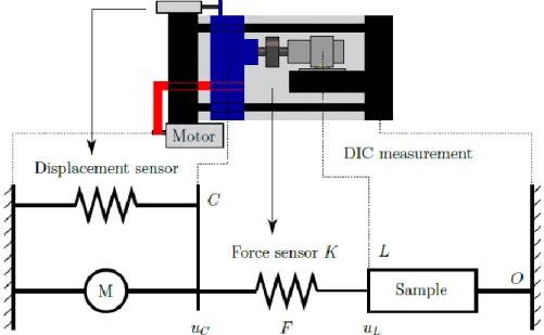
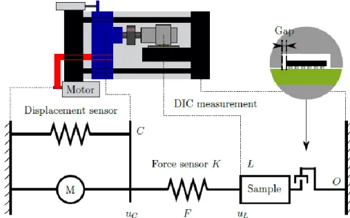
1. Innovative shear test bench ... 45
1.a. Shear test bench description ... 45
1.b. Samples of the shear test bench ... 46
1.c. Schematic representation of the shear test bench ... 47
1.d. Experimental results post-processing ... 48
1.e. Test in temperature ... 53
2. Accuracies of force and displacement measurements ... 55
2.a. Accuracy of the force sensor ... 55
2.b. Accuracy of the local displacement ... 57
2.c. Accuracy of tests in temperature ... 58
3. Monotonic tests ... 59
3.a. Results of the mechanical characterization ... 59
3.c. Residual stress for test in temperature ... 60
4. Step-Stress Results ... 61
4.a. Step-stress test ... 61
4.b. Step-Stress Results ... 62
4.c. Analysis of step-stress results ... 64
5. Conclusions ... 66
Chapter III. Failure Definition ... 67
1. Mechanical and electrical failures ... 68
1.a. Mechanical failure ... 68
1.b. Electrical failure ... 69
1.c. Specific configuration in this work ... 70
2. Criterion and mechanism of failure ... 71
2.a. Force and electrical resistance monitoring ... 71
2.b. Initial inspection ... 74
2.c. Failure mechanism during fatigue tests ... 75
2.d. Homogeneity of the loading ... 78
3. Mechanical parameters extraction ... 80
3.a. Methodology ... 80
3.b. Mechanical parameters for fatigue tests without dwell time ... 80
3.c. Mechanical parameters for fatigue tests with dwell time ... 84
4. Conclusions ... 87
Chapter IV. Fatigue Results ... 88
1. Fatigue tests ... 89
2. Test controls ... 90
2.a. Validation of experimental results based on selection criteria ... 90
2.b. Disturbance detected during the test... 90
2.c. Disturbance detected after post-processing ... 91
2.d. Test control synthesis ... 94
3. Results and discussions ... 94
3.a. Weibull distribution ... 94
3.b. Mechanical response ... 100
3.c. Damage indicators ... 103
3.d. Discussions ... 105
4. Conclusions ... 108
Chapter V. Cyclic damage analysis ... 109
1.a. Fatigue regimes ... 110
1.b. Importance of creep-fatigue interaction for solder joint alloys ... 111
2. Analysis of the results of the fatigue tests plan ... 112
2.a. Shear stress and strain ... 112
2.b. Inelastic strains ... 113
2.c. Simulation of the sample mechanical response ... 121
3. Creep-fatigue-interaction law for solder joint ... 122
3.a. Damage indicators synthesis ... 122
3.b. Damage law for solder joint material ... 123
3.c. Duration of dwell time ... 129
4. Conclusions ... 131
General conclusion ... 132
Bibliography ... 134
Annex 1: Résumé en français ... 140
Index
ATC Accelerated Thermal Cycling
BGA Ball Grid Array
CM Coffin-Manson’s fatigue law
COST Commercial Off-The-Shelf
CSP Chip-Scale Package
CTE Coefficient of Thermal Expansion
DIP Dual Inline Package
DoE Design of Experiment
EBSD Electron BackScatter Diffraction
EDX Energy Dispersive X-ray spectroscopy
FEA Finite Element Analysis
IC Integrate Circuit
I/O Input/Output
IPC Institute for Electronic Circuit Interconnects and Packaging ITRS International Technology Roadmap for Semiconductor
LF Lead-Free
DW Fatigue law based on dissipated energy per cycle
PCB Printed Circuit Board
PCBA Printed Circuit Board Assembly
QFN Quad Flat No-lead
QFP Quad Flat Package
RoHS Restriction of Hazardous Substances
SoC System-on-Chip
SiP System-in-Package
SoP System-on-Package
STD Standard Deviation
Tg Glass transition Temperature
General introduction
Solder joint ensures the electrical, mechanical and thermal links between electronic packages and the printed circuit board. As a result of external loadings, including temperature variation and vibration, and structural effects, solder joints of electronic products are submitted to stresses. Thus, from a reliability point of view on electronic boards, this makes them one of the most critical parts. For the aerospace and defense industries, the complexity with regards to guaranteeing the solder joints’ reliability in electronic products originates from a number of points including harsh environments, long mission profiles, as well as products’ high reliability specificities that are designed for these critical applications.
Printed Circuit Board Assembly’s evolution introduces new technology and materials that must be qualified for the aerospace and defense industries’ constraints. Within the study of solder joint reliability, it appears that the use of Finite Element Analysis simulation is a promising solution; one whose outcome is to maintain the increasing costs of qualification tests. However, mechanical properties of alloys used for solder joints are required for such simulation. So far, there is no significant consensus in the literature regarding mechanical constitutive models, parameters or fatigue laws. The mechanical behavior of these alloys is complex due to their low melting temperature and the visible viscosity domain is reached even at room temperature. Moreover, the creep fatigue interaction cannot be neglected in the fatigue analysis of these alloys. Therefore, it becomes apparent that the solder joints’ microstructure in the final application is nothing but complex.
The small size of solder joint, that being hundreds of micrometers, induces a small number of grains per solder joint. In addition, the assembly process induces intermetallic phases between the joint and the copper pads. Moreover, the shape of the solder joints is defined during the assembly process and therefore cannot be predicted. Subsequently, the assembly process of electronic packages introduces variabilities that change the mechanical properties of the alloy and the package in the final application. It is of course imperative to consider the final microstructure of the alloy when the mechanical properties of these alloys are studied through experimental tests.
When predicting lifetime, fatigue laws such as Coffin-Manson, based on the inelastic strain per cycle, as well as others based on the dissipated energy per cycle, are commonly used in the industry. Plastic and viscous strains are mingled in these laws and formulated as a total inelastic strain, thus supposing that damages from plastic and creep strains are comparable. Therefore, the relevance of these laws in the case of solder joint and the mission profiles of aerospace and defense industries are to be discussed. Important viscous strains are in fact developed due to not only a harsh environment within high temperatures, but also the mission profiles’ long maintain phases. In order to address such critical applications, the creep-fatigue interaction must be taken into account with regards to the fatigue law for solder joint alloys.
The objective of this thesis is therefore to define a fatigue law for assembled solder joints of electronic package which takes into account the creep-fatigue interaction.
Chapter one provides the general context of the study and identifies that there exists a lack of clear and precise experimental data to calibrate a fatigue law for solder joint in in-service representation conditions. Chapter two explores the development of an innovative test bench whose objective is to perform fatigue shear tests of assembled packages. Chapter three deals with the failure criterion and the importance of electrical resistance monitoring, and this is demonstrated through a fatigue test plan being performed with the test bench. Its aim is to evaluate the influence of force, temperature and
dwell time parameters. Chapter four then provides the results of these tests and finally chapter five focuses on the calibration of a creep-fatigue law.
Chapter I.
Context and Objectives
This chapter introduces the reliability of solder joints taking into account the constraints of aerospace and defense industries. The discussion starts with a description of electronic boards from a mechanical point of view. Specific role of solder joints is highlighted. Moreover, starting from the constraints of service loading and environment the mechanical stresses within the solder joints are reported.
The presentation of the subject continues with a literature review of mechanical properties of solder joints. The survey starts with the specific microstructure of solder joint and focuses then on their mechanical models. Elastic, plastic and viscous properties of solder materials are introduced for leaded and lead-free solder materials. The discussion emphasizes temperature and strain rate dependencies of the parameters and models as they play an important role under the prescribed service load conditions. Finally, fatigue results are presented both as the used criteria and applied lifetime predictions. The overview covers both classical fatigue criteria currently applied in industry as well as more complex models including damage evolution.
The literature review highlights that: (i) most material characterizations have been performed only on bulk samples, (ii) experimental setup rarely allows separated measurement of plastic and viscous strains and does not compare their relative impact on the mechanical and fatigue behavior of the solder joints and (iii) important scale effects are present in all physical phenomena under consideration analysis. The evolution of microstructure of the solder joints depends on several parameters and therefore the analysis of mechanical properties cannot be only performed by standard experiments on bulk samples. Moreover, this is accompanied by a shortage of precise experimental data which permit the definition and calibration of a fatigue law at the scale of the solder joint.
1. Electronic boards
This section introduces the reliability of solder joints taking into account the constrains of aerospace and defense industries. Electronic boards are described in detail taking into account the global structure and its constitutive elements and materials. The Manufacturing process of electronic packages is recounted next and the implication for reliability are highlighted. Finally, the actual challenges for the reliability of solder joints for critical applications are introduced in a critical discussion.
1.a. Aeronautic, space and defense critical markets
Electronic boards are nowadays part of numerous daily used products: computer, mobile, car, home automation systems etc. and generate a large number of technological developments. Consumer electronics market, mainly driven by smartphone applications, requires strong and constant miniaturization effort associated to functional performance increase for high volume, low cost and mild environments applications. A large number of new technologies are therefore developed to reach higher interconnection density of electronic boards. Commercially available electronic packages are also mainly developed for this market. These new technologies and packages are interesting for critical applications. However, reliability is a critical aspect for applications such as commercial avionics, transportation, space and defense. Integration of such new packages and technologies requires to qualify their use with the constraints of critical markets: high reliability, harsh environment and long mission profiles. In addition, if required, the need must be highlighted to apply strengthening strategies or to restrict their use to applications in less severe environment.
Products developed for space, defense and avionics industries have low production volume (10-10,000 pieces/year). Due to the high cost of each electronic board and the efficiency requirement, packages also need to be able to be repaired after failure. Furthermore, products lifetime is longer for these applications than for consumer electronics. In this context, it is critical and meaningful to study end-of-life reliability and electronic board mechanical behavior. For example electronic equipment embedded in a satellite needs to resist more than thirty years with a failure acceptable level smaller than 0,001% (see table for illustration Figure 1). The markets classification is based on a proposition from the American industry association IPC (Institute for Electronic Circuit Interconnects and Packaging)-SM-785 standard [1].
Figure 1: Specific needs of space, defense and avionics industries [2]
1.b. Electronic board structure
Electronic boards are used to perform complex functions in larger systems. Electronic boards are basically composed of a Printed Circuit Board (PCB) on which electronic packages are assembled with solder joints (see Figure 2), and are connected to other systems with connectors. The assembled electronic board with its packages is called Printed Circuit Board Assembly (PCBA).
Figure 2: Electronic board assembled with a Ball Grid Array (BGA) Package
Electronic packages are composed of a silicon die, a substrate and the molding. The silicon die is programmed with algorithms to perform specific calculations and is connected to the package substrate. This connection is the First-Level Interconnects. The substrate, which can be assimilated to a PCB, connects outputs of the die to the solder joints. Substrate has a laminate structure with copper layers and laminates, which are composite material with resin and glass fibers. More details about laminates are given in the following paragraph dedicated to PCB materials.
Solder joint ensures the electrical link between electronic packages and the PCB (Second-Level Interconnects). Electronic packages are connected to perform complex functions. Solder joint maintains also mechanically electronic packages on the PCB. Silicon dies heat up during use. Solder joints are also used to dissipate this heat. Solder joint types are generally classified according to the form of their attachments on the board. In fact, these connections types have a direct impact on packages reliability because failure often occurs in interconnections. Figure 3 illustrates this classification. Understanding the packages structure is important to build relevant numerical models of board for simulation purpose.
Electronic board Electronic package Matrix of solder joints
Encapsulation
Printed Circuit Board
First-Level Interconnects Second-Level Interconnects
Figure 3: Classification for attachments of packages on PCB [3]
PCB main goal is to interconnect electronic packages together to create more complex functions. Historically, PCB where monolayer boards: only composed of a dielectric support with a single printed copper layer. PCB are nowadays composed of multiple copper and dielectric layers (laminates) alternatively stacked together. This multilayer structure of the PCB is required to due to the increasing interconnect density of nowadays electronic packages. Laminate layers are composite structure: matrix of resin is reinforced with fiber glasses. Resin content in the laminate is an important parameter to calculate laminate mechanical properties. Different natures of resins can be used as epoxy or polyimide resins. The resins, with Coefficient of Thermal Expansion (CTE) around 20 ppm/K, is reinforced with fiber glasses which gives to the laminate a CTE in the fiber direction around 13 ppm/K. This value must be considered as first order approximation. Calculation of PCB mechanical properties is complex and out of the scope of this thesis. Lot of parameters including PCB stack-up and resin content must be taken into account.
(a) PCB with packages footprints (b) Cross-section of the PCB Figure 4: PCB multi-layers structure of electronic board
PCB manufacturing process can be decomposed in four main steps. First step is the etching of copper layers to form lines and planes to interconnect packages according to the electrical scheme. Packages footprints are added in the two external layers for the assembly of the packages. Second step is the manufacturing of the multilayer structure by laminating the different copper layers with dielectric in between for insulation. Third, after lamination, the different copper layers are linked together by mechanical or laser drilling and copper plating of vias. This process is repeated several times to obtain the desired PCB stack-up. Finally, finish plating and solder mask are deposited on the
outer layers to preserve exposed copper of footprints from oxidation and to help for packages assembly.
1.c. Electronic board assembly
Solder joints are formed during the assembly of the electronic board. A schema with the principal steps and the temperature profile of the PCB during the assembly in presented in Figure 5. More precisely the assembly process consists of the following steps:
(i) Solder paste is deposited on PCB footprints by a screen-printing process, (ii) Package are deposited on top side with a pick and place loading arm.
(iii) The board is heated up in a reflow oven following a dedicated thermal profile.
The thermal profile reaches a peak temperature above the melting point of the solder and presents specific heating and cooling ramps to minimize thermal residual stresses. For double-sided PCB architectures, the process is repeated in order to assembly an additional series of packages on the other side of the PCB. The process is ended by a series of inspections and electrical tests to verify the final package assembly. A protective layer can be applied by conformal coating on the complete board, without adding further temperature constraints on the packages.
Let us further remark that several process parameters have a direct impact on the reliability of the solder joints and consequently on the entire PCB assembly. Residual stresses are an outcome of the different coefficients of thermal expansion and the temperature changes during the assembly as they can facilitate the opening or closure of cracks if they have a tensile or compressive character. Moreover, cooling speeds will determine the precise crystallization process of solder joints and influence as such their joint microstructure.
(a) PCBA assembly process (b) Thermal profil used for PCBA assembly process Figure 5: Electronic package assembly: (a) PCBA process and (b) used thermal profile
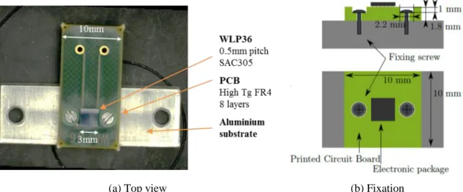
Assemblies from two distinct processes will be studied in the following chapters, (a) SAC305 using a free solder joint and (b) Backward SnPb+ using a containing alloy SnPb. If lead-free joints are the standard norm in the consumer electronics, the use of lead is still tolerated in critical applications as aerospace and defense. In the lead-free SAC305 assembly process, solder balls and
solder paste are made out of the SAC305 alloy. The SAC305 alloy is chemically composed of 3 wt.% of silver, 0.5 wt.% of copper and 96.5 wt.% of tin. The backward SnPb+ process, uses a solder paste made out of a leaded Sn37Pb alloy (37 wt.% of lead and 63 wt.% of tin), whereas the balls of the electronic package are made out of SAC305. Let us further notice that the solder joints of the Wafer Level Package (WLP) which will be discussed in chapter 2 contains 7 wt.% of lead after backward SnPb+ process. This value has been computed from the deposited quantity of solder paste. Up to date, aerospace and defense applications are not in the scope of environmental directives restricting the use of Lead.
Heterogeneity of assembly processes is a difficult and complex task from an industrial point of view. A low volume of production increases the relative cost of development and manufacturing and can justify the mixing of assembly technologies, which drives in itself the increasing cost. An example of the complexity of the assembly is the size of the package pitch, defined as the distance between two solder joints. Current electronic boards have packages with pitches in the range of 0.4 to 1.27 mm. Have this variety on an assembly line requires the existence of stencils with different thicknesses in different areas during the assembly process. As a consequence, the qualification of such an assembly process becomes very difficult and expensive.
2. Reliability of solder joints
Failure is a state of inability to perform a normal function. Reliability is the ability of a product to perform a under given conditions and for a specified period of time with an acceptable failure risk. Miniaturization and densification of electronic boards increase the risk of solder joint failure due for example to the induced reduction of solder joint sizes. Electronic boards structure and solder joint have been described in the previous section. The definition of reliability of solder joints will be now introduced. Mission profiles and induced stresses for solder joints will be presented. Accelerated reliability tests performed by companies to guarantee the reliability of solder joints will be detailed. Finally, some details about the use of simulation to predict cycles to failure in the context of solder joint will be given. Simulation is in fact an interesting solution to help reliability tests, understand failure mechanism and increase results from experimental tests.
2.a. Failure rate in time analysis
Let us now consider at a fixed time instant the instantaneous failure rate of a device. The evolution of the later with increasing time has proven to be a “bathtub” curve as described in [4]. In this representation one can identify three distinct phases characterized as (i) infant mortality, (ii) useful life also denoted as the “random steady-state” and (iii) end of wear or wear out (see Figure 6 for schematic representation).
The “infant mortality” corresponds to early failure and is associated to weakness created during or due to the manufacturing process. The reduction of this initial failure rate is generally harnessed through improvements in the quality control of the manufacturing process manufacturing and is not within the purpose of this work.
The “random steady-state” period characterizes the useful lifetime. In this period experience shows that failure occurs mostly random due to exceptional accidental loadings and has a low rate. Moreover, no evidence exists that would incriminate solder joints for the failures in this region (see [1] for a detailed discussion of this topic).
The “wear-out” region corresponds to the end-of-lifetime of the device under standard service loadings. It is characterized by a high increase of the failure rate and is a direct consequence of accumulating damage on different components. The detailed understanding of the subsequent damage mechanism and the precise distribution lifetimes corresponding to each failure mode are important for several reasons. On the one hand side they define the reliable life-time of the components and define inspect periods and non-destructive failure detection techniques and on the other hand side they permit to improve the component design and the assembly process by eliminating failure mechanism or by increasing lifetime through optimal design. It is obvious that in order to guarantee lifetime of the products engineers has to understand both service and exceptional loadings, or what is denoted in aerospace and defense applications the mission profile.
Figure 6: Failure rate bathtub curve [4]
2.b. Stresses in solder joints during mission profile
Electronic boards of space, defense and avionics products are used in harsh environment. Except manufacturing defects, corrosion and other chemical damage, there are three main sources of failure for solder joints of electronic boards: punctual mechanical shocks (during landing or operation for example), vibrations and large thermal variations [3]. Other environmental contributions, as corrosion or oxidation, induce damage mechanisms in solder joints but are not considered in the thesis. Manufacturers of critical markets need to guarantee long lifetime reliabilities in harsh environment for their products. If any failure occurs in the system, the consequences can be human casualties (for example in transport) or a huge financial losses (in satellite or space applications).
2.b.i. Mission profile analysis
Mission profile is the description of the product environment and the loadings submitted during the service. The environment loadings are described with physical quantities as temperature changes, vibration levels and relative humidity. An example of the daily temperature variations for two cities in different regions of the United States are represented in Figure 7 [5]. Possible mission profile definition for these two cities is highlighted by the two dotted lines. Red lines represent the maximum
and minimum temperatures and the blue line the most frequent cyclic stress. This analysis is presented as an example to illustrate how temperature variations from the environment can be evaluated. These temperature variations can describe for example the mission profile of a system which will be used in these cities. However, more investigations are required to evaluate the induced mission profile of the electronic boards of this hypothetical system.
Reliability of solder joint is qualified by manufacturers according to the product mission profile. However, it is not possible to perform 30 years of test before using technologies. Accelerated reliability tests are performed in order to evaluate the reliability of a product by subjecting it to conditions in excess of its normal service parameters. The equivalent lifetime in the field is predicted with accelerated test results and an acceleration factor (see Figure 8). These acceleration factors are estimated by engineers with the knowledges of fatigue properties of the considered component.
Figure 7: Temperature variation analyses for two US cities [5], red lines represent maximum and minimum temperatures and blues lines most frequently daily thermal changes
We recall the definition of failure mechanism as proposed in [6]:
“Failure mechanisms are the physical, chemical, thermodynamic or other processes that result in failure. Failure mechanisms are categorized as either overstress or wear-out mechanisms. Overstress failure arises because of a single load (stress) condition, which exceeds a fundamental strength property. Wear-out failure arises as a result of cumulative damage related to loads (stresses) applied over an extended time”.
Wear-out failure induced by cracks inside solder joint is the failure mechanism considered in this thesis. The failure mechanism during accelerated test needs to be the same as in the field. Prediction of reliability in the field is not possible if the failure mechanism during the accelerated test is not the same as in the field because the fatigue law may be different for another failure mechanism. Failure mechanism and fatigue law are important to compare test and operational environments and must be considered carefully.
Figure 8: Simplified schematic representation of the acceleration factor [4]
2.b.ii. Thermo-mechanical stresses
As previously introduced, temperature variations represent one of the failure sources of solder joints. The difference of thermal expansion between the PCB and the package induces stresses in the solder joints as illustrated in Figure 9 for a BGA electronic package. Due to the Coefficient of Thermal Expansion (CTE) mismatch, the principal direction of loading is shear strain. Tensile stress can also be observed by structural effect in particular for large package. Shear strain evolution as a function of temperature variation can be estimated with a simple analytical model. Considering 𝑙 the distance to the package center, ℎ the height of solder joint, and ∆𝛼 the CTE mismatch between the PCB and the package, the shear strain ∆𝛾 can be evaluated in the case of a ∆𝑇 temperature variation with the Eq. I-1. In this equation, the CTE of the PCB depends on the structure and the material used. The value given in Figure 9 (13 ppm/K) is approximative and is indicated for illustration. Equivalent CTE of the electronic package is lower than CTE of the PCB. One of the constituents of the package is the silicon die which has a CTE around 2.5 ppm/K [7].
∆𝛾 =∆𝛼 ∙ 𝑙 ∙ ∆𝑇
ℎ Eq. I-1
Accelerated Thermal Cycling (ATC) are used by manufacturers in order to evaluate solder joint reliability. The electronic board is submitted to a temperature profile, including dwell times at extreme temperatures. The amplitude of thermal variation is adjusted depending on the application. Thermal shock tests can also be used. The difference between ATC and thermal shock is the velocity of temperature variation. The temperature in the electronic board must be maintained homogeneous during the temperature variation for ATC. In the case of thermal shock, temperature variation rate is high, which conducts to thermal gradients. The rate limit which allows to maintain an homogeneous temperature depends on the technologies used. Dual chamber can be used for thermal cycling if the maximum temperature variation rate is lower than 20°C/min.
(a) (b) Figure 9: Loading state in the solder joints matrix of a BGA package induced by a temperature variation: (a) schematic view of the BGA package and loading of individual solder
joint and (b) linear evolution of the shear strain with temperature as modeled in equation Eq. I-1 (b)
2.b.iii. Mechanical stresses
Electronic boards are also submitted to mechanical vibrations transmitted by the operating system (as helicopter rotor) and by the environment (as road not perfectly plane). Mechanical shocks induced for example by missile launch are not considered in this study. Mechanical stresses are transmitted by the system to the electronic board inducing the bending of the PCB, and especially for frequencies around the resonant frequency of the electronic board where the bending of the PCB is high. Mechanical shear stresses are also induced in the solder joints by this bending as depicted in Figure 10, conducting to the high cycle fatigue regime.
Figure 10: Mechanical shear stresses induced by the bending of the PCB due to vibration loading from the environment of a BGA package
Drop tests have been introduced with the development of mobiles in order to evaluate the reliability of solder joint under mechanical shock. Mission profile of mobile application contains potential mechanical shocks. Drop tests are used to identify weakness and simulate drop.
Bending Electronic
package PCB
Fixations submitted to vertical vibration
2.c. Reliability challenges for critical applications
Evolution of electronic packages, mostly driven by consumer civil applications, introduces new architectures [8] and materials and their reliability needs to be qualified for the aerospace and defense applications constraints. Reliability of new package architecture, fatigue properties of Lead-Free alloys and use of reliable Commercial Off-The-Shelf electronic boards are today challenges of the aerospace and defense industries.
2.c.i. Architecture evolutions
Electronic evolution can be measured by the increase of integration level. This integration is visible in electronic packages which are smaller and more complex, with increased number of I/O (inputs and outputs) as BGA (Ball Grid Array) for instance. Figure 11 illustrates the densification phenomenon in terms of package sizes. Evolution of electronic packages from 1960 until now and densification and miniaturization of them is presented.
Dual Inline Package (DIP) is an electronic package composed of two lines of solder joints. Quad Flat Package (QFP) have four lines of solder joints (at each side) which increases the I/O density. Ball Grid Array (BGA) and Wafer Level Package (WLP) have been developed with a matrix of solder joints in order to maximize the package I/O density. Integration of several functions in the same package, “System-in-Package” (SiP), or in the same chip, “System-on-a-Chip” (SoC), or on the same package, “System-on-Chip” (SoP), allows to increase even more the density and the functionality of electronic packages. The increased number of I/O is only possible with a general reduction of the solder joint size which increases reliability risk.
Figure 11: Evolution of technologies and sizes of packages: miniaturization and densification of electronic packages [9]
2.c.ii. Lead-Free solder
Since the ROHS registration in 2002 (in application since 2006), the use of lead in electronic devices of consumer applications is prohibited. Historically, tin-lead Sn37Pb alloy were used for solder joint due to its low melting point and a good thermo-mechanical behavior. Lead-free (LF) solders have been selected as candidates to remove lead from electronic devices. They are generally
alloys based on tin (Sn) with different weight percent of silver (Ag) and copper (Cu). Knowledge on fatigue properties of these new alloys is important to guarantee the reliability.
2.c.iii. COTS
Use of Commercial Off-The-Shelf (COTS) electronic boards is attracting to reduce development costs and time-to-market. COTS are electronic boards designed in order to accomplish a specific or adaptable function for various applications. For example, a COTS electronic board can be composed of general functions as processor and memory with connections in order to be assembled in a more complex system. The advantage is the procurement of a low cost part which can be adapted to accomplish a specific function. Reliability of COTS is a source of concern. In fact, COTS are mostly dedicated to consumer markets with requirements different than aerospace and defense industries. Manufacturing process as assembly and selected technologies must be analyzed before a potential use in those applications. COTS electronic boards are also developed for aerospace and defense applications. However, it is difficult to justify their reliability without knowing their technologies. COTS manufacturers sell their electronic boards without giving the complete design.
2.d. Prediction of solder joint failure with simulation
Introduction of new electronic packages, printed circuit boards (PCB) and assemblies increases the qualification cost. In this context, the use of Finite Element Analysis (FEA) and numerical modeling in addition to experimental tests is a promising solution. In fact, simulation could improve our physical understanding of observed phenomena and increase the amount of information extracted from a given experimental test. For example, simulation of experimentally untested configurations can increase qualification cost efficiency.
A short overview of simulation models of the literature is proposed in this section. Regarding the prediction of solder joints reliability, literature is large and only examples for illustration are presented. Works of the literature can be organized regarding the complexity of the simulation (see Figure 12). Three categories are defined with simulation levels: (i) analytical formulations, (ii) FEA combining as beam and shell and (iii) complete 3D FEA using beam, shell and volume elements. Examples from the literature for each category are given in the following paragraphs.
Simplest empirical analytical models have been developed by Engelmaier [10] in order to evaluate a cyclic fatigue damage indicator during thermal cycling. The cyclic fatigue damage is formulated as function of first-order parameters. This cyclic fatigue damage can be used to calibrate a fatigue law based on experimental thermal cycling results in order to predict the failure. The advantage of this simulation level is the reduced computational effort.
Other simulations use simple elements as beam and shell. For example, the elastic response of a complete electronic board have been studied with beam elements for solder balls and shell elements for the PCB and the BGA package by Wong et al. [11] for a vibration loading. This approach has also been used by Massiot et al. [12] to simulate the stress and strain in the solder joints of a package submitted to ATC. This global model is used with a refined model of one solder balls and a part of the PCB in order to evaluate the cyclic stress and inelastic strain in the solder joint. Lower calculation times are required with this method and the complete electronic board is considered.
Simulation of thermal cycling does not necessary imply the simulation of the complete electronic board. Package symmetries can be used to propose reduced models. This third simulation category can use 3D FEA elements without exceeding limits of computation time. For example, 3D elements have been used to simulate the effective assembly stiffness of flip-chip solder joints [7]. This effective
stiffness has been re-used after with a solder joint model to evaluate creep strain developed in the solder joints during temperature variation. Crack growth during temperature variation has also been studied with 3D elements [13]. In this case, the strain energy density per cycle is computed and is combined with a crack growth rate model to predict fatigue life from crack growth data. This methodology has for example been used more recently to predict fatigue life of BGA solder joints under thermal cycling [14].
∆𝐷 =𝐹 ∙ 𝐿𝐷∙ ∆𝛼 ∙ ∆𝑇 ℎ with:
∆𝐷: cyclic fatigue damage 𝐹: deviation factor
𝐿𝐷: solder to center distance ∆𝛼: thermal expansion mismatch ∆𝑇: thermal range
ℎ: solder joint height
Engelmaier’s analytical model [10] (a)
Beam and shell model [11] (b)
3D elements model [14] (c)
Figure 12: Different simulation levels found in the literature: from empirical analytical models (a) to beam and shell elements model (b) and 3D complex elements model (c)
The condition to use one of these methods is the knowledge of the mechanical behavior and fatigue properties of the solder joints material. Mechanical and fatigue properties of solder joints have been studied by numerous authors. The following section reviews the literature regarding elastic and plastic, viscous and fatigue properties of solder joint materials.
3. Mechanical properties of solder joints
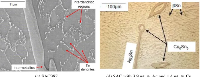
The characterization of mechanical properties of solder joints is performed with experimental tests based on different types of specimen. The following sections describe the works from literature regarding different mechanical properties. First, LF solder joint microstructure is depicted. A review of mechanical properties is then proposed. Leaded and LF solders properties are compared. Time-independent mechanical properties are described. These properties are the Young’s modulus, the yield stress and the ultimate tensile stress. Viscous properties are described after. Fatigue properties used for solder joints in the literature are finally detailed. The following annotation will be used. SACXYZ names a LF alloy which is composed of X.Y wt. % of Ag and 0.Z wt. % of Cu (the rest is Sn). For example, SAC305 is composed of 3.0 wt. % of Ag, 0.5 wt. % of Cu and 96.5 wt. % of Sn.
3.a. Lead-Free solder joint microstructure
SAC solder joint materials matrix is composed of a matrix of Tin elements in the β crystallographic form. The allotropic form of tin depends on the temperature (as described in Figure 13). The dendritic structure of the matrix is constituted of Ag3Sn and Cu6Sn5 precipitates formed during the assembly
process. Examples of LF SAC305 alloys microstructure are depicted in Figure 14.
Form 𝛼 𝛽 𝛾
Structure Face centered cubic Face centered tetragonal Orthorhombic
Representation
Figure 13: Description of cristallographic structure of tin as a function of temperature from literature [15] [16] [17]
Cooling rate of the reflow profile, solder volume and solder composition have an influence on solder joint microstructure [18]. These parameters are not independent from each other. Considering identical solder volume of samples, a coarsening of the dendritic structure has been observed for different SnAgCu alloys with the decrease of the cooling rate [19]. An Ag content above 3.5 wt.% causes the formation of large primary Ag3Sn precipitates [18]. Similarly, a Cu content above 1 wt.%
causes the formation of large primary Cu6Sn5 precipitates.
3.b. Elastic and plastic mechanical properties
Characterization of elastic and plastic properties is generally performed with monotonic experimental tests. These tests are commonly tensile or compression tests with bulk specimens. In the case of solder joint, because of the shear loading in the final application, shear tests have been performed in the literature. Elastic and plastic properties are represented in Figure 15. Young’s modulus describes the linear evolution of stress with strain in the elastic region until a yield and inelastic strains. Ultimate tensile stress is the maximum stress amplitude reached before failure.
Mechanical general properties of LF alloys have been analyzed by different authors. Evolution of mechanical properties with aging of LF solders is also a recurrent topic. Analysis of mechanical properties in high strain rate is also developed in the literature to evaluate the lifetime under mechanical loadings as vibration. Experimental methods used are first described. Elastic and plastic mechanical properties found in the literature are then compared in the last section.
(a) Alloy with Sn and 3.5 wt.% Ag (b) SAC387
Tin dendrites
(c) SAC387 (d) SAC with 3.9 wt. % Ag and 1.4 wt. % Cu Figure 14: Lead-free solder joint microstructure [20]: (a) optical image after chemical attack in order to reveal Ag3Sn intermetallic [21], (b) optical image of a BGA ball after cross-section [22], (c) SEM image of
the dendritic structure [22] and (d) constituents of solder joint material [23]
Figure 15: Elasto-plastic parameters measured defined with a schematic classic strain-stress response of material under tensile test
3.b.i. Elasto-plastic mechanical properties with different sample types
Most convenient specimens for tension or compression tests are bulk samples of the considered material. Figure 16 illustrates three types of bulk sample used in the literature. Vianco et al. [24] characterized the compression deformation response of SAC396 solder. Specimens are bulk samples machined in order to have cylindrical form with a height of 19 mm and a diameter of 10 mm. The strain/stress response of the samples is measured for a large temperature range from -25 to 160 °C and at different strain rates. Pang et al [25] [26] [27] have also used bulk samples for the SAC387 alloy. Cylindrical bulk specimens of Pang are thinner with a length of 15 mm and a diameter of 3 mm. The apparent Young’s modulus, the yield and the ultimate tensile stresses have been evaluated for different strain rates (from 5.6x10⁻⁴ to 5.6x10⁻²) and temperatures (25, 75 and 125 °C) by Pang et
al. Equations describing the evolution of these values are given as a function of these two parameters. Silver content impact has been analyzed by Che et al [28] with bulk of solders with different silver
Stress
Strain Real yield stress
Conventional yield stress
Ultimate tensile stress
: Young’s modulus
Intermetallics dendritesTin
Interdendritic regions
content (SAC105, SAC205 and SAC305). The specimen is a rectangular shape of 30 mm length and 3 mm thickness dog-bone shape. The solder alloys were melted 100 °C above their respective melting point for 20 minutes. The bulk solder specimens were casted inside the designed aluminum mold and naturally air-cooled at ambient temperature. Tensile tests have been performed by Che et al. at different strain rates and for different temperatures (from -35 to 125 °C). The elastic modulus, yield stress and ultimate stress limit of SAC solders are highly strain rate and temperature dependent. These properties increase with increasing strain rate, but decrease with increasing temperature. Elastic and plastic properties found are compared in the last section.
In order to be representative to the microstructure of the final application, mechanical tests with specific design of specimen have been performed in the literature as depicted in Figure 17. Pang et al. [27] have performed shear test on an assembled solder ball between two FR4 substrate materials of 12x3x0.5 mm3. Von-Mises equivalent stress criterion (see Eq. I-3) is used to obtain the relationship
between pure shear and pure tensile stress state in order to compare experimental results performed by Pang et al. with bulk and solder joint specimens. Interesting correlation between the yield stress and the ultimate tensile stress is found for the different temperatures and strain rates.
(a) (b) (c)
(a) (b) (c)
Figure 17: Specific samples used by Darveaux et al. [29] (a), Mysore et al. [30] (b), and Pin et al. [31] (c) in order to evaluate solder joint mechanical and fatigue properties
Von-Mises equivalent stress is used in order to express an equivalent stress scalar from a multi-axial stress state. The von-Mises equivalent stress 𝜎𝑒𝑞 is expressed as following with the Cauchy stress tensor components (𝜎11, 𝜎22, 𝜎33 are the stresses in the tensile principal directions and 𝜎12, 𝜎23, 𝜎31 are the stresses in the shear directions).
𝜎𝑒𝑞2 = 1
2((𝜎11− 𝜎22)
2+ (𝜎
22− 𝜎33)2+ (𝜎33− 𝜎11)2+ 6(𝜎232 + 𝜎312 + 𝜎122)) Eq. I-2 The relation between pure tensile stress 𝜎11 and pure shear stress states 𝜎23 considering the von-Mises equivalent stress is then
𝜎11= √3 𝜎23 Eq. I-3
Works of Bhate et al. [32] and Mysore et al. [30] are performed with dedicated specimens. The specimen consists in four solder interconnections located at the corners and “sandwiched” between two identical alumina substrates. The substrates are shear loaded at different temperatures (25, 75 and 125 °C) and for different strain rate (from 4.02x10⁻⁶ to 4.02x10⁻⁴ s-1) in order to characterize the
mechanical response of the four solder joints. The alloy studied by Bhate et al. is SAC387 and Mysore et al. SAC305.
Another specimen used in the literature is a thin layer of solder assembled between two rigid substrates. The microstructure and in particular the intermetallic layer with the copper pads can be respected with this type of specimen. The single lap shear of Pin et al. [31] is one example of this type of characterization. The mechanical response of the layer loaded in shear is measured and the shear modulus and the yield stress of the layer are defined at different temperatures.
3.b.ii. Mechanical properties evolution with aging
The evolution of the mechanical properties under specific conditions needs to be evaluated to guarantee the reliability of solder joint in some application domains. In this context, studies of the impact of aging at different temperatures have been performed for LF solders. Ma et al. [33] have observed that the material behavior evolution during thermal aging at room temperature and 125 °C is detrimental to the reliability with a reduction of stiffness, yield stress and ultimate strength and ductility. Specimens of Mustafa et al. have been manufactured with bulk samples of solders with a specific process in order to avoid residual stress and voids. Specimens have been prepared with a classic reflow profile to re-melt the solder in the tube using a vacuum suction process. The specimens used by Ma et al. are bulk rectangular specimens (80x3x0.5mm) of eutectic Sn37Pb or LF SAC405 solders. Mechanical properties evolutions with aging have been evaluated. Leaded and lead-free solders show different behaviors with aging. Mustafa et al. [34] [35] [36] have used the same process than Ma et al. with SAC105 solder and specimen of the same dimension. Effect of aging at 125 °C in cyclic strain or stress control response has been studied. Hysteresis response has also been analyzed with thin layer sample shear loaded. Evolution of the hysteresis area is used to evaluate the effect of aging, which induces changes of the yield stress and the ultimate strength. Fatigue tests have also been performed with this method and results are detailed in the following section. Effect of aging on mechanical properties has also been studied by Dompierre [20]. Bulks of solder (SAC305) with flat dog-bone shapes have been used to perform uniaxial and cyclic tension/compression tests. Dimension of the rectangular bulk is 20x13x3 mm3. As for other studies, the increase of the strain rate increases
the Young’s modulus and the ultimate tensile stress.
3.b.iii. Solder joint mechanical properties at high strain rates
Because of the dependency of mechanical properties on the strain rate, it is important to evaluate these properties even for high strain rate. In fact, an electronic board can be loaded with vibration at frequencies higher than 100 Hz. In this context, Lall et al. [37] [38] have studied the Young’s modulus and the ultimate tensile strength of lead-free SAC105 and SAC305 solders. The frequencies of the tests are sufficient to evaluate the solder at strain rates of 10, 35, 50 and 75 per second. Specimens are rectangular samples with a thickness of 0.5 mm. A dedicated experimental setup for the evaluation of the elastic deformation at high strain rates has been developed. As for Mustafa, the specimens have been submitted to an assembly reflow profile before testing in order to have a representative microstructure. The effect of aging on the properties has been characterized for different aging temperatures.
3.b.iv. Comparison of elastic and plastic properties from the literature
Elastic and plastic properties found in the literature are compared in this section. These properties are first compared regarding temperature. Then, evolution of properties with strain rate are compared at room temperature. Table 1 indicates color code used for the different solder joint materials found in the literature.
Table 1: Colors used to compare elastic and plastic properties of alloys from the literature Color
Evolution of the apparent Young’s modulus, yield stress and ultimate tensile stress with temperature are plotted in Figure 18, Figure 19, and Figure 20. Evolutions of these properties show a decrease of these properties with an increasing temperature, from room temperature to 200 °C. For temperature lower than 25 °C, no consensus exists on the variation of these properties.
Figure 18: Evolution of apparent Young's modulus with temperature
Figure 19: Evolution of plastic yield stress with temperature
The observed differences can be associate to the strain rate, the type of sample, the preparation and the test methods used. Different solders with different silver and copper content are also gathered in the same figure for LF solders. For the apparent Young’s modulus, evolutions of SAC305 alloy with temperature are different and can be explained by the difference of sample used.
For ultimate tensile stress and SAC305 alloy, the difference obtained at 25 °C by the two authors can be explained by the strain rate used. More creep strains are developed at lower strain rate which explains the lower ultimate tensile stress found at 10−3 than at 10 𝑠−1. For all temperatures, ultimate tensile stress for SAC105 and SAC387 is always lower than for SAC305.
Evolution of the elastic and plastic properties with strain rate are depicted in Figure 21, Figure 22 and Figure 23. In order to compare the results, only experimental tests performed at room temperature are plotted. For all alloys, an increase of the strain rate induces an increase of the apparent Young’s modulus, the yield stress and the ultimate tensile stress, which is due to the viscosity of the material.
Figure 20: Evolution of ultimate tensile stress with temperature
Figure 21: Evolution of apparent Young’s modulus with strain rate at 25 °C
Scatterings are observed for SAC305 alloys even if temperature and sample type used are identical. In this context, it’s difficult to compare the rigidity of SAC305 with other solder materials. Without viscosity, the Young’s modulus is expected to be constant with strain rate. The “apparent” Young’s modulus is measured based on experimental results without considering viscoelasticity.
Evolutions of Yield stress measured as function of strain rate are plotted in Figure 22. As for Young’s modulus, yield stress is not expected to change with strain rate if the viscosity of the material is taken into account. Yield stress are measured by these authors directly from the result without considering the viscosity. Scattering between yield stress obtained with double lap shear and bulk
0 10 20 30 40 50 60 70
1.00E-06 1.00E-04 1.00E-02 1.00E+00
A p p ar e n t Y o u n g' s m o d u lu s [M P a] Strain rate [1/s] 2002 SAC396 [24] 2004 SAC387 [25] 2006 SAC405 [33] 2006 SAC305 [33] 2006 Sn37Pb [33] 2012 SAC105 [34] 2010 SAC105 [28] 2010 SAC205 [28] 2010 SAC305 [28] 2011 SAC305 [20]
samples is more important for SAC305 than for SAC105 and SAC387. This difference is probably due to the methods used to calculate this parameter. Less scatterings are observed for experimental test performed with bulk samples. Experimental results show that viscosity for solder joint materials is important even at room temperature.
Figure 22: Evolution of plastic yield stress with strain rate at 25 °C
Figure 23: Evolution of ultimate tensile stress with strain rate at 25 °C
Evolution of Ultimate Tensile Stress as a function of strain rate for different solder joint materials is depicted in Figure 23. Two categories of experiments are depicted: at low and medium strain rates and at high strain rate (> 1 𝑠−1). Solder joint material characterization at high strain rate has been performed to evaluate properties for mechanical vibration loading.
Experimental tests performed at low and medium strain rates with high strain rate show an increase of ultimate tensile stress with strain rate for SAC305 and SAC105, values obtained for SAC105 being
0 10 20 30 40 50 60 70
1.00E-06 1.00E-04 1.00E-02 1.00E+00
Y ie ld s tr e ss [ M P a] Strain rate [1/s] 2002 SAC396 [24] 2004 SAC387 [25] 2008 SAC387 [32] 2008 SAC105 [32] 2009 SAC305 [30] 2010 SAC105 [28] 2010 SAC205 [28] 2010 SAC305 [28]
Double lap shear
Double lap shear
Bulk
Double lap shear
0 10 20 30 40 50 60 70 80
1.00E-06 1.00E-04 1.00E-02 1.00E+00 1.00E+02
U lt im at e t e n si le s tr e ss [ M P a] Strain rate [1/s] 2004 SAC387 [25] 2006 SAC405 [33] 2006 SAC305 [33] 2006 Sn37Pb [33] 2012 SAC105 [34] 2016 SAC305 [38] 2016 SAC105 [38] 2010 SAC105 [28] 2010 SAC205 [28] 2010 SAC305 [28] 2011 SAC305 [20]
lower than for SAC305. Evolution of ultimate tensile stress with strain rate is also due to the viscosity of the material. Viscous properties found in the literature are detailed in the following section.
3.c. Viscosity properties
Alloys used for solder joint are above half of their melting point at room temperature. In this context, creep processes are expected to dominate the deformation kinetics. Three regimes are described in the literature: primary transient creep (I), secondary steady-state creep (II) and tertiary creep (III). The different regimes are characterized by the creep strain rate. In the initial stage, the transient creep increases with a high strain rate but decreases with increasing time. Creep strain rate stabilizes to a constant value in the steady-state creep. Finally, the strain rate exponentially increases with time because of voids and cracks decreasing the loaded section of the specimen. The steady-state creep is the most studied regime in the literature with many proposed constitutive laws as the creep mechanism is function of the applied stress. Three main regions are described in the literature. The low stress regime (Nabarro-Heering creep) is the less developed. The intermediate (superplasticity) and high stress (climb controlled dislocation creep) regimes have been more studied. The literature regarding intermediate and high stress regimes is described in the following paragraphs.
3.c.i. Viscous properties characterization from the literature
Mysore et al. [30] have studied steady-state creep with the four corner solder joints specimen previously described (see Figure 17). Steady-state creep strain data have been obtained at 25, 75 and 125 °C and for different stress levels from 19.5 to 45.6 MPa. The solders considered are SAC305, SAC387 and SAC105. Norton’s law has been used with an additional factor to take into account the temperature effect (Arrhenius law) as formulated in Eq. I-4.
𝑑𝜀𝑐 𝑑𝑡 = 𝐴 ( 𝜎 𝜎𝑁 ) 𝑛 exp (− 𝑄 𝑘𝑇) Eq. I-4
𝑑𝜀𝑐/𝑑𝑡 is the creep strain rate. 𝜎 is the applied stress in Pa. 𝐴, in 1/s, and 𝜎𝑁, in Pa, are material constants. 𝑛 is the stress exponent. 𝑄 is the activation energy in J and 𝑘 is Boltzmann's constant in J/K. 𝑇 is the temperature in K. The parameters are calibrated on the steady-state creep data.
Influence of the stress on the strain rate formulation is different depending on stress level. At intermediate stresses, the strain rate depends on stress with the power law exponent 𝑛. At high stresses, an exponential impact of stress on the strain rate has been observed. This regime change is called power law breakdown and an unified expression is generally used corresponding to Eq. I-5, where 𝜎𝑁 is a material constant representing the power law breakdown.
𝑑𝜀𝑐 𝑑𝑡 = 𝐴 (sinh ( 𝜎 𝜎𝑁 )) 𝑛 exp (− 𝑄 𝑘𝑇) Eq. I-5
This formulation has been used by numerous authors to calibrate experimental results performed with bulk samples of solder alloy. Wiese et al. [39] have used dog bone-shaped bulk specimens with
a rectangular cross section (about 3x3 mm2) and a length of 60 mm (see Figure 24). Steady-state creep
strain rate data from 2 to 20 MPa stress levels and with temperatures from 20 to 150 °C have been used. The considered solders are LF Sn-40Pb-1.0Ag, Sn-3.5Ag and Sn-3.8Ag-1.0Cu. Pang et al. [26] have also used this law for the cylindrical bulk specimen of SAC387 previously described. Creep tests have been performed at -40, 25, 75 and 125 °C for different stress levels from 2 to 70 MPa. Xiao et al. [40] performed creep tests with rectangular bulk specimens of 12.7x1.58 mm2 and with gauge
length of 25.4mm of leaded Sn-37Pb and lead-free SAC396 solders. Steady-state creep strain rate data at 80, 115 and 180 °C and for different stress levels from 6 to 20 MPa have been measured.
(a) (b) (c)
Figure 24: Different samples type used in order to evaluate viscous properties of solder joint materials :thin layer [31] (a), flip-chip sample [39] (b), and electronic package [41] (c)
In order to be more representative of the microstructure, Zhang et al. [42] have performed creep tests with thin layer samples with strain rate form 10-11 to 10-4 s-1 and with temperature range from 20
to 180 °C. Viscoplastic constitutive properties of LF solder have been characterized with SAC396 solder and compared with eutectic Sn-37Pb. The specimen used by Zhang is a 3 mm length of thin layer of solder with a thickness of 0.18 mm between two shear substrates. Another specimen has been used by Röllig et al. [43]. This specimen is composed of four solder balls attached between two ceramic chips with adequate PCB pad metallization. Constant-load creep shear tests have been performed at different stress levels and temperatures (25, 75 and 125 °C) and parameters for the sinh-formulation have been defined for Sn-36Pb-2Ag, Sn-1.3Ag-0.2Cu-0.05Ni, Sn-1.3Ag-0.5Cu-0.05Ni and Sn-2.7Ag-0.4Cu-0.05Ni solders. The sample used by Darveaux [44] [45] [46] [29] is composed of two ceramic chips soldered with 98 solder joints (matrix of 10x10 joints depopulated of 2 joints). Two specimens are loaded in shear simultaneously by the test bench. Numerous solder types and pad metallizations have been tested under shear loading for different temperatures form -55 to 125 °C and stress levels form 1 to 30 MPa. Coefficients for the sinh-formulation are given by Darveaux and compared with other authors in the following section.
3.c.ii. Comparison of viscous properties of the literature
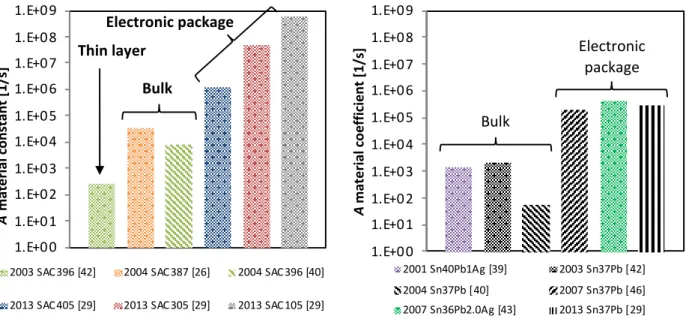
Parameters for the sinh-formulation found in the literature for the leaded and lead-free solders are summarized in the following Figure 25, Figure 26, and Figure 27. The comparison shows an important high scatter for the material parameter 𝐴 has a high scatter in the values found in the literature for leaded and lead-free solders. In the results presented for lead-free solders, the intermediate values obtained with bulk (Pang and Xiao) are surrounded by the lower value obtained by Zhang with thin layer sample and the matrix of solder balls used by Darveaux. The scatter of the results can be explained by the difference of test bench and used specimens.
The scatter found for the parameter 𝐴 is also found for 𝜎𝑁, as a lower value for 𝜎𝑁 can be balanced by a higher parameter 𝐴. For lead-free solders, the value measured by Pang with bulk specimen is close to the measured values of Darveaux for the different SAC solders. For leaded solders, the values of 𝜎𝑁 are significantly lower than those of lead-free solders.
Figure 25: A material constant for sinh-formulation for lead-free (left) and leaded (right) solders
Figure 26: σN material constant for sinh-formulation for lead-free (left) and leaded (right) solders
Values measured for the stress exponent 𝑛 have also a large scatter. For Xiao, the parameter has been set to 1 in order to eliminate this parameter from the calibration. This method can explain the difference between values obtained by this author. Globally, higher stress exponents are found for lead-free than for leaded solders.
1.E+00 1.E+01 1.E+02 1.E+03 1.E+04 1.E+05 1.E+06 1.E+07 1.E+08 1.E+09 A m at e ri al c o n st an t [1 /s ]
2003 SAC396 [42] 2004 SAC387 [26] 2004 SAC396 [40]
2013 SAC405 [29] 2013 SAC305 [29] 2013 SAC105 [29]
Thin layer Bulk Electronic package 1.E+00 1.E+01 1.E+02 1.E+03 1.E+04 1.E+05 1.E+06 1.E+07 1.E+08 1.E+09 A m at e ri al c o e ff ic ie n t [1 /s ] 2001 Sn40Pb1Ag [39] 2003 Sn37Pb [42] 2004 Sn37Pb [40] 2007 Sn37Pb [46] 2007 Sn36Pb2.0Ag [43] 2013 Sn37Pb [29] Bulk Electronic package 0 5 10 15 20 25 30 35 40 σN m at e ri al c o n st an t [M P a]
2003 SAC396 [42] 2004 SAC387 [26] 2004 SAC396 [40]
2013 SAC405 [29] 2013 SAC305 [29] 2013 SAC105 [29]
0 5 10 15 20 25 30 35 40 σN m at e ri al c o n st an t [M P a] 2001 Sn40Pb1Ag [39] 2003 Sn37Pb [42] 2004 Sn37Pb [40] 2007 Sn37Pb [46] 2007 Sn36Pb2.0Ag [43] 2013 Sn37Pb [29]
![Figure 17: Specific samples used by Darveaux et al. [29] (a), Mysore et al. [30] (b), and Pin et al](https://thumb-eu.123doks.com/thumbv2/123doknet/14744239.755658/27.892.154.731.103.471/figure-specific-samples-used-darveaux-mysore-and-pin.webp)