This is an author-deposited version published in: http://oatao.univ-toulouse.fr/ Eprints ID: 10735
To link to this article: DOI: 10.1016/j.sse.2012.11.005 URL: http://dx.doi.org/10.1016/j.sse.2012.11.005
To cite this version: Marcelot, Olivier and Magnan, Pierre Comparison
between TCAD simulated and measured carrier lifetimes in CMOS photodiodes using the Open Circuit Voltage Decay method. (2013)
Solid-State Electronics, vol. 81. pp. 135-139. ISSN 0038-1101
O
pen
A
rchive
T
oulouse
A
rchive
O
uverte (
OATAO
)
OATAO is an open access repository that collects the work of Toulouse researchers and makes it freely available over the web where possible.
Any correspondence concerning this service should be sent to the repository administrator: [email protected]
Comparison between TCAD simulated and measured carrier lifetime in CMOS photodiodes, using the Open Circuit Voltage Decay method.
O. Marcelot, P. Magnan
Université de Toulouse, ISAE, Image Sensor Research Team, 10 av. Edouard Belin 31055 Toulouse, France
Abstract
The control and the prediction of minority carrier lifetime are crucial for the design of
photodiodes, especially for CMOS image sensors, as signal electrons must be captured before recombination. Analytic models have been developed but do not allow accurate and reliable lifetime estimations according to complex photodiode architecture. In this work, we show for the first time that mixed mode TCAD simulations give accurate and reliable results on realistic photodiodes design. To achieve this conclusion, we have performed measurements and simulations on two different photodiodes using the Open Circuit Voltage Decay method.
1. Introduction
The recombination lifetime of photo-generated carriers is an important parameter in
photodiode design. Indeed, considering photo-generated carriers, we might wonder: in what time interval will the excess carriers recombine before being eventually captured by the cathode? This question is crucial in image sensors, especially if we want to realize very sensitive pixels. The recombination process at the origin of the signal carrier density decay is characterized by the carrier lifetime.
Maintaining a long recombination lifetime is crucial in the photo-detection, as we want to capture as much photo-generated carriers as possible in some areas, and avoid collecting them in others (e.g. to avoid crosstalk). It is thus necessary to measure and predict accurately the recombination lifetimes. In this way, recombination lifetime models have been developed. These models are based on high dopant concentration [1] (around 1x10¹⁷ at.cm-3) or on moderate dopant concentration [2, 3] (from 1x10¹⁴ at.cm-3). However, these analytical models are unsuitable for 2D/3D photodiode structures with various doping layers such as the one used in CMOS image sensors (Fig. 1).
TCAD simulations may become a solution to estimate the average lifetime in complex structure. In order to demonstrate that TCAD is reliable and a powerful tool in lifetime estimations, we propose here to compare recombination lifetime results with TCAD simulations.
Several lifetime measurement techniques have been studied [4-6], implying optical, or current excitations. As we want to characterize photodiodes, we have used the Open-Circuit-Voltage-Decay (OCVD) method. The OCVD technique was originally introduced by Gossick [7] and Lederhandler [8] in 1955. This technique involves the creation of excess carriers in a PN junction using a brief forward current excitation, and then a monitoring of the voltage across the junction after the abrupt termination of the excitation [7-14]. Then others authors changed the forward current excitation by an optical pulse [12, 15-17].
In the following, basics of the OCVD theory are presented in section 2, and then OCVD method is used to measure or to simulate photodiodes in order to extract carrier lifetimes in section 3. Discussions of the results are included in the section 3.
2. Summary of the OCVD theory
The junction voltage V(t) across the photodiode decreases when the excitation is switched off. It has been shown that the voltage expression as a function of time may be expressed as following [4, 8, 18]:
( )
( )
¸¸ ¹ · ¨ ¨ © § τ + ≈ r t erfc ln q kT V t V 0 (1)where is the recombination lifetime, and erfc(x) = 1 – erf(x) the complementary error function. This function shows a rapid decay followed by a linear slope. With the
approximation t greater than IJr the lifetime is deduced from the gradient of the V(t) vs t waveform, thanks to the following equation [4, 12]:
( )
t dt dV q kT r =− τ (2)which is derived under the simplifying assumption that recombination is dominated by quasi-neutral region recombination with the simple exponential voltage dependence exp(qV/kT). For the recombination in space charge region of forward biased junction, the dependence becomes exp(qV/nkT) where n is the diode ideality factor, between 1 and 2. Under high level injection, the lifetime is given by:
( )
t dt dV q kT 2 r =− τ (3)The high and low level injection curves usually show two different slopes [4, 11, 12, 18, 19], as illustrated in the Fig. 2.
3. Experimental results, TCAD and discussion 3.1 Forward current induced OCVD
N+P photodiodes have been fabricated using a 0.35µm process, with two different epitaxies on Czochralski (Cz) p-type wafers. The first epitaxy (sample A) is a 5 µm p-type silicon doped at 1.0x10¹⁵ B+/cm3 (see Fig. 1), and the second one (sample B) is a 10 µm p-type silicon doped at 1.0x10¹⁴ B+/cm3. The device under test is a 5.5 µm side square Nwell photodiode surrounded by Pwell.
The experimental set-up is shown in Fig. 3. The photodiodes are contacted with a Cascade prober which is connected to the MOSFET switch using coaxial cables.
In order to avoid any perturbation from the oscilloscope [12, 19], this experiment was performed with a unity gain buffer (TCL272), providing a very high input impedance of 1012Ohm.
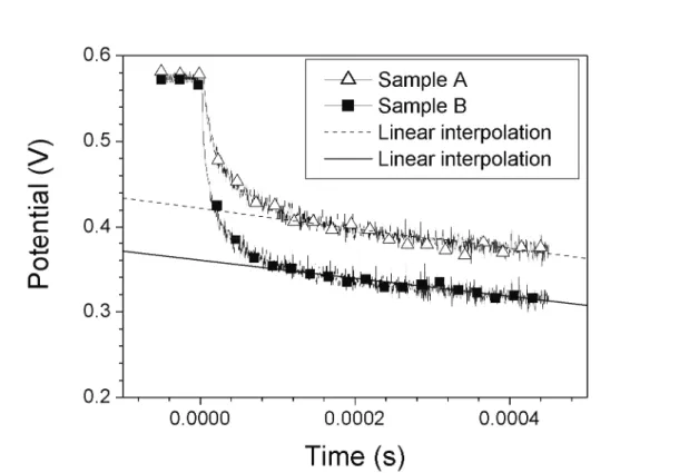
The OCVD results of the tested photodiodes are presented in the Fig. 4.
Both measurements show at t=0 a voltage step due to the ohmic voltage drop in the diode that is observed when the current flow ceases, as described by Schuster [20]. The voltage drop is more important on the sample B due to a higher resistive epitaxy. Then, a region of fast decay can be observed until t=100µs, which could be attributed to a high level injection regime [4, 6, 11-12] or to higher decay modes. Indeed, our samples are made of epitaxy and various layers, and the initial fast decay may be interpreted as a redistribution of carrier flows characterized by higher decay modes. After t=100 µs, the voltage decay vs. the time is
stabilized and linear, characterized by the effective lifetime. The lifetime computation is done in this part of the curve and gives the results listed in the Table 1.
The epitaxial layer the most highly resistive (sample B) gives the longest lifetime. The difference between the two samples is hardly visible because the Nwell area is surrounded by Pwell and only has its backside in contact with the substrate.
This experiment is simulated on the Synopsys Sentaurus environment, using the mixed mode of Sentaurus Device. The mixed-mode capability of Sentaurus Device allows for the
simulation of a circuit which can combine Sentaurus devices with other devices based on compact models (SPICE). The lifetime model used in Sentaurus is the one proposed by
Fossum in 1976 [2], and described by the following relation with IJn0=10-5 s and N0A=1016 cm-3:
(
)
A A n A n N N N 0 0 1 + τ = τ (4)This model was built from experimental measurement of lifetime as a function of resistivity of grown silicon ingots. In all simulations are activated the SRH recombination model with doping dependence, the “Auger recombination” model and the “surface SRH” parameter between silicon and oxide. The photodiodes are simulated from SIMS doping profiles in 2D to reduce computational time and memory constraints (Fig. 5). The photodiode anode is connected to a resistor Rs, connected to the source of an N channel MOS Transistor
(NMOST) which is the switch of our experiment. The spice parameters of the N-MOST are adjusted in order to keep the same ratio between N-MOST and photodiode capacitance in the TCAD study and in the experiment.
As in the experiment, we use Vd=0.6 V to polarize the photodiodes in the forward direction, and we apply a square pulse on Vg. Anode voltage versus time is plotted in the Fig. 6.
TCAD simulations do not reproduce the short voltage drop when the switch is turned off. This is due to the fact that the anode current is is low when the switch is turned off. Indeed, is in the range of nano-Ampere does not allow a visible voltage drop ∆V =is×Rs (Rs represents the
ohmic component of the circuit made of a resistor and of the MOSFET resistor). The anode current is is low because only one (instead of several ones in parallel) photodiode is simulated in 2D.
From the start to approximately 100 µs, a fast decay process is visible on both samples. In order to try to clarify the root cause by the fast decay process, two distribution profiles of the carrier recombination rates are plotted: 1 µs and 200 µs after the current extinction (Fig. 7), i.e. during and after the fast decay process. In the epitaxy layer, the carrier recombination rate is 100 times higher during the fast decay process than in the stabilized phase. It means that the fast decay is mainly due to a high level injection.
As in the experiment, the slope of the curve representing the sample A is higher during this regime. Regarding the sample B, the fast decay regime looks longer than in the sample A. Indeed, the lower slope of the curve is showing us a slower carrier recombination process which delays the stabilized phase.
In the stabilized and linear regime, the voltage decay is used to estimate the lifetime in a same way than in the experimental configuration (Table 1).
Simulated lifetimes are slightly underestimated by less than 20%. TCAD simulations give lifetime estimations in a good agreement with the experimental results, and it shows the good capability of TCAD to reproduce the forward current induced OCVD method.
3.2 Photo induced OCVD
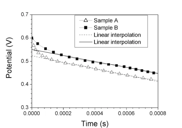
Measurements on same photodiodes are performed using the Cascade prober, however the excitation is replaced by a LED light. A white LED NSPW500BS is put in the cascade prober, above the tested chip. This LED has rise and fall times about 140 ns, and is fast enough to unable a lifetime measurement. As for the forward current induced OCVD the voltage across the photodiodes is measured using the unity gain buffer.
The LED is pulsed at 100 Hz and biased at 5 V. The measurement results are plotted in Fig. 8. On both samples, we may observe a very small voltage drop at the time of the light extinction. Then a fast decay regime is visible, which is longer on the sample B. After 100 µs, the curve slope is weaker and stabilized, and a lifetime estimation is performed, using a linear
interpolation (Table 2).The lifetimes measured are slightly higher compared to the ones measured with the forward current induced OCVD. Indeed, this photo induced method gives estimates of the carrier lifetime that are generally longer than those obtained from the forward induced OCVD [12, 19].
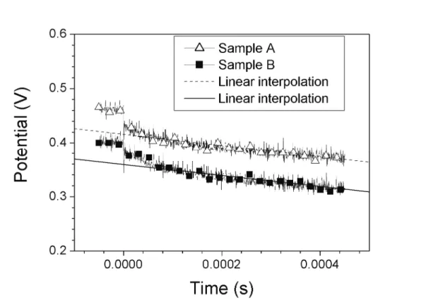
The experiment is as well simulated with the TCAD tools. The switch is connected to the anode of the photodiode, and Vgate=Vdrain=0 V. The photodiodes are illuminated with a 580 nm wavelength light at a power of 200 mW/cm². OCVD resulting curves are plotted in the Fig. 9.
At the extinction of the light, no voltage drop is visible as in the previous forward current OCVD simulation. Then, we observe a fast decay regime until 100 µs for the sample A and until 300 µs for the sample B. As in the previous simulation, the slope of the curve
representing the sample B is lower and involves a longer fast decay regime. Finally, the stabilized regime takes place and is used to estimate the lifetime. Some linear interpolations in the linear regime give the lifetimes in the Table 2.
Only a 6% mismatch on the lifetime estimation is visible: lifetimes estimations from TCAD simulations are quite in a good agreement with the experimental values. TCAD simulations
are able to reproduce the photo induced OCVD experiment and confirm that the Fossum model used in TCAD gives good approximation of carriers lifetime [2, 21] according to a complex 2D doping distributions.
4. Conclusion
We have successfully measured the minority carrier lifetime in CMOS photodiodes, using the OCVD method. The results show a limited increase of the minority carrier lifetime with the epitaxy resistivity because the cathode of the photodiode is surrounded by a Pwell. These experimental results were reproduced with TCAD tools using the mixed mode, and confirm the capability of TCAD to model the carrier lifetime in complex photodiodes. Both
simulation, of forward current induced OCVD method and photo induced OCVD method are in good agreement with experimental data and lifetime mismatch is less than 20% in CMOS photodiodes.
[1] S. E. Swirhun, Y-H. Kwark, R. M. Swanson, Electron Devices Meeting, 1986 International (1986), 32, pp. 24 - 27
[2] J.G. Fossum, Solid-State Electron. (1976), 19, pp. 269–277.
[3] S. W. Glunz, J. Lee, S. Rein, Photovoltaic Specialists Conference, 2000. Conference Record of the Twenty-Eighth IEEE (2000), pp. 201 -204
[4] D. K. Schroder, Semiconductor Material and Device Characterization, 2nd ed., Wiley-Interscience, New York (1998).
[5] D. K. Schroder, IEEE Trans. Electron Devices (1997), 44, pp. 160-170 [6] V. K. Khanna, Prog. Quantum Electron. (2005), 29, pp. 59–163
[7] B. R. Gossick, J. Appl. Phys. (1955), 26, pp. 1356-1365
[8] S. R. Lederhandler, L. J. Giacoletto, Proc. IRE (1955), 43, pp. 477–483 [9] L. Davies, Proc. IEEE (1963), 51, pp. 1637-1642
[10] S. Choo, R. Mazur, Solid-State Electron. (1970), 13, pp. 553-563
[11] R. J. Bassett, W. Eulop, C. A. Hogarth, Int. J. Electronics (1973), 35, pp. 177-192 [12] J. Mahan, T. Ekstedt, R. Frank, R. Kaplow, IEEE Trans. Electron Devices (1979), 26, pp.733-739
[13] D. Totterdell, J. Leake, S. Jain, Proc. IEE (1986), 133, pp. 181-184
[14] K. Joardar, R. Dondero, D. Schroder, Solid-State Electron. (1989), 32, pp. 479-483 [15] S. C. Jain, U. C. Ray, J. Appl. Phys. (1983), 54, pp. 2079-2085
[16] B. H. Rose, H. T. Weaver, J. Appl. Phys. (1983), 54, pp. 238-247 [17] B. H. Rose, IEEE Trans. Electron Devices (1984), 31, pp. 559-565
[18] J.E. Mahan, D.L. Barnes, Solid-State Electron. (1981), 24, pp. 989-949 [19] V. K. Tewary, S. C. Jain, Adv. Electron. Electron Phys. (1986), 67, p 329-411 [20] K. Schuster, E. Spenke, Solid-State Electron. (1965), 8, pp. 881-882
[21] J. G. Fossum, D. S. Lee, Solid-State Electron. (1982), 25, pp. 741-747
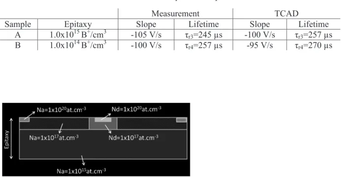
Table 1: calculated lifetimes from TCAD and experimental forward current-OCVD results
Measurement TCAD
Sample Epitaxy Slope Lifetime Slope Lifetime
A 1.0x10¹⁵ B+/cm3 -120 V/s IJr1=210 µs -140 V/s IJr1=184 µs B 1.0x10¹⁴ B+/cm3 -105 V/s IJr2=245 µs -130 V/s IJr2=198 µs
Table 2: calculated lifetimes from TCAD and experimental photo-OCVD results.
Measurement TCAD
Sample Epitaxy Slope Lifetime Slope Lifetime
A 1.0x10¹⁵ B+/cm3 -105 V/s IJr3=245 µs -100 V/s IJr3=257 µs B 1.0x10¹⁴ B+/cm3 -100 V/s IJr4=257 µs -95 V/s IJr4=270 µs
Fig.1: example of simplified CMOS image sensor photodiode unsuitable for analytic lifetime
Fig. 2: example of open-circuit voltage decay characteristic showing a high level and a low
level injection region [11].
Fig. 3: experimental read-out setup. A unity gain buffer is used between the oscilloscope and
Fig. 4: forward current induced OCVD on photodiodes on 1.0x10¹⁵ B+/cm3 epitaxy (sample A) and on 1.0x10¹⁴ B+/cm3 epitaxy (sample B). Linear interpolations are shown.
Fig. 5: TCAD circuit used to simulate the OCVD experiment. The photodiode is simulated
from SIMS profiles, and the NMOS is simulated from SPICE parameters. Vd=0.6 V, Vb=V_cathode=0 V.
Fig. 6: TCAD simulations of the forward current induced OCVD, and linear interpolations in
the stabilized phase. The switch is turned off at t=0 s.
Fig. 7: TCAD distributions of the carrier recombination rates of sample A (epitaxy 1.0x10¹⁵
B+/cm3). Left plot: 1 µs after the end of the forward current. Right plot: 200 µs after the end of the forward current.
Fig. 8: photo induced OCVD on photodiodes on 1.0x10¹⁵ B+/cm3 epitaxy (sample A) and on 1.0x10¹⁴ B+/cm3 epitaxy (sample B). Linear interpolations are shown.
Fig. 9: TCAD simulations of the photo induced OCVD, and linear interpolations. The light is
![Fig. 2: example of open-circuit voltage decay characteristic showing a high level and a low level injection region [11]](https://thumb-eu.123doks.com/thumbv2/123doknet/3528931.103288/8.892.107.535.101.451/example-circuit-voltage-decay-characteristic-showing-injection-region.webp)