OATAO is an open access repository that collects the work of Toulouse
researchers and makes it freely available over the web where possible
Any correspondence concerning this service should be sent
to the repository administrator:
[email protected]
This is an author’s version published in:
http://oatao.univ-toulouse.fr/24661
To cite this version:
Cure, Jérémy
and Piettre, Kilian
and Sournia-Saquet, Alix
and Coppel,
Yannick
and Esvan, Jérôme
and Chaudret, Bruno and Fau, Pierre
A Novel
Method for the Metallization of 3D Silicon Induced by Metastable Copper
Nanoparticles. (2018) ACS Applied Materials and Interfaces, 10 (38). 32838-32848.
ISSN 1944-8244
reducing stage of N,N′ diisopropylacetamidinate copper(I), named hereafter CuAmd. However, the ALD technique remains complex and difficult to master at the industrial level, and always requires an expensive equipment (secondary vacuum level, complex mastering of injection of vapor phases in the reaction chamber).12
To tackle these drawbacks, we present here a fully liquid implementation of an amidinate copper precursor as a response to thinfilms problems via the use of well controlled, colloidal metallic NPs.13In that aim, colloidal solutions of metal NPs may be considered as a reservoir of“metallic nano bricks”, which can be deposited on a substrate and ultimately form an electrically conductive metal layer.14However, the synthesis of colloidal solutions requires the use of organic ligands which“dress” the NPs, i.e., adsorb at their surface to stabilize them. Unfortunately, when these ligands are trapped in the metallic layer they are strongly detrimental to electrical conductance.15Therefore, the ligands should be temporarily active in order to stabilize copper NPs in solution, but eventually released in solution when NPs condense on the substrate, forming the thin film. Although highly desirable, this metallization sequence has never yet been described in metalfilm deposition processes. In this paper, we demonstrate this sequence via decomposition (under moderate temperature and H2pressure) of CuAmd in a toluene solution.
During this process, the decomposition of the precursor generates its own labile stabilizers (amidine moiety) which interact with copper nanocrystals in solution. Such“dressed” Cu NPs are metastable and the colloidal solution spontaneously evolves within few hours toward the condensation of a chemically pure, conformal, and conductive copper film on immersed surfaces. Moreover, this process allows the coating of high aspect ratio silicon structures (depth to entry ratio of 31) with a metallization ratio close to 100%. We have performed time resolved solution NMR experiments, UV−vis, TEM, SEM, and profilometry analyses to decipher the precursor decom position and thinfilm growth stages. These thin copper layers have been successfully employed as seed layers for electro chemically grown thick copper layers in narrow vias (aspect ratio of 3.5 and 10).
2. EXPERIMENTAL AND MATERIALS
2.1. Materials and Reagents. Si/SiO2substrates were supplied by
STMicroelectronics. The SiO2layer (1μm thick) is achieved through
wet oxidation and thermal growth on the silicon wafer. The substrates were cleaned in an ultrasonic bath with acetone and ethanol prior to use. Copper amidinate (I) precursor (N,N′ diisopropylacetamidinate copper(I), CuAmd) and toluene were purchased from Nanomeps S. A. and Sigma Aldrich, respectively. The solvent was dried using a purification system (Innovative Technology) and degassed by freeze/ pump steps in a Schlenk vessel. All experiments were conducted under a pure argon atmosphere using a glovebox and standard Fischer−Porter techniques.
2.2. Deposition of Copper Films. CuAmd precursor (50 mg, 0.08 mol/L) was introduced under a controlled atmosphere in a Fischer− Porter bottle with 3 mL of dry toluene. A Si/SiO2substrate (1× 2 cm)
was immersed in the toluene solution of CuAmd. The polished face of the Si/SiO2substrate was placed facing the bottom of the reactor in
order to avoid the deposition of precipitated copper aggregates. The unpolished backside of the substrate faced the solution surface. The Fischer−Porter reactor was then closed and pressurized with 3 bar H2
(Air Liquide Alphagaz 1 grade, purity 99.999%). Finally, the reactor was placed in an oil bath at the temperature of 110°C. The reaction was left running during the desired time. After 2 h, the metallization of the reactor walls was observed and the color of the solution was light red. At the end of the reaction, the reactor was quickly cooled and H2was
purged. The substrate, metallized on both faces, was rinsed in the glovebox with 2 mL of toluene and dried at room temperature under air. 2.3.1H NMR Characterization. Analyses were performed on a Bruker Avance 400 spectrometer for1H NMR and Bruker Avance 500
for DOSY experiments. Time resolved1H NMR was used to follow the
evolution of the reactive species during copper precursor decom position. The copper precursor in toluene solution under 3 bar H2at
110°C decomposes to yield metallic copper on the substrate. The evolution of copper precursor with time is determined by the integration of the singlet signal of the CH3 of the amidine group
located at 1.72 ppm and compared with the initial signal integration of the same group at t0 (seeFigure S1). The process was performed in a standard Fisher Porter reactor in toluene d8solvent. The reaction was
stopped at regular intervals in order to sample out 0.5 mL of the solution. All samples were introduced under argon atmosphere in the NMR tube at room temperature. In situ1H NMR characterizations
were performed in toluene d8in a dedicated NMR tube heated to 110
°C and pressurized with 3 bar H2.
Diffusion ordered spectroscopy experiments (DOSY) separate the NMR signals of different components in a mixture according to their diffusion coefficients. The rate of diffusion is inversely related to the molecular weight, size or shape of the molecule so that it is used to recognize each of the species in the solution. DOSY measurements were made using the stimulated echo pulse sequence with bipolar gradient pulses in toluene d8at 25°C. The diffusion dimension was processed
with the nonlinear least squaresfitting method (Topspin software). 2.4. Electron Microscopy. TEM images were taken with a Hitachi 7700 HT operating at 120 kV with a resolution of 2.3 Å (point−point) and 1 Å (line) at the Centre de Microscopie Electronique Appliqué à la Biologie (CMEAB, Toulouse). A drop of the colloidal solution was deposited on a copper grid for TEM observations. SEM images were taken on an ESEM Quanta 250field emission gun FEG operating at 200 kV with a resolution ranging from 1 to 3 nm at the CMEAB, Toulouse. The substrates were cut in 5× 5 mm squares and glued on an aluminum support with a silver paste before analysis.
2.5. UV−Visible Characterization. Colloidal copper nano particles are characterized by a localized surface plasmon resonance (LSPR) located around 580 nm, as evidenced by UV−vis spectrosco py.16The presence of nanoparticles in the reaction solution was studied with time on a PerkinElmer Lambda 25 spectrophotometer, at room temperature, between 400 and 1000 nm and using a quartz cell (L = 1 cm). A volume of 2.5 mL of the solution was introduced in a quartz cell under argon atmosphere to avoid the oxidation of copper nanoparticles. Time resolved UV−vis measurements were carried out by rapid cooling of the synthesis reactor to room temperature, then by collecting the supernatant sample for analysis.
2.6. XPS Characterization. X ray photoelectron spectroscopy (XPS) was used to analyze the chemical composition and determine the contamination level of copperfilms. XPS analyses were performed using a Thermoelectron Kalpha device. The photoelectron emission spectra were recorded using Al−Kα radiation (hν = 1486.6 eV) from a monochromatized source. The analyzed area was about 0.15 mm2. The pass energy wasfixed at 40 eV. The spectrometer energy calibration was done using the Au 4f7/2(83.9± 0.1 eV) and Cu 2p3/2(932.8± 0.1 eV)
photoelectron lines. XPS spectra were recorded in direct mode N (Ec). The background signal was removed using the Shirley method. The atomic concentrations were determined with an accuracy of 10% from photoelectron peak areas using the atomic sensitivity factors reported by Scofield, taking into account the transmission function of the analyzer. The binding energy scale was established by referencing the C 1s value of adventitious carbon (284.8 eV). Depth profiling of the copper layers was investigated by sputtering of the samples with Ar+
ions at 2 keV.
2.7. Cu Film Thickness Measurements. The thicknesses of Cu films were measured with a TENCOR P2 profilometer at the Atelier Interuniversitaire de Micronano Electronique (AIME), Toulouse. A protective photosensitivefilm was deposited on a part of the copper layer before the sample was immersed in a FeCl3 solution
film and create a step. The sample was rinsed with water and exposed to UV light for 3 min in order to remove the photoresistfilm.
2.8. Resistivity Measurements. The average resistivity of copper films was measured by a 4 tip resistivimeter at AIME facilities in Toulouse.
2.9. Electrochemical Cu Deposition for Filling of 3D Structures. The deposition of Cufilms was performed on a SiO2/Si
substrate covered with a thin MnSiO3barrier layer. The MnSiO3barrier
layer was deposited by a process developed in our team.17After Cu deposition, annealing was performed at 300°C during 3 h under a H2
flow to stabilize the copper layer. After these steps, the substrate was used as the working electrode for the electrodeposition of thick copper layer. Phosphorus doped copper was used as counter electrode in the electrochemical bath. The electrolytic bath, supplied by STMicroelec tronics, was composed of CuSO4·5H2O (55 g/L), NaCl (70 mg/L),
H2SO4 (50 g/L), and three additives (accelerator, leveler and
suppressor). The electrochemical cell was degassed prior to the electrochemical deposition. A constant current of −3 mA/cm was applied using a Autolab PGstat100 potentiostat/galvanostat purchased from Metrohm Autolab B. V. for 17 h. Finally, the substrate was rinsed by deionized water and dried under vacuum.
3. RESULTS
Colloidal NP synthesis in our group is based on the mild decomposition of metallorganic complexes in organic solvent with stabilizing ligands, under a moderate dihydrogen pressure (∼3 bar).18The copper deposition process presented here was inspired by the solution hydrogenolysis route for NPs synthesis, but with a major exception: the absence of any additional stabilizing agents. Recently, Cu NPs colloidal solutions were successfully prepared by the hydrogenolysis of N,N′ diisopro pylacetamidinate copper(I) (CuAmd), in toluene at 110°C in the presence of small amounts of fatty carboxylic acid or amine species.16,19 However, we observed that when no additional ligand is used, all other parameters being the same, a shiny copper film spontaneously formed after several hours on the glass walls of the reactor and on a silicon substrate placed in the reactor (Figure 1).
When other copper precursors like copper(II) iso butyrate (C8H14CuO4) or mesitylcopper(I) (C9H11Cu) are thermally
decomposed under H2 pressure, copper films form on the reactor walls as well. However, thesefilms either present a large amount of incorporated carboxylate ligands (in the case of the iso butyrate precursor), which lead to a very low electrical conductivity, or thefilms are heterogeneous and composed of poorly interconnected copper aggregates, detrimental to their electrical conductance.14 Surprisingly, only the use of the amidinate copper precursor leads to an homogeneous copper
condensation on the surfaces. To elucidate the deposition mechanism of this precursor, we performed a set of time resolved analyses of the reaction solution and of thefilm growth.
3.1. Characterization of the Reacting Solution and the Growing Film. Solution1H NMR. The silicon substrate and the
glass reactor walls initially present hydroxyl sites at their surface.20 CuAmd in contact with these surfaces may spontaneously react with the hydroxyl functions. In order to support this reaction scheme, the affinity of CuAmd with hydroxy groups was studied by1H NMR analyses and diffusion
ordered spectroscopy (DOSY) in toluene d8 at 298 K, in a
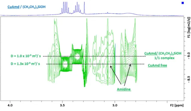
model reaction of a 1/2 mixture of CuAmd with triethylsilanol ((CH3CH2)3SiOH) (Figure 2 including the signals assign ments). The NMR spectrum of CuAmd/(CH3CH2)3SiOH
mixture showed a complex behavior. Notably, we evidenced the presence of free CuAmd (3 signals at 3.47, 1.75, and 1.22 ppm, D = 1.3 × 10⁻⁹ m2/ s), CuAmd in strong interaction with triethylsilanol in a 1/1 complex (3 signals at 3.35, 1.63, and 1.33 ppm, D = 1.0× 10⁻⁹ m2/ s) but also amidine molecules in interaction with triethylsilanol (Figure S2, 3 broad signals at 4.14, 3.06, and 2.87 ppm, D not measurable). Triethylsilanol shows two sets of resonances, a major one with a diffusion coefficient of D = 1.8 × 10⁻⁹m2/ s (2 signals at 1.14 and 0.68 ppm) that is lower than the free triethylsilanol one (2 signals at 0.98 and 0.52 ppm, D = 2.4× 10⁻⁹m2/ s) and a minor one with a
diffusion coefficient D = 1.0 × 10⁻⁹m2/ s (2 signals at 1.25 and 0.87 ppm) corresponding to the CuAmd/(CH3CH2)3SiOH 1/1 complex. These resonances correspond to triethylsilanol in fast exchange between free species and species in interaction with amidine molecules
Overall, 1H NMR and DOSY results strongly suggest that
CuAmd chemically interacts with silanol groups and may form adsorbed Cu complex on silicon substrates, but also that hydroxide groups can spontaneously decompose CuAmd and release free amidine. However, even with an excess of silanol as in our model reaction, unreacted and free CuAmd species remain in solution. Chabal et al.21have studied, by in situ FTIR technique, the interaction of the butylamidinate copper precursor [Cu(sBu amd)]2with hydroxylated SiO2substrates
during the ALD process, evidenced by the grafting of Si−O−Cu (sBu amd) species on the substrate. Similar results have been obtained by XPS analyses of ALD deposition of copper acetamidinate on SiO2 surfaces.22 These studies corroborate ourfindings on the reactivity of metal amidinate precursor with hydroxyl groups at room temperature.
Next, the reaction of CuAmd at 110°C under 3 bar H2was
studied by sampling the supernatant in a Fisher Porter reactor containing CuAmd at a concentration of 8× 10⁻²mol/L by1H
NMR in toluene d8 as a function of time (Figure S1). The spectra show the progressive disappearance of the proton signals corresponding to the CuAmd precursor and the appearance of a new set of proton signals corresponding to free amidine ligands. However, a latency period seems to precede the regular decomposition rate of the copper precursor. A new set of experiment were directly in a specialized NMR tube with an adapted copper concentration in order to avoid radiofrequency signal screening due to rapid metallization of the tube walls (6× 10⁻³mol/L). In this case, the consumption rate of the precursor in the NMR tube reveals a latency period up to ca. 10 min (Figure 3) before the precursor starts to decompose (precursor consumption <10%). After this induction period, the precursor decomposition evolves at a constant rate (1.4 × 10⁻⁴mol/L min) up to its total consumption after around an hour of Figure 1.Image of Cufilm mirror deposited on the reactor walls and on
silicon substrate (shown by arrow) by solution decomposition of CuAmd in toluene at 110°C (3 bar H2).
reaction. It is worth noting that at the end of reaction, the total amount of free amidine moiety in solution corresponds to the initial amount of amidinate in the precursor. This result suggests that there are no trapped amidine species in the deposited copper layer.
TEM. The TEM analysis of the supernatant recorded at different reaction time yields complementary results of the reaction evolution. After around 10 min, the solution turns light red which suggests the presence of Cu NPs. TEM analysis confirms the presence of well dispersed Cu nanocrystals with an Figure 2.(a)1H NMR and (b) DOSY analyses of (CH
3CH2)3SiOH (blue), CuAmd (red), and the mixture of both (green) in toluene d8.* The
DOSY peak of the CH3(SiOH) group of the CuAmd/(CH3CH2)3SiOH complex shows a diffusion coefficient higher than 1.0 × 10⁻⁹m2/ s because of
an overlap with a small and broad signal probably due to a labile OH/H2O hydrogen.
Figure 3.CuAmd precursor consumption during deposition process measured by in situ1H NMR ([CuAmd] = 6× 10⁻³mol/L). Inset right:
average size of 5.0± 1.0 nm (Figure 4a, b). These NPs start to aggregate in solution and form small blackberrylike structures after around 30 min. After 1 h, aggregates of ca. 20 nm surrounded by smaller NPs were found. After 3 h, most of the NPs in solution form ca. 40 nm large aggregates having probably undergone an Ostwald ripening process. At the end of the reaction, all the Cu NPs and aggregates have released their amidine ligands in solution after having being condensed as a solid statefilm.
SEM, Profilometry, and Conductivity. Simultaneously to NPs formation in solution, we observed the onset of a bright copperfilm on the reactor walls and on the substrate placed in the reactor. The growth of the metallic thinfilm is characterized
by SEM analyses taken at different reaction times (Figure 4c). For the short deposition times (10 and 20 min) the copper deposited on the substrate consists of adsorbed NPs or agglomerated NPs clusters (see zoomed image of 10 min Cu film in Figure S5). These observations confirm that the formation of NPs in solution is concomitant to the thin film growth on the substrate. With increasing time, the depositedfilm microstructure evolves toward larger copper nanostructures. The thicknesses of the copper layers measured by profilometry linearly increase with reaction time as shown onFigure 5a. The film growth stops after 3 h of reaction, i.e., when the precursor is fully consumed and all Cu NPs are condensed on the immersed surfaces yielding a layer with a thickness of ca. 220 nm. The Figure 4.Cu NPs formed at 10 and 30 min and 1, 2, and 3 h of reaction: (a) TEM images of Cu NPs in solution, (b) size distribution of NPs, and (c) SEM images of the Cufilm on the substrates.
resulting copper layer exhibits a resistivity of 5.3± 0.6 μΩ cm, which is only three times higher than the bulk copper one (1.6 μΩ cm).
UV−Vis Spectroscopy. UV−vis analyses confirmed the concomitant Cu NPs germination andfilm growth evolution (Figure 5b). Cu NPs display a localized surface plasmon resonance (LSPR) in the visible range, the position of which strongly depends on the nanoparticle aggregation.23The LSPR of colloidal copper formed after 10 min of reaction is located at 584 nm as expected for well dispersed and small size Cu NPs.24 With increasing reaction times, the LSPR red shifts and gets broader: after 2 h of reaction the NP absorption spectrum extends across the complete visible range as a result of their aggregation in solution. After 4 h, the supernatant is clear, and no residual copper aggregate remains in solution as indicated by the absence of any signal in the UV−vis spectrum.
In relation with the hard−soft acid−base theory, nitrogen atoms (hard base) may behave as even stronger ligands for copper than silver.25The interaction between amidine moieties and copper nanocrystals is large enough to yield Cu NPs in solution. However, owing to the small size of the amidine ligands and their dynamic exchange between the solvent and the metal surface,16 NPs remain in a metastable state. The first Cu nanocrystals in solution appear several minutes after the onset of the reaction as shown by TEM and SEM observations (Figure 4a, c). During this step, only a limited fraction of the copper precursor (<10%) is consumed as indicated by 1H NMR analyses. The presence of Cu NPs clusters on the substrate after 10 min (Figure 4c and Figure S5) provides evidence for the concomitance of NPs nucleation in solution and the initial condensation stage of Cu nanocrystals.
Copper Film Purity. After the Cu film growth on the substrate, a thermal annealing at 300°C was performed for 3 h under a H2 atmosphere to stabilize the film. Metallic layers
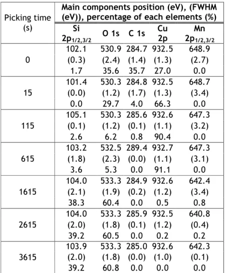
having high chemical purity is a major concern for conductive films since any chemical contamination may induce a degraded conductivity compared to bulk metal, or even bring undesired effects like reliability problems.26 The carbon content of the copper layer has been evaluated by X ray photoelectron spectroscopy (XPS) (Figure 6 and Table S1). XPS analysis reveals only traces of carbon found at the topmost surface of the sample, which may correspond to atmospheric carbon species and/or residual organic traces (solvent, ligands). After etching
the sample for 115 s, all the carbon from the surface pollution has disappeared and a residual level less than 0.8% is measured in the copper layer (Table S1 and Figure S6). After 615 s of surface etching, copper is at its maximum concentration and the carbon content is too low to be detected. It is noteworthy that no measurable signal of nitrogen species is detected on the sample even before sample etching, supporting the absence of trapped amidine ligands in the growing layer.
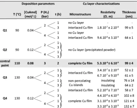
3.2. Influence of the Temperature, Precursor Concen-tration, Reducing Gas Pressure, and Time on the Cu Layer Growth. In order to master the growth of the Cufilm, we have investigated the role of the main parameters of the process. We set up an experimental matrix where temperature, precursor concentration, reducing agent pressure and reaction time are varied. These parameters are usually known to control the size and shape of metallic NPs prepared with stabilizers, and therefore they may play a pivotal role for the microstructure of the copper film. We explored values close to standard film deposition conditions, namely, a temperature of 110 °C, a concentration of 0.08 mol/L, 3 bar of H2, and decomposition
time of 2 h. In the experimental matrix, the temperature varied between 90 or 130°C, the precursor concentration from 0.04 to 0.12 mol/L, the H2pressure between 2 or 4 bar and the reaction time was 1 or 3 h. This resulted in a 16 experiments matrix (Table 1). A Si/SiO2substrate is placed in the deposition reactor for each experiment. Cu thinfilm microstructures are analyzed Figure 5.(a) Thickness of the deposited Cu layer on a SiO2/Si substrate at 10, 20, 30 min, and 1, 2, 3, and 4 h of reaction (dotted line is drawn as a
guide for the eye only); (b) time resolved UV−vis spectra of the reaction supernatant.
Figure 6.XPS elementary depth profiling of a copper film obtained on a silicon wafer (dotted line is drawn as a guide for the eye only).
by SEM, resistivity is measured by a four point method and thicknesses are characterized by profilometry.
The central point is characterized by a complete Cu film (Figure 7a) constituted of small copper grains leading to a
homogeneous layer aspect. Quarter Q1, corresponding to low temperature decomposition (90°C) and low copper concen tration (0.04 mol/L), leads to either the absence of a Cufilm or the formation of a discontinuous Cu film depending on the reaction duration (Figure 7c). In quarter Q2 (low temperature and high precursor concentration), no Cufilm is observed: a black precipitate of agglomerated Cu NPs forms at the bottom of
the reactor. The quarter Q3 (high temperature, low concen tration) leads to the formation of an incomplete Cu layer for the lower H2pressure, whereas isolated Cu islets (Figure 7d) form for the two others experiments (high H2 pressure). In these
latter cases, the discontinuity of the microstructure made of nonpercolating Cu islands gives rise to electrically insulating layers (Table 1). Quarter Q4 (high temperature, high concentration) yields complete and conductive Cufilms when the reaction time is 3 h and/or H2pressure is 4 bar (Figure 7b). These results clearly show that the process requires precursor concentration >0.04 mol/L and temperature above 90 °C (central point and Q4,Table 1) to achieve a full covering of the substrate by copper. The reaction time and hydrogen pressure influence the film formation in a secondary level. The high temperature conditions favor the rapid nucleation of Cu nuclei, thus overcoming the growth of larger nanoparticles in solution.27,28 If the temperature is too low, the formation of large copper aggregates is favored because initial copper nuclei are fed by a regular addition of precursor present in solution. When the aggregates reach a critical size, they precipitate at the bottom of the reactor and no copperfilm is formed. The second major reaction parameter is the precursor concentration because a minimum amount of Cu precursor is required to achieve a complete Cu layer. Experiments Q1 and Q3 with the lowest precursor concentration (0.04 mL/L), whatever the other parameters, always produce either no film, Cu islands or interlaced Cu films. These incomplete microstructures arise from a lack of sufficient matter to fully cover the immersed surfaces even if the reaction temperature is adapted. Taken together, the experimental data suggest the importance of Cu NP nucleation and their concentration in solution for fostering the production of a continuousfilm by metastable Cu NPs. Table 1. Matrix of Experiments and Characterization of the Cu Filmsa
aFor the sake of clarity, this experimental matrix has been organized into four quarters (Q1 to Q4, see Table 1) relying on the most important reaction parameters: temperature and precursor concentration. The thinfilm microstructures obtained with such an experimental matrix belong to four domains: no Cu layer (precipitated powder), nonpercolating Cu islands, interlaced Cu layer and complete Cu layer, i.e., full coverage of the surface (Figure 7).
Figure 7.SEM images of the Cufilm microstructure: (a) central point, (b) complete Cufilm, (c) interlaced Cu layer, and (d) nonpercolating Cu islands.
4. DISCUSSION ON THE GROWTH MECHANISM
1H NMR, UV−vis, TEM, and SEM characterizations of the
solution and the thinfilm allowed us to propose three major key stages of the copperfilms growth with time (Scheme 1): (i) adsorption of CuAmd on surface hydroxyl groups at room temperature and slow reduction stage under H2at 110°C; (ii)
regular growth stage by nucleation of Cu NPs in solution, condensation on surfaces, and release of free amidine; and (iii) formation of large clusters in solution and sedimentation. These major steps describing the growth process of the Cu thinfilm are detailed hereafter:
First Stage (Scheme 1, Steps a−c). As demonstrated by NMR studies, CuAmd in toluene solution at room temperature reacts with silanol groups present on the reactor walls and substrate surface to generate the very first adsorbed copper species. Because of the limited amount of surface−OH species, most of the copper precursor remains unaffected at this stage which corresponds to the steps a and b ofScheme 1. When the temperature is increased to 110°C and the reactor is pressurized under H2, the Cu species adsorbed on the surface are reduced to yield the veryfirst copper atoms. These copper atoms may act as favorable adsorption sites for the further growth of the copper layer driven by metal−metal interactions. Simultaneously, the homogeneous decomposition of CuAmd produces the colloidal copper nanocrystals in solution (step c of Scheme 1). Nanocrystal stabilization is facilitated via the labile amidine ligands released by the precursor decomposition. The interaction between metallic NP surface and amidine molecules has been previously evidenced in the case of silver NPs synthesized from silver amidinate precursor.19
However, during thisfirst stage, the decomposition of the Cu precursor is slow and corresponds to the induction period observed by1H NMR analysis, up to the point where enough
metallic copper is condensed on the surfaces to enable the second deposition stage.
Second Stage (Scheme 1, Step d). After this first induction period, the precursor starts to decompose at a regular speed. This stage corresponds to the fastfilm growth regime on the substrate. This onset seems to be triggered by a self catalytic decomposition reaction that occurs when the copperfilm grows on the immersed surfaces. Indeed, if the solution is removed from the NMR tube just after the onset of the fast decomposition regime and transferred into a clean NMR tube, the induction period recommences. A minimum amount of metallic copper has to be condensed on area surfaces in order to allow the fast decomposition of the CuAmd precursor. During this regime, Cu nanocrystals follow three main evolutions: they nucleate and grow in solution, where they possibly aggregate (Figure S4), whereas some of them regularly condense on the substrate (Figure 4b). This effect is confirmed by UV−vis spectra collected at different reaction times (Figure 5b). Between 10 and 30 min, the baseline of the absorbance spectrum increases in accordance with the concentration increase of Cu NPs in solution. After 30 min this concentration starts to decrease as a result of the condensation mechanism of Cu NPs on the substrate. In addition, the LSPR band gets larger and shifts toward the lower energy levels (i.e., bathochromic shifts) because of the aggregation of NPs with time.29,30Cu NPs spontaneously evolve in order to lower their Gibbs free energy by adsorbing onto any immersed surfaces (reactor walls and substrate). The metallic thinfilm growth is therefore fed by Cu NPs which evolve toward the maximization of Cu−Cu bonds in the condensed state compared to Cu−amidine bonds in solution. Each time a copper nanocrystal adsorbs on the surface, its amidine ligands are released as a free species in solution. The continuous increase of the amidine ligands in solution helps to stabilize larger Cu aggregates with time. Unlike the ALD process, the solution deposition mechanisms proceed by the incorpo ration of preformed Cu nanocrystals into the growing layer, releasing their labile ligands in solution, and leading to a clean copper layer.
Scheme 1. Schematic Description of Cu Film Growth Stagesa
a(a, b) CuAmd precursor initially adsorbs on the substrate at room temperature andfirst release of free amidine; (c) under 3 bar H
2and 110°C,
adsorbed CuAmd is reduced and NPs nucleation in solution occurs concomitantly; (d) regular growth of the layer by adsorption of NPs and NP clusters on surfaces and continuous release of free amidine ligands; (e)final step characterized by sedimentation of large Cu clusters on surfaces. Black, white, blue, and copper colored spheres represent C, H, N, and Cu atoms, respectively. Black arrows indicate the condensation of Cu NPs and clusters and the release of free amidine.
Third Stage (Scheme 1, Step e). During the third andfinal step most of the copper is already condensed as a thin metallic film and larger Cu grains may appear on the substrate (>3 h, Figure 4c bottom). Large Cu aggregates are stabilized in solution due to the availability of a high concentration of free amidine species. These amidine rich Cu aggregates do not undergo the previously described condensation mechanism on the growing layer but just settle at the bottom of the reaction vessel. These aggregates are considered as byproducts as they bring an undesirable amount of amidine ligands to the topmost surface of the Cufilm. They can be easily removed from the substrate by a simple rinse with solvent after reaction. One other way to avoid their presence on the substrate is to stop the reaction before they start to appear in solution by using shorter deposition times (between 1 and 2 h).
The solution decomposition of CuAmd under H2 allows
homogeneous coating of all immersed surfaces in the reactor by a thin and regular Cufilm. However, the deposition principle is based on the condensation of preformed Cu NPs or clusters of several nanometers large. It is therefore interesting to assess the ability of these Cu NPs or clusters to condense inside narrow and deep structures like silicon vias or trenches where geometrical constraints may count.
5. APPLICATION TO 3D SILICON FILLING
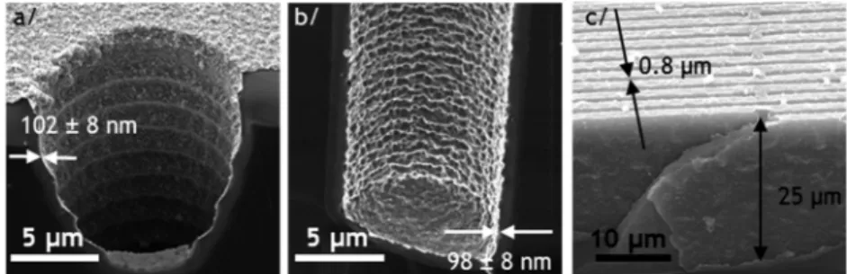
Beyond the interest of this process for Cu layer deposition on silicon substrates comprising a copper diffusion barrier17 (MnSiO3, seeExperimental and Materialssection), it has been employed on 3D silicon substrates presenting high aspect ratio structures like vias (depth and entry dimensions: 175−50 μm and 100−10 μm, aspect ratios of 3.5 and 10 respectively) or trenches (25−0.8 μm, aspect ratio of 31). Figure 8 presents cross section views of vias and trenches observed after ca. 100 nm Cu deposition at the central point conditions (Table 1). A continuous and conductive copper film is produced in these structures. The copper layer is conformal all along the walls and bottom of the vias, the thicknesses being very similar at the entry (102± 8 nm) and at the bottom (98 ± 8 nm) of the geometries (Figures 8a, b). The same observation applies for trenches which present a sub micrometer entry width where a thin and regular metallic covering of the walls is obtained (Figure 8c).
This conformal copperfilm formed into deep structures has been employed as a thin and conductive seed layer for the growth of thick copper by standard electrodeposition technique (seeExperimental and Materialssection). A constant intensity (−3 mA/cm) electrolysis process without stirring of the solution was performed.
The optical microscopy top view of the substrate before and after the electrochemical process reveals that all vias seem to be Figure 8.SEM images of silicon 3D substrate after 2 h of Cu deposition: (a, b) top view and bottom view of a 100μm deep and 10 μm wide via; (c) cross section view of trenches at 25μm deep and 0.8 μm wide.
Figure 9.Images of structured via substrate covered with Cufilm: (a) top view by optical microscopy before and (b) after electrochemically deposited thick Cu layer; (c, d) FIB SEM cross sectional images of (c) 175−50 μm and 100−10 μm vias (d) after thick Cu electrodeposition; (e−g) FIB SEM cross sectional images of the electrodeposited Cu inside a 100−10 μm via at the (e) top, (f) middle, and (g) bottom.
(11) Li, Z.; Barry, S. T.; Gordon, R. G. Synthesis and Characterization of Copper(I) Amidinates as Precursors for Atomic Layer Deposition (ALD) of Copper Metal. Inorg. Chem. 2005, 44 (6), 1728−1735.
(12) Brize, V.; Prieur, T.; Violet, P.; Artaud, L.; Berthome, G.; Blanquet, E.; Boichot, R.; Coindeau, S.; Doisneau, B.; Farcy, A.; Mantoux, A.; Nuta, I.; Pons, M.; Volpi, F. Developments of TaN ALD Process for 3D Conformal Coatings. Chem. Vap. Deposition 2011, 17 (10−12), 284−295.
(13) Green, M. Organometallic based strategies for metal nanocrystal synthesis. Chem. Commun. (Cambridge, U. K.) 2005, 24, 3002−3011.
(14) Barriere, C.; Alcaraz, G.; Margeat, O.; Fau, P.; Quoirin, J. B.; Anceau, C.; Chaudret, B. Copper nanoparticles and organometallic chemical liquid deposition (OMCLD) for substrate metallization. J. Mater. Chem. 2008, 18 (26), 3084−3086.
(15) Kanelidis, I.; Kraus, T. The role of ligands in coinage metal nanoparticles for electronics. Beilstein J. Nanotechnol. 2017, 8, 2625− 2639.
(16) Barriere, C.; Piettre, K.; Latour, V.; Margeat, O.; Turrin, C. O.; Chaudret, B.; Fau, P. Ligand effects on the air stability of copper nanoparticles obtained from organometallic synthesis. J. Mater. Chem. 2012, 22 (5), 2279−2285.
(17) Cure, J.; Piettre, K.; Coppel, Y.; Beche, E.; Esvan, J.; Colliere, V.; Chaudret, B.; Fau, P. Solution Layer Deposition: A Technique for the Growth of Ultra Pure Manganese Oxides on Silica at Room Temperature. Angew. Chem., Int. Ed. 2016, 55 (9), 3027−3030.
(18) Bradley, J. S.; Millar, J. M.; Hill, E. W.; Behal, S.; Chaudret, B.; Duteil, A. Surface chemistry on colloidal metals: spectroscopic study of adsorption of small molecules. Faraday Discuss. 1991, 92, 255−268.
(19) Cure, J.; Coppel, Y.; Dammak, T.; Fazzini, P. F.; Mlayah, A.; Chaudret, B.; Fau, P. Monitoring the Coordination of Amine Ligands on Silver Nanoparticles Using NMR and SERS. Langmuir 2015, 31 (4), 1362−1367.
(20) McCrate, J. M.; Ekerdt, J. G. Titration of Free Hydroxyl and Strained Siloxane Sites on Silicon Dioxide with Fluorescent Probes. Langmuir 2013, 29 (38), 11868−11875.
(21) Dai, M.; Kwon, J.; Halls, M. D.; Gordon, R. G.; Chabal, Y. J. Surface and Interface Processes during Atomic Layer Deposition of Copper on Silicon Oxide. Langmuir 2010, 26 (6), 3911−3917.
(22) Yao, Y.; Zaera, F. Thermal chemistry of copper acetamidinate atomic layer deposition precursors on silicon oxide surfaces studied by XPS. J. Vac. Sci. Technol., A 2016, 34 (1), 01A101.
(23) Chan, G. H.; Zhao, J.; Hicks, E. M.; Schatz, G. C.; Van Duyne, R. P. Plasmonic Properties of Copper Nanoparticles Fabricated by Nanosphere Lithography. Nano Lett. 2007, 7 (7), 1947−1952.
(24) Santillan, J. M. J.; Videla, F. A.; Fernandez van Raap, M. B.; Schinca, D. C.; Scaffardi, L. B. Size dependent Cu dielectric function for plasmon spectroscopy: Characterization of colloidal suspension generated by fs laser ablation. J. Appl. Phys. 2012, 112 (5), 054319.
(25) Nath, S.; Ghosh, S. K.; Kundu, S.; Praharaj, S.; Panigrahi, S.; Pal, T. Is gold really softer than silver? HSAB principle revisited. J. Nanopart. Res. 2006, 8 (1), 111−116.
(26) Dixit, V. K.; Neishi, K.; Akao, N.; Koike, J. Structural and electronic properties of a Mn oxide diffusion barrier layer formed by chemical vapor deposition. IEEE Trans. Device Mater. Reliab. 2011, 11 (2), 295−302.
(27) LaMer, V. K. Kinetics in phase transitions. Ind. Eng. Chem. 1952, 44, 1270−1277.
(28) Rueping, M.; Koenigs, R. M.; Borrmann, R.; Zoller, J.; Weirich, T. E.; Mayer, J. Size Selective, Stabilizer Free, Hydrogenolytic Synthesis of Iridium Nanoparticles Supported on Carbon Nanotubes. Chem. Mater. 2011, 23 (8), 2008−2010.
(29) Blakey, I.; Merican, Z.; Thurecht, K. J. A method for controlling the aggregation of gold nanoparticles: tuning of optical and spectroscopic properties. Langmuir 2013, 29 (26), 8266−8274.
(30) Mahapatra, N.; Halder, M. Facile reversible LSPR tuning through additive induced self aggregation and dissemination of Ag NPs: role of cyclodextrins and surfactants. RSC Adv. 2014, 4 (36), 18724−18730.
S-1
Supporting Information
A Nove
l Method for the Metallization of 3D Silicon
Induced by Metastable Copper Nanoparticles
J. Cure,ab K. Piettre,ab A. Sournia-Saquet,a Y. Coppel,a J. Esvan,c B. Chaudret,d P. Fau a*
a
LCC-CNRS, Université de Toulouse, CNRS, UPS, 205 route de Narbonne BP 44099, 31077 Toulouse, France.
b
STMicroelectronics SAS, 10 impasse Thales de Millet, 37070 Tours, France. c
CIRIMAT-ENSIACET, Université de Toulouse, CNRS, UPS, 4 allée Emile Monso BP 44362, 31030 Toulouse, France
d
LPCNO, Université de Toulouse, CNRS, INSA, UPS, 135 avenue de Rangueil, 31077 Toulouse, France
Corresponding author
S-2
Time-resolved 1H NMR analysis of CuAmd precursor consumption:
Chemical shift corresponding to the CuAmd precursor (400 MHz, 298 K, toluene-d8): δ (ppm) 3.44 (heptuplet, 4H, CH of isopropyl group, 3J = 6.2 Hz), 1.72 (s, 6H, CH3 of amidine group), 1.19 (d, 12H, CH3 of isopropyl
group, 3J = 6.2 Hz), 1.18 (d, 12H, CH3 of isopropyl group, 3J = 6.2 Hz).
Chemical shift corresponding to the amidine ligand (400 MHz, 298 K, toluene-d8): δ (ppm) 4.17 (bs, 1H, NH group), 3.45 (bs, 1H, CH of
isopropyl group), 2.91 (bs, 1H, CH of isopropyl group), 1.36 (s, 3H, CH3
of amidine group), 1.18 (bs, 6H, CH3 of isopropyl group), 1.02 (bs, 6H, CH3 of isopropyl group).
When the reaction is operated in NMR tube a lower concentration of CuAmd is employed (6.10-3 mol/ L) in order to avoid the complete metallization of the tube walls. The percentage of the CuAmd precursor consumption for a given time ta was determined by the integration of the
singlet signal of the CH3 of the amidine group located at 1.72 ppm and compared with the initial
S-3
Figure S1. Detailed 1H NMR spectra recorded during CuAmd hydrogenolysis in a Fisher Porter reactor ([CuAmd] = 8 x 10⁻² mol/ L).
S-4
Interaction between CuAmd and triethylsilanol evidenced by 1H NMR:
Figure S2. 1H NMR spectra of (CH3CH2)SiOH (blue), CuAmd (red), and the mixture of both (green) in
toluene-d8 in the range 4.8 to 2.2 ppm. Cuamd/SiOH correspond Cu complex in interaction with triethylsilanol. Amidine/SiOH corresponds to amidine released from the Cu complex and in interaction with ethylsilanol.
S-5
Figure S3. 1H DOSY NMR analyses in the domain 2.4 to 4.0 ppm of (CH3CH2)3SiOH, CuAmd and the
S-6
Figure S4. HRTEM image of aggregated Cu NPs in the supernatant after 2 h of CuAmd thermolysis
S-7
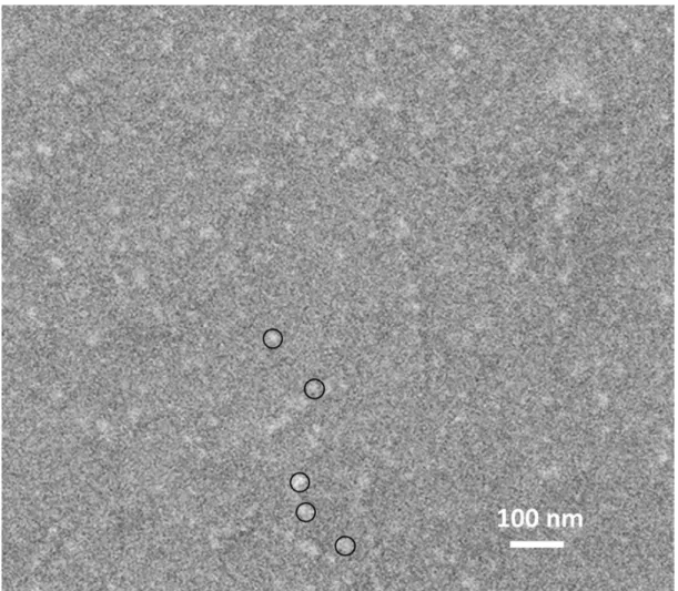
Figure S5. High magnification SEM image of 10 minutes deposited layer showing the microstructure of
ca. 30 nm features formed by adsorbed Cu NPs clusters on the substrate. Black circles on the image highlight some of the clusters.
S-8
Table S1. Main components positions (± 0.1 eV), FWHM (± 0.05 eV), percentage of each element (Si 2p, O 1s, C 1s, Cu 2p, Mn 2p).
Picking time (s)
Main components position (eV), (FWHM (eV)), percentage of each elements (%)
Si 2p1/2,3/2 O 1s C 1s Cu 2p Mn 2p1/2,3/2 0 102.1 530.9 284.7 932.5 648.9 (0.3) (2.4) (1.4) (1.3) (2.7) 1.7 35.6 35.7 27.0 0.0 15 101.4 530.3 284.8 932.5 648.7 (0.0) (1.2) (1.7) (1.3) (3.4) 0.0 29.7 4.0 66.3 0.0 115 105.1 530.3 285.6 932.6 647.3 (0.1) (1.2) (0.1) (1.1) (3.2) 2.6 6.2 0.8 90.4 0.0 615 103.2 532.5 289.4 932.7 647.3 (1.8) (2.3) (0.0) (1.1) (3.1) 3.6 5.3 0.0 91.1 0.0 1615 104.0 533.3 284.9 932.6 642.4 (2.1) (1.9) (0.2) (1.2) (3.4) 38.3 60.4 0.0 0.5 0.8 2615 104.0 533.3 285.9 932.5 640.8 (2.0) (1.8) (0.1) (1.2) (0.4) 39.2 60.5 0.0 0.2 0.2 3615 103.9 533.3 285.0 932.6 642.3 (2.0) (1.8) (0.0) (1.0) (0.1) 39.2 60.8 0.0 0.0 0.0
S-9
Figure S6. XPS general spectra showing the elements present in the deposited layer (Si, Mn, Cu, O, C)
![Figure 3. CuAmd precursor consumption during deposition process measured by in situ 1 H NMR ([CuAmd] = 6 × 10 −3 mol/L)](https://thumb-eu.123doks.com/thumbv2/123doknet/2971833.82630/5.938.241.714.98.700/figure-cuamd-precursor-consumption-deposition-process-measured-cuamd.webp)

![Figure S1. Detailed 1 H NMR spectra recorded during CuAmd hydrogenolysis in a Fisher Porter reactor ([CuAmd] = 8 x 10 -2 mol/ L)](https://thumb-eu.123doks.com/thumbv2/123doknet/2971833.82630/15.918.160.771.157.731/figure-detailed-spectra-recorded-hydrogenolysis-fisher-porter-reactor.webp)