OATAO is an open access repository that collects the work of Toulouse
researchers and makes it freely available over the web where possible
Any correspondence concerning this service should be sent
to the repository administrator:
[email protected]
This is a Publisher’s version published in:
http://oatao.univ-toulouse.fr/27238
To cite this version:
Addou, Fouzi
and Duguet, Thomas
and Ledru, Yohann and Mesnier,
Didier and Vahlas, Constantin
Engineering Copper Adhesion on Poly-Epoxy
Surfaces Allows One-Pot Metallization of Polymer Composite
Telecommunication Waveguides. (2021) Coatings, 11 (1). 50. ISSN 2079-6412
Article
Engineering Copper Adhesion on Poly‐Epoxy Surfaces Allows
One‐Pot Metallization of Polymer Composite
Telecommunication Waveguides
Fouzi Addou 1, Thomas Duguet 1, Yohann Ledru 2, Didier Mesnier 2 and Constantin Vahlas 1,*
1 CIRIMAT, Université de Toulouse, CNRS, INP‐ENSIACET 4 allée Emile Monso BP44362, 31030 Toulouse, France; [email protected] (F.A.); [email protected] (T.D.) 2 MECANO ID, 9 rue Paul Charrier, 31100 Toulouse, France; y.ledru@mecano‐id.fr (Y.L.); d.mesnier@mecano‐id.fr (D.M.) * Correspondence: [email protected] Abstract: Mass gain in the aerospace sector is highly demandable for energy savings and operational efficiency. Replacement of metal parts by polymer composites meets this prerequisite, provided the targeted functional properties are recovered. In the present contribution, we propose two innovative and scalable processes for the metallization of the internal faces of carbon fiber reinforced polymer radiofrequency waveguides foreseen for implementation in telecommunications satellites. They involve sequential direct liquid injection metalorganic chemical vapor deposition of copper and cobalt. The use of ozone pretreatment of the polymer surface prior deposition, or of cost effective anhydrous dimethoxyethane as solvent for the injection of the copper precursor, yield strongly adherent, 5 μm Cu films on the polymer composite. Their electrical resistivity is in the 4.1–5.0 μΩ.cm range, and they sustain thermal cycling between −175 °C and +170 °C. Such homogeneous and conformal films can be obtained at temperatures as low as 115 °C. Demonstration is achieved on a polymer composite waveguide, composed of metallized 60‐mm long straight sections and of E‐ plane and H‐plane elbows, that paves the way towards the metallization of scale one devices. Keywords: thin films and coatings; space components; chemical vapor deposition; polymer composites
1. Introduction
Carbon fiber reinforced polymers (CFRP) offer mass reduction and superior thermal mechanical properties, hence they are attractive alternatives to aluminum or titanium alloys [1,2]. This is particularly the case in the space sector, which critically relays on the production of ultra‐strong and ultra‐light structural and functional components [3]. Compared with Al, the density of CFRPs is significantly lower, their stiffness is three times higher and their thermal expansion is significantly lower. These three properties are critical for embedded parts in satellites, and for this reason radiofrequency (RF) waveguides in telecommunication satellites that are actually made of Al can be redesigned with CFRP composites. This requires the development of a metallization process [4–6], at least of the inner walls of such rectangular tubes, whose cross section area is of the order of square centimeter or less, and their length‐over‐section ratio can exceed 100. End users’ specifications for this metallization layer include not only recovering the best achievable electrical conductivity but also uniform thickness of several microns, low roughness, adherence, resistance to corrosion/oxidation in humid environments, and sustainability to harsh thermal cycling and irradiations. There are three main constraints with the metallization of such pieces: the often poor adhesion of metals to the CFRP surface, the electrically isolating nature of the CFRP, and the high aspect ratio of the parts. Citation: Addou, F.; Duguet, T.; Ledru, Y.; Mesnier, D.; Vahlas, C. Engineering Copper Adhesion on Poly‐Epoxy Surfaces Allows One‐ Pot Metallization of Polymer Composite Telecommunication Waveguides. Coatings 2021, 11, 50. https://doi.org/10.3390/ coatings11010050 Received: 1 December 2020 Accepted: 29 December 2020 Published: 5 January 2021 Publisher’s Note: MDPI stays neutral with regard to jurisdictional claims in published maps and institutional affiliations. Copyright: © 2021 by the authors. Licensee MDPI, Basel, Switzerland. This article is an open access article distributed under the terms and conditions of the Creative Commons Attribution (CC BY) license (http://creativecommons.org/licenses /by/4.0/).
These constraints are also met in various technological sectors and have often been solved with respect to the corresponding specifications, which are not the same as the present ones. For example, the microelectronics sector requires thin, smooth, and adherent metallization films for the More than Moore generation, and for this it successfully adapts traditional wet chemistry recipes [7]. Laser structuring was reported to be efficient for the local metallization of line of sight polymer surfaces [8], nature inspired wet chemistry protocols were shown to be efficient for the application of strongly adherent metallic nanoparticles on flexible electronics [9], whereas electroless deposition was shown to be efficient for the metallization of porous polymers [10] and for the roll‐to‐roll metallization of a wide variety of organic substrates [11]. In addition, UV‐ozone polymer surface modification was shown to ensure long‐term adhesion of copper films on poly(methyl methacrylate) substrates [12].
Despite the efficiency of these and other solutions, some of which have already been commercialized, their application to the metallization of CFRP waveguides is not straightforward due to their complex geometry. Our previous studies led to the development of a direct liquid injection metalorganic chemical vapor deposition (DLI‐ MOCVD) process for forming copper coatings on flat CFRP coupons [13]. Among the different pretreatments we investigated, a UV radiation‐based one maintained satisfactory adhesion with low surface roughness of the CFRP plate and appropriate electrical resistivity of the Cu film of 4.3 μΩ∙cm. However, such directional pretreatment cannot be adapted to the inner surfaces of a waveguide. The DLI‐MOCVD allows the control of the precursor inflow rate, and has the ability to coat dielectric complex 3D parts [14,15]. In the present contribution, we use this process to demonstrate its ability to treat parts with such complex geometries. The comparative evaluation of different techniques for this purpose should include economic and environmental criteria among others and is out of the scope of this work.
DLI‐MOCVD of Cu is performed from (hfac)Cu(I)(MHY) where (hfac) is hexafluoroacetylacetonate and (MHY) is 2‐methyl‐1‐hexen‐3‐yne [16]. The optimal deposition temperature (Td) is fixed at 195 °C, i.e., in the kinetic regime at the highest
growth rate (38 nm/min). Cu films processed on 40 × 20 mm2 CFRP surfaces are dense
with a uniform thickness. However, pores are visible at the interface and between some large textured grains. The average resistivity is approximately 4 μΩ∙cm. Without pretreatment, adhesion tests result in the entire removal of the Cu films because the CFRP surface finish is mostly composed of a smooth poly‐epoxy layer known for its low surface energy (20–40 mJ/m2) and its non‐polar properties [17], unfavorable for the metal/epoxy adhesion. It is then necessary to develop a pretreatment of the poly‐epoxy surface of the CFRP to increase its roughness and its reactivity for favoring mechanical anchoring and interfacial bonding [18–22]. Previous works [23,24] that relate to dry and wet surface pretreatments conclude that a roughness of 100–500 nm root mean square (RMS), and surface defects (pores, crevices) of width and depth in the micrometer scale are necessary to ensure optimal mechanical anchoring. Besides, the oxidation of the poly‐epoxy surface induces the creation of oxygenated groups, which are reactive towards metallic atoms [25]. From all available pretreatments of the surface tested before DLI‐MOCVD metallization [26–31], the so‐ called UV pretreatment offers the best adhesion. Still, after the validation of this solution for adhesion, the microstructure is not smooth enough for minimizing the electrical resistivity and surface roughness and, finally, for maximizing the RF waves transport properties.
The use of a buffer layer was proposed to smoothen the microstructure. Previous studies of the authors indicate that cobalt could be a good candidate [32,33]. Although the interdiffusion between these two metals is almost null, Li et al. used Co to promote the adhesion of the on‐deposited Cu film in interconnected Cu/WN/SiO2 multilayer
assemblies [34]. The adhesion of the Cu/WN/SiO2 system is so weak that it cannot be
Cu/Co/WN/SiO2. Overall, Co provides a better uniformity, a lower roughness, and an improved adhesion to the Cu overlayer. The present paper reports on a DLI‐MOCVD process and two specific recipes that can form Cu films on the inner surfaces of composite waveguides with the appropriate electrical properties and durability. Following our previous studies, deposition of Cu is performed from hfac(Cu)MHY. The process involves Co, either as an undercoat or in co‐ deposition with Cu to improve the microstructure of the films. Deposition of Co is performed from di‐cobalt octacarbonyl (Co2(CO)8), a simple molecular precursor that does
not require a reducing agent [35], shows a high volatility at room temperature, and yields pure and conformal Co films in a wide 50–300 °C Td range [36,37]. The use of a DLI
technology allows for the maintaining of this temperature sensitive precursor at process temperature for just a few milliseconds, hence it minimizes undesirable reactions due to thermal and chemical degradations. We improve the adhesion of the Cu film to the CFRP by an ozonolysis pretreatment or by replacing commonly used DLI anhydrous solvents (octane, cyclohexane) by anhydrous dimethoxyethane (DME). We investigate the outcome of this process in terms of surface energies, film composition and structure, and process scaling up, along with final RF standing wave ratio and loss measurements. We demonstrate that the DLI‐MOCVD process is now technologically more viable due to its simplicity (one‐pot) and lower cost as compared with other DLI‐MOCVD processes. We finally propose perspectives for further developments. 2. Materials and Methods Three different substrates are used at different steps of the work: CFRP composite plates (40 × 20 mm2) and both 60‐mm long and 300‐mm long WR75 (ca. 20 × 10mm2
sections) CFRP waveguides. The CFRPs were made from aerospace qualified thermoset RTM6 resin (Hexcel®). They are all cleaned with acetone and ethanol to remove any
potential residue, and then dried in Ar stream. With no further action, substrates are referred to untreated. Otherwise, they are exposed to ozone (O3) in the DLI‐MOCVD
reactor at deposition position, for 60 min, at 180 °C and 600 Torr. O3 is produced with 5000
standard cubic centimeters (sccm) of O2 (99.99%) flowing through a Triogen LAB2B
apparatus (Asynt, Cambridgeshire, UK). Before Cu deposition, wettability measurements are performed by the sessile drop technique on a Digidrop R&D (GBX) instrument involving five liquids, namely water, glycerin, ethylene glycol, diiodomethane, and α‐ bromonaphthalene, which present different dispersive, polar, and total surface energies. Contact angles are measured 45 s after droplet deposition in standard conditions. The surface energy and its dispersive and polar components are approximated with the Owens & Wendt model [38].
DLI‐MOCVD is performed immediately after pretreatments, when applied, in a continuous process. The reactor is schematically illustrated in Figure 1. The deposition chamber consists of a horizontal Pyrex® tube containing a stainless steel substrate holder
where flat CFRP coupons are heated by infrared (IR) four lamps. In the case of deposition on the internal part of waveguides, the substrate holder is replaced by the waveguide itself. Heating of the 300‐mm long waveguides is ensured by regularly displacing the IR lamps, which are mounted on a rail. Guiding of the gas phase through the waveguide and also preheating is ensured by a short pre‐guide positioned uphill. This part is heated by a resistive coil wrapped around it. Both the waveguide and the pre‐guide are positioned along the axis of the Pyrex® tube with two Teflon® flanges, each as shown in the scheme in Figure 1.
These flanges also guide the gas phase through the waveguide to be coated.
Solutions of hfac(Cu)MHY (Nanomeps, Toulouse, France) and Co2(CO)8 (powder
humidified with 1‐10% of hexane, Sigma Aldrich, St. Louis, MO, USA) were injected into the reactor using separate DLI systems, limiting undesirable reactions between the two liquid precursors. The photograph in Figure 1 shows the gas feeding system. hfac(Cu)MHY is diluted either in anhydrous octane or in anhydrous DME (Nanomeps), at a concentration fixed at 60 g/L, and the solution is injected into the reactor at a flow rate of 0.76 g/min. A
solution of as received Co2(CO)8 is prepared in anhydrous heptane at a concentration of
0.1 mol/L, which is injected at a flow rate of 0.034 g/min. The precursors were weighted and sealed in Schlenk flasks inside a glovebox circulated with purified Ar (99.9997%, Air Products, Allentown PA, USA). Then the flasks were taken out of the glovebox and filled with the appropriate quantity of solvents using an air‐tight, Ar‐purged, glass syringes. Finally, the Schlenk flasks were connected to the injection system and purged several times with pressurized N2 (99.9999%, Praxair, Danbury, CT, USA).
First, the effect of Co is investigated by depositing a 100 nm‐thick Co sublayer followed by a 1 μm‐thick Cu film. Alternatively, the co‐deposition and the sequential deposition of Cu and Co layers are also realized for 1 h. For the sequential deposition, the injection of each precursor alternates with a 1 s delay to allow purging of the setup. Td is
varied between 150 and 245 °C, at a total pressure of 5 Torr.
Figure 1. The chemical vapor deposition (CVD) setup used for the metallization of carbon fiber reinforced polymers (CFRP). The photograph on the right shows the gas feeding system, composed of two direct liquid injection (DLI) Vapbox300® vaporizers, one for each precursor. Each vaporizer is fed with one precursor solution sealed inside a Schlenk
flask The one dedicated to hfac(Cu)MHY is shown in the photograph. The two lines connecting the vaporizers with the process chamber are also shown, together with the third (N2) line. The schematic on the left depicts the reactor
configuration for the metallization of a 300 mm waveguide.
The deposition rate is determined from thickness measurements by X‐ray fluorescence on a Xstrata 920 (Oxford Instruments, Abingdon, UK) instrument with a ±5% precision. Room temperature resistivity of the deposited films is determined by the four‐ point probe technique (Signatone S‐302‐4). X‐ray diffraction is performed with a BRUKER D8‐2 with Cu Kα radiation in θ–2θ configuration. Secondary ion mass spectrometry (SIMS) depth profiling is achieved with a CAMECA SC‐Ultra instrument, including cesium etching (Cs+) and the use of a flood gun. Cross‐sectional scanning electron microscopy (SEM) images are obtained after focused ion beam (FIB) cutting, on a HELIOS 600i‐EDS (FEI, Hillsboro, OR, USA) microscope running at 5 keV in secondary electron mode. Surface roughness of coated substrates is determined by optical interferometry (S Neox Sensofar). Insight in the interfacial adhesion is obtained by the cross‐cut test, conforming to the ISO 2409 norm. Perpendicular incisions (6 × 6) spaced by 2 mm form a grid on the film, on top of which the tape is applied. After 1 min, the tape is manually peeled at a constant rate and under a 60° angle. The corresponding scale ranges from class 0 to class 5, from the strongest to the weakest adhesion, respectively. The thermal cycling test is composed of 10 cycles between ‐175 °C and +170 °C under N2 flow, and based on
standard ECSS‐Q‐ST‐70‐04C Thermal testing for the evaluation of space materials (defined under vacuum and requiring at least 100 cycles). After thermal cycling, the surface of the film is observed by optical microscopy on an Eclipse MA200 (Nikon, Tokyo, Japan) instrument at ×100 magnification. The test is positive in the absence of flaking. A cross‐cut is finally performed after thermal cycling and must lead to a class 0 to be acceptable.
3. Results and Discussion
3.1. Relative Surface Energy
Hereafter, sequential deposition of Cu, Co with Cu precursor diluted in octane, on an O3 pretreated substrate is named Cuoctane,Co/O3, whereas sequential deposition of Cu,
Co with Cu precursor diluted in DME is named CuDME,Co. It will be shown in the next
sections that both protocols lead to adherent coatings (three coupons/recipe and four waveguides successfully passed cross‐cut testing and thermal cycling). In order to better understand their respective effect on the surface, we perform wettability measurements on untreated, O3 pretreated, and a substrate exposed to the DME solvent for 45 min in deposition conditions (195 °C, 5 Torr) without precursor. Contact angles obtained with the five liquids are then reported in Owens–Wendt plots (not shown) [39]. The surface energies and their polar and dispersive components are presented in Table 1, along with atomic O/C ratios determined by X‐ray photoelectron spectroscopy (XPS) following a procedure presented in [13]. Comparisons, including untreated CFRP surfaces are valid for wettability measurements performed on the same batch due to deviations in the manufacturing process from one batch to the other. Then, we rather investigate relative surface energy increases than absolute energy values: i.e., O3 vs. Untreated 1 (∆γL = +23%)
and DME exposed vs. Untreated 2 (∆γL = +17%). In both cases, the increase of the polar
component involves an increased wettability by Cu and Co, hence a beneficial effect for the microstructure and adhesion. This is usually due to the creation of polar functional groups at the surface (oxygenated in the present chemistry). Whereas this is a straightforward conclusion for the O3 pretreatment, where the O/C ratio is spectacularly
increased (from 0.18 to 0.78), XPS could not capture similar values on the DME exposed surface. This is most likely due to the ageing of the surface while pumping overnight before XPS measurements. Unlike the O3 pretreatment, which conserves its full effect for seven days, the DME effect seems less durable; a false problem because one or the other recipe is performed in situ immediately before metallization. Table 1. Surface energies of pristine and pretreated surfaces. Relative increases are only valid for same batch wettability experiments, i.e., O3 vs. Untreated 1 (∆γL = +23%) and DME exposed vs. Untreated 2 (∆γL = +17%).
Sample γL (mJ/m2) ±20% Dispersive Polar r2 O/C Ratio
Untreated 1 35 33 2 0.95 0.18 O3 43 30 13 0.85 0.78 Untreated 2 53 28 25 0.85 0.18 DME‐exposed (195 °C, 45 min) 62 4 58 0.96 0.22 3.2. Microstructure and Composition
We now focus on the influence of the deposition of a thin Co sublayer, on the morphology and growth of Cu films. For this, we apply an entirely in situ experimental protocol ranging from pretreatment to Cu deposition. The notable advantages are the control of the atmosphere, a faster execution and overall the simplification of the process. We first deposit a Co sublayer on the O3 pretreated surface before applying the Cuoctane
recipe. Apparent Co deposition starts immediately when injection starts and a thin covering film is observable after 30 s. In a second step, the Cu film homogeneously grows all over the Co surface. However, at an estimated thickness of 1 μm, blisters start to appear. The final coating has a metallic Cu aspect with many blisters. The Cu/Co adhesion is then evaluated by cross‐cut test following the ISO 2409 norm. The Cu film is peeled off (class 5) while the Co remains adherent. The cross‐cut test is repeated on the Co surface laid bare and leads to a perfectly adherent result (class 0). A codeposition process is then tested in order to force Co–Cu intermixing. From the first minutes of co‐injection, a dark condensate covers the internal walls of the reactor. Precursors are not compatible; hence,
co‐deposition is abandoned. We finally choose to alternate the injection of the two precursors, allowing the system to purge for 1 s in between. Results are summarized in the green delimited area of Figure 2 and compared with the DLI‐MOCVD of Cu alone (Cuoctane), summarized in the red delimited area. In Figure 2a, we show the characterizations of Cu films deposited with the octane solution alone (without Co) [13]. Visual observations across the Pyrex reactor indicate the growth of isolated Cu (macro‐) islands; an observation that is confirmed by the Cu/epoxy interface on the scanning electron microscopy (SEM) cross‐section micrograph, where interfacial pores are present (circled in Figure 2a). The complete peeling of the Cu film shown in the surface photograph after removing a piece of adhesive tape is a consequence of the poor reactivity of the epoxy surface towards Cu deposition. The secondary ions mass spectrometry (SIMS) depth profile analysis of a film processed with this Cuoctane recipe indicates that the Cu film is contaminated by fluorine. The amount of F is unknown (SIMS profiles are normalized), but because it is superposed with the Cu profile, it most likely comes from the –CF3 groups of the (hfac) ligands of the Cu precursor, which are not
properly eliminated in the process.
Figure 2. Composition and microstructure of the films for the three recipes Cuoctane, Cuoctane,Co/O3, and CuDME,Co. The logic
chart indicates results for a given recipe, starting from the already reported direct liquid injection metalorganic chemical vapor deposition (DLI‐MOCVD) processing of Cu coatings from (hfac)Cu(MHY) [13]. (a) Rough 3D growth obtained for Cu deposition alone with an octane solution (SEM cross‐section, surface photograph after adhesive tape removal, and SIMS depth profile). (b) Smooth 2D growth obtained when alternating Cu and Co precursors (surface photograph after 30 s of Cu,Co deposition). Improved results obtained with Co injection and with either the DME solution (SEM cross‐section (c)) or O3 pretreatment. (d) SIMS depth profiles of the films deposited from the recipes Cuoctane,Co/O3, and CuDME,Co.
After 30 s of Cuoctane,Co sequential injection on untreated CFRP surface, we observe a
covering film with a shiny metallic aspect and a color expected for Cu–Co (photograph in Figure 2b). The pattern of the carbon fibers is still visible, which suggests that at this stage of the process the film is still very thin. It is worth noting that, at this stage, the adherence of the film on the CFRP surface is poor, class 5.
The sequential injection of Co is compatible with both octane and DME solvents, leading to two technological solutions. Both result in similar microstructures of the deposited films that are illustrated in the SEM cross‐section in Figure 2c. The Cuoctane,Co/O3 films are dense and covering and their color is slightly darker than that of a pure Cu film. The cross‐cut test reveals optimal, class 0 adhesion of the Cuoctane,Co/O3 film on the CFRP
substrate even after the thermal cycling test. An ultimate test consisted in stopping the injection of the Co precursor after 25 min and continuing with the Cu process alone. The top pure Cu layer was completely peeled off after the cross‐cut test, whereas the underlying Cu–Co layer remains adherent. The action of Co2(CO)8 during the entire
deposition process is therefore essential. With the aim to substitute for the costly anhydrous octane solvent, we use DME while keeping unchanged the experimental protocol without, however, the O3 pretreatment step. Deposition takes place occurs with similar apparent incubation delay, and the process results in a dense and covering metallic Cu film. The cross‐cut test shows perfectly smooth incisions edges with no detachment (class 0), even though the CFRP surface was not pretreated. Thermal cycling is successful as long as the subsequent second cross‐cut test. Figure 2c shows a focused ion beam (FIB) cross‐sectional SEM image of the CuDME,Co
films, to be compared with the Cuoctane reference (Figure 2a). The Cu/Co sequential
deposition do not lead to a multilayer film at the observed scale. It results in the relative refinement of the grains size, with pronounced grain boundaries and intergranular porosity. More importantly, it induces a continuous interface with systematic, intimate contact between the film and the poly‐epoxy surface. This observation, combined with the elimination of the apparent incubation time can be the result of improved and more homogeneous reactivity of the metal with the epoxy surface. Small grains (non‐cohesive to the volume) are visible on the top of the film. They are attributed to a residual quantity of precursor injected during the cooling step and can be eliminated by optimizing the finishing of the process. The thickness of the Cuoctane,Co/O3 and CuDME,Co films obtained
after 1 h is 970 nm and 1000 nm, respectively, to be compared with 1380 nm for the Cuoctane film. The decrease of the deposition rate of the sequential depositions of the two metals is consistent with the complete inhibition of deposition under conditions of co‐deposition (see Section 1, Section 3.2). The qualitative EDX analysis of the sequential depositions indicate a majority of Cu and a few percent of Co. The electrical resistivity is 4.1 μΩ∙cm and 5.0 μΩ.cm, for the Cuoctane,Co/O3 and the CuDME,Co processes, respectively. These values are close to the one of 4.1 ±0.7 μΩ.cm reported for the Cuoctane films [13], indicating a small to moderate impact on the electrical properties of the increased grain boundaries and intergranular porosity, which characterize the Cu,Co sequentially deposited films.
SIMS elementary depth profiles of the Cuoctane,Co/O3 and the CuDME,Co films are
presented in Figure 2d. Cu, Co, C, O, and F are detected, with a 98–99 at.% estimated Cu content. The concentration of Co is maximum at the metal/CFRP interface, indicating that the Co precursor preferentially decomposes at the pristine surface, in good accordance with the improvement of first deposition and growth steps. There seems to be no Co in the bulk of the CuDME,Co films. We cannot speculate the reasons why co‐deposition of Co is not possible on a growing Cu surface in the investigated chemical system. The presence of C and O in the volume of the Cuoctane,Co/O3 films is attributed to the CO functions of Co2(CO)8. F contamination comes from –CF3 groups of the Cu precursor, as already
mentioned for the reference Cuoctane composition. Surprisingly, C, F, and O are absent of the volume of the CuDME,Co films. Therefore, in addition to the simplicity and reduced cost
of the use of DME without pretreatment, it appears that DME cleans the surface from contaminants coming from carbonyls and –CF3, and limits the pollution of the film,
noticeably F, which is extremely detrimental to interfacial adhesion. Somehow, C, and O have limited effect on the electrical resistivity, which is similar between the different systems studied.
The crystallographic structures of the Cuoctane/O3, the Cuoctane,Co/O3, and the CuDME,Co
films are determined by XRD (not shown). We only identify fcc Cu (JCPDS file 03‐065‐ 9743). According to relative intensities, films are textured with the crystallographic direction [111] pointing normal to the surface. Peaks are narrow as expected for a well‐ crystallized structure. However, a slight widening is observed in the Cuoctane,Co/O3 and CuDME,Co diffractograms because of the reduction of the crystallites size, in agreement with SEM observations. The average crystallites size estimated using Scherrer’s formula
are 117 nm, 69 nm, and 70 nm for the Cuoctane/O3, the Cuoctane,Co/O3, and the CuDME,Co films,
respectively. The Co precursor therefore significantly modifies the morphology and the chemical composition of the coatings, but the crystallographic structure of Cu remains unchanged.
3.3. Chemical Kinetics
In order to distinguish among the effects of the surface pretreatment, the addition of Co, and the substitution of octane by DME, a kinetic study of the global deposition reaction of Cuoctane/O3 and Cuoctane,Co/O3, and also CuDME and CuDME,Co is carried out. The
Arrhenius plot of Cuoctane is also reported from reference [13]. In Figure 3, we only show temperatures below 200 °C corresponding to the surface reaction limited regime in order to determine the activation energy of the different global reactions.
As expected, the O3 pretreatment does not affect the activation energy (57 ± 4 kJ/mol)
of the Cuoctane deposition (55 ± 3 kJ/mol). The sequential injection of Co2(CO)8 in both Cuoctane,Co/O3 and CuDME,Co processes shows an activation energy of 32 ± 3 kJ/mol, i.e., almost half that of the Cuoctane system. Cuoctane,Co/O3 growth rates are lower than the reference Cuoctane above 173 °C. The trend is opposite below this Td. In addition, the Cuoctane,Co/O3 system provides effective, though slow deposition below 155 °C and at Td as
low as 125 °C where Cuoctane deposition alone is not possible. The CuDME system presents an Ea equal to 60 ± 4 kJ/mol, meaning that the substitution of octane by DME does not
affect Ea significantly. Nonetheless, it considerably lowers the growth rate. For instance,
at 190 °C the growth rate are 29 nm/min and 17 nm/min for Cuoctane and CuDME, respectively. The sequential addition of Co2(CO)8 to the CuDME solution results in a 50% decrease of the
Ea (30 ± 3kJ/mol), as observed in the case of Cuoctane/O3. The combination of these two
solutions renders possible the production of homogeneous and conformal films at Td
starting from 115 °C (CuDME,Co/O3), i.e., 40 °C less than the lower limit of Cuoctane/O3 deposition. Compared with the latter, the growth rates from CuDME,Co are higher up to 185
°C.
Figure 3. Arrhenius‐type plot showing the global metallization reaction kinetics in five different reaction systems. Data for the Cuoctane reproduced from reference [13].
The sequential DLI‐MOCVD from hfac(Cu)MHY and Co2(CO)8 renders possible the
homogeneous, dense and conformal deposition of Cu‐rich (>98 at.% Cu), highly conductive films on the CFRP surface. The film/substrate adhesion is ensured by a preliminary pretreatment, which consists in functionalizing the CFRP surface using ozone, alternatively, by simply using DME as a DLI solvent, which leads to strong adhesion without pretreatment. Films obtained from both processes sustain thermal cycling between −175 °C and +170 °C and can qualify for space applications. However, the
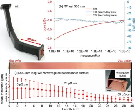
Cuoctane,Co/O3 process stands behind the CuDME,Co one because the latter is twice as fast and the cost of DME is typically 60% that of anhydrous octane. An additional advantage of the developed experimental protocols is that they exclude any release to air and thus prevent surface contamination and water uptake. The complete elucidation of the involved chemical and physical phenomena in the two protocols is out of the scope of this work and remains to be performed. We applied this knowhow to coat the interior surface of CFRP waveguides. To meet this objective, we reconsidered technical solutions of the DLI‐MOCVD process, such as the heating mode and the operating parameters, namely the gas flows and the operating pressure. We used the heated waveguide as the core of CVD reactor and subsequently adjusted the fluid flow through, and the thermal profile of the waveguide. Figure 4 resumes the obtained results. Photograph 4a shows a CFRP waveguide with a typical architecture, composed of metallized 60‐mm long straight sections, and of E‐plane and H‐ plane elbows that were assembled afterwards. This assembly demonstrates the ability of the developed processes to produce three‐dimensional functional waveguides. Such a coated straight CFRP section was successfully tested on a RF bench; however, the 60‐mm length sections are too short to provide robust conclusions. Therefore, in an attempt to get more reliable RF tests, we metallize straight, 300‐mm long WR75 CFRP waveguides. Diagram 4b shows the results of this RF bench test, namely the insertion loss and the standing wave ratio (SWR). SWR is less than ‐30 dB in the range 10 to 15 GHz, a value which meets the specifications; however, the insertion loss is 10 orders of magnitude above specifications. In order to identify the reasons of these high insertion losses, we sectioned the 300 mm waveguide into its four constitutive rectangles. The top part of Figure 4c presents a photograph of the bottom inner surface of the waveguide. Visual inspection of the coated CFRP surface reveals that the coating is patterned following the weaving of the composite material. The diagram below the photograph is the corresponding thickness of the film measured at 31 1‐cm equidistant points along the sectioned CFRP plate. The reported uncertainties for each point correspond to thickness variations along the width of the plate at a given length. It is recalled that the thickness was determined by X‐ray fluorescence and was verified in SEM cross‐sectional micrographs as the ones shown in Figure 2. We observe that the thickness varies between 5 ± 3 and 1.5 ± 1.5 μm, with a gradual decrease from the gas inlet to the gas outlet sides. Resistivity measurements reveal that it evolves in a similar way, from 18 μΩ.cm in the gas inlet side to 69 μΩ.cm at the gas outlet one. In addition, observation of both the rectangle plate and the entire waveguide prior sectioning reveals uncoated spots localized at the edges.
These observations illustrate non‐optimal control over both the Cu deposition process and the fabrication process of the CFRP waveguide. The latter should focus on the internal surface finishing prior metallization to ensure uniform chemical, energetic, and morphological characteristics. The deposition process requires dedicated design of the DLI‐MOCVD reactor because deposition on small samples occurs at local T, P, and flux conditions, whereas deposition in a long tubular part must take into account non‐uniform temperature and partial pressures fields along the longitudinal and lateral coordinates. In this perspective, multiscale and multiphysics computational modeling of the process based on an appropriately defined chemical kinetics mechanism will help to avoid resources waste in tremendous empirical experience plans. Corresponding simulations will serve as guide for targeting appropriate process parameters and technical
modifications such as interchanging gas inlet on both sides of the waveguide, rotating the waveguide, or implementing gas phase distribution entries. The combined improvement of both the surface finishing of the CFRP and of the deposition process is expected to provide Cu films with more homogeneous dimensional and functional characteristics that meet specifications. Comparable projects for coating the inner surfaces of 1‐m long nuclear cladding tubes by DLI‐MOCVD are already successful with such a combination of experiments and calculations [40].
Figure 4. Preliminary CFRP waveguide assembly made of 60‐mm long straight sections and both E‐plane and H‐plane elbows metallized with the CuDME,Co/untreated protocol (a). RF transport
results in terms of standing wave ratio (SWR) and insertion loss in the 10 to 15 GHz scale (b), photograph of the bottom inner surface (c, Top) and mapping of the thickness and electrical resistivity (c, Bottom) of a 300‐mm long WR75 waveguide metallized with the CuDME,Co/untreated
protocol.
4. Conclusions
Replacement of state of the art Al by CFRP radiofrequency waveguides in telecommunications satellites will result in strongly desirable mass reduction and superior thermal mechanical properties, provided an appropriate metallization process of the internal surface of the waveguides is developed. In the present contribution, we propose two innovative and scalable processes that meet this requirement. They both involve sequential direct liquid injection metalorganic chemical vapor deposition of copper and cobalt from (hfac)Cu(MHY) and Co2(CO)8, respectively. They result in almost
pure Cu films, with minor amount of Co localized at the interface with the CFRP. An ozone pretreatment of the polymer surface prior deposition, or the replacement of anhydrous octane by the cost effective anhydrous dimethoxyethane as solvent for the injection of the copper precursor, yield strongly adherent, 5 μm Cu films on the polymer composite. The activation energy of these process is almost half of the Cu deposition without Co2(CO)8, and deposition occurs at temperatures as low as 115 °C when DME is
used as solvent. In the latter case, we correlate the improved adhesion of Cu on the pristine polymer surface with the cleaning of the growing surface from detrimental to interfacial adhesion contaminants, coming from carbonyls and –CF3.
The electrical resistivity of the films is in the 4.1–5.0 μOhm∙cm range, and they sustain thermal cycling between −175 °C and +170 °C. The application of the DME involving protocol for the metallization of 60‐ and 300‐mm long CFRP waveguides resulted in a satisfactory −30 dB standing wave ratio but also in high values of insertion loss, attributed to non‐optimized deposition process and surface finishing of the CFRP. These results are state‐of‐the‐art for the development of a gas phase metallization process for CFRP waveguides. The reported positive evaluation of the DLI‐MOCVD process paves the way towards its qualification for the robust metallization of components at the meter scale. Author Contributions: The program was designed by C.V and T.D. after discussions with D.M. and Y.L. on the targeted specifications. F.A. performed experiments and analysis. T.D. and C.V analyzed the results and wrote the paper. Y.L. and D.M. analyzed the results, reviewed and edited the paper, and gave useful suggestions. All authors have read and agreed to the published version of the manuscript. Funding: The Conseil Régional Midi‐Pyrénées (contract no. 13052909) and the Agence Nationale de la Recherche (LabCom no. ANR‐14‐LAB3‐0010‐01) are acknowledged for financial support. Institutional Review Board Statement: Not applicable Informed Consent Statement: Not applicable Data Availability Statement: The raw data presented in this study are available on request from the corresponding author Acknowledgments: We are indebted to C. Josse (UMS Castaing, Toulouse, FR) for FIB preparations and SEM observations, and very grateful to Frederic Dumestre (Nanomeps, Toulouse, FR) for the preparation of the different precursor solutions and fruitful discussions. Conflicts of Interest: The authors declare no conflicts of interest. References 1. Beck, M. Composites: The Final Frontier. Compos. Manuf. 2014, 30, 14–17. 2. Reinhart, T.J. Engineered Materials Handbook: Composites; ASM International: Materials Park, OH, USA, 1987. 3. Anguita, J.V.; Smith, C.T.G.; Stute, T.; Funke, M.; Delkowski, M.; Silva, S.R.P. Dimensionally and environmentally ultra‐stable polymer composites reinforced with carbon fibres. Nat. Mater. 2020, 19, 317–322. 4. Alonso, F.; Fagoaga, I.; Oregui, P. Erosion protection of carbon epoxy composites by plasma‐sprayed coatings. Surf. Coat. Technol. 1991, 49, 482–488.
5. Lopera‐Valle, A.; McDonald, A., Application of flame‐sprayed coatings as heating elements for polymer‐based composite structures. J. Therm. Spray Technol. 2015, 24, 1289–1301.
6. Fallah, P.; Rajagopalan, S.; McDonald, A.; Yue, S. Development of hybrid metallic coatings on carbon fiber‐reinforced polymers (CFRPs) by cold spray deposition of copper‐assisted copper electroplating process. Surf. Coat. Technol. 2020, 400, 10.
7. Granado, L.; Kempa, S.; Gregoriades, L.J.; Bruning, F.; Bernhard, T.; Flaud, V.; Anglaret, E.; Frety, N. Improvements of the Epoxy‐Copper Adhesion for Microelectronic Applications. ACS Appl. Electron. Mater. 2019, 1, 1498–1505.
8. Zhang, J.H.; Zhou, T.; Wen, L. Selective Metallization Induced by Laser Activation: Fabricating Metallized Patterns on Polymer via Metal Oxide Composite. ACS Appl. Mater. Interfaces 2017, 9, 8996–9005.
9. Zhang, H.; Zhang, P.; Zhang, H.Z.; Li, X.H.; Lei, L.; Chen, L.N.; Zheng, Z.J.; Yu, Y. Universal Nature‐Inspired and Amine‐ Promoted Metallization for Flexible Electronics and Supercapacitors. ACS Appl. Mater. Interfaces 2018, 10, 28963–28970. 10. Xu, L.J.; Shi, X.Y.; Chai, M.Y.; Ji, J.; Xu, Z.K.; Wan, L.S. Surface Metallization of Porous Polymer Materials for Multifunctional
Applications. Langmuir 2020, 36, 1454–1461.
11. Yu, Y.; Yan, C.; Zheng, Z.J. Polymer‐Assisted Metal Deposition (PAMD): A Full‐Solution Strategy for Flexible, Stretchable, Compressible, and Wearable Metal Conductors. Adv. Mater. 2014, 26, 5508–5516.
12. Liu, J.S.; He, L.C.; Wang, L.; Man, Y.C.; Huang, L.Y.; Xu, Z.; Ge, D.; Li, J.M.; Liu, C.; Wang, L.D. Significant Enhancement of the Adhesion between Metal Films and Polymer Substrates by UV‐Ozone Surface Modification in Nanoscale. ACS Appl. Mater. Interfaces 2016, 8, 30576–30582.
13. Addou, F.; Duguet, T.; Bosso, P.; Zhang, A.N.; Amin‐Chalhoub, E.; Fanelli, F.; Vahlas, C. Metallization of carbon fiber reinforced polymers: Chemical kinetics, adhesion, and properties. Surf. Coat. Technol. 2016, 308, 62–69.
14. Boisselier, G.; Maury, F.; Schuster, F. SiC coatings grown by liquid injection chemical vapor deposition using single source metal‐organic precursors. Surf. Coat. Technol. 2013, 215, 152–160.
15. Czok, G.S.; Werther, J. Liquid spray vs. gaseous precursor injection—Its influence on the performance of particle coating by CVD in the fluidized bed. Powder Technol. 2006, 162, 100–110.
16. Joulaud, M.; Angekort, C.; Doppelt, P.; Mourier, T.; Mayer, D. Evaluation of (hfac)Cu(MHY) for CuCVD. Microelec. Eng. 2002, 64, 107–115. 17. Gooch, J.W. Encyclopedic Dictionary of Polymers. Springer: New York, NY, USA, 2011. 18. Duguet, T.; Senocq, F.; Laffont, L.; Vahlas, C. Metallization of polymer composites by metalorganic chemical vapor deposition of Cu: Surface functionalization driven films characteristics. Surf. Coat. Technol. 2013, 230, 254–259. 19. Ge, J.; Turunen, M.P.K.; Kivilahti, J.K. Surface modification and characterization of photodefinable epoxy/copper systems. Thin Solid Film. 2003, 440, 198–207. 20. Prysiazhnyi, V.; Stupavska, M.; Rahel, J.; Kleber, C.; Cernak, M.; Rafailovic, L.D. A comparison of chemical and atmospheric plasma assisted copper plating on carbon fiber reinforced epoxy polymer surfaces. Surf. Coat. Technol. 2014, 258, 1082–1089. 21. Schaubroeck, D.; De Baets, J.; Desmet, T.; Van Vlierberghe, S.; Schacht, E.; Van Calster, A. Introduction of amino groups on the surface of thin photo definable epoxy resin layers via chemical modification. Appl. Surf. Sci. 2009, 255, 8780–8787. 22. Yu, Z.J.; Kang, E.T.; Neoh, K.G. Electroless plating of copper on polyimide films modified by surface grafting of tertiary and quaternary amines polymers. Polymer 2002, 43, 4137–4146. 23. Ge, J.; Tuominen, R.; Kivilahti, J.K. Adhesion of electrolessly‐deposited copper to photosensitive epoxy. J. Adhes. Sci. Technol. 2001, 15, 1133–1143.
24. Siau, S.; Vervaet, A.; Schacht, E.; Van Calster, A. Influence of Chemical Pretreatment of Epoxy Polymers on the Adhesion Strength of Electrochemically Deposited Cu for Use in Electronic Interconnections. J. Electroch. Soc. 2004, 151, C133–C141. 25. Weiss, C.; Muenstedt, H. Surface modification of polyether ether ketone (peek) films for flexible printed circuit boards. J. Adhes. 2002, 78, 507–519. 26. Addou, F. Metallization of waveguides in epoxy matrix composite material by a DLI‐MOCVD process. Ph.D. Thesis, Institut National Polytechnique de Toulouse, Toulouse, France, 2017. 27. Allen, N.S.; Edge, M.; Mourelatou, D.; Wilkinson, A.; Liauw, C.M.; Parellada, M.D.; Barrio, J.A.; Quiteria, V.R.S. Influence of ozone on styrene‐ethylene‐butylene‐styrene (SEBS) copolymer. Polym. Degrad. Stab. 2003, 79, 297–307.
28. Gatenholm, P.; Ashida, T.; Hoffman, A.S. Hybrid biomaterials prepared by ozone‐induced polymerization. 1. Ozonation of microporous polypropylene. J. Polym. Sci. Part. A: Polym. Chem. 1997, 35, 1461–1467. 29. Siau, S.; Vervaet, A.; Nalines, S.; Schacht, E.; Van Calster, A. Kinetic study of wet chemical treatments on the surface roughness of epoxy polymer layers for buildup layers—I. Sweller influence. J. Electroch. Soc. 2004, 151, C816–C830. 30. Siau, S.; Vervaet, A.; Nalines, S.; Schacht, E.; Van Calster, A. Kinetic study of wet chemical treatments on the surface roughness of epoxy polymer layers for buildup layers—II. Oxidative treatment of the surface. J. Electroch. Soc. 2004, 151, C831–C849. 31. Siau, S.; Vervaet, A.; Van Vaeck, L.; Schacht, E.; Demeter, U.; Van Calster, A. Adhesion strength of the epoxy polymer/copper interface for use in microelectronics. J. Electroch. Soc. 2005, 152, C442–C455. 32. Amin‐Chalhoub, E.; Duguet, T.; Samélor, D.; Debieu, O.; Ungureanu, E.; Vahlas, C. Chemical vapor deposition of low reflective cobalt (II) oxide films. Appl. Surf. Sci. 2016, 360, 540–546.
33. Duguet, T.; Amin‐Chalhoub, E.; Samelor, D.; Pugliara, A.; Vahlas, C. Black Co oxides coatings for thermosensitive polymer surfaces by low‐temperature DLI‐MOCVD. Surf. Coat. Technol. 2018, 349, 941–948. 34. Li, Z.W.; Gordon, R.G.; Farmer, D.B.; Lin, Y.B.; Vlassak, J. Nucleation and adhesion of ALD copper on cobalt adhesion layers and tungsten nitride diffusion barriers. Electrochem. Sol. State Lett. 2005, 8, G182–G185. 35. Su, S.K.; Akiba, M.; Takahashi, T.; Saburi, M.; Hidai, M.; Uchida, Y. Chemical deposition in liquid‐phase (CDL)—A convenient method for cobalt‐coating or nickel‐coating of carbon fibers using zerovalent organometallic compounds. Chem. Lett. 1987, 16, 337–340. 36. Shimizu, H.; Sakoda, K.; Shimogaki, Y. CVD of cobalt‐tungsten alloy film as a novel copper diffusion barrier. Microelec. Eng. 2013, 106, 91–95. 37. Ye, D.X.; Pimanpang, S.; Jezewski, C.; Tang, F.; Senkevich, J.J.; Wang, G.C.; Lu, T.M. Low temperature chemical vapor deposition of Co thin films from Co2(CO)8. Thin Solid Film. 2005, 485, 95–100.
38. Eustathopoulos, N.; Nicholas, M.G.; Drevet, B. Wettability at High Temperatures; Pergamon Press: Oxford, UK, 1999; Volume 13, pp. 1–420. 39. Owens, D.K.; Wendt, R. Estimation of the surface free energy of polymers. J. Appl. Polym. Sci. 1969, 13, 1741–1747. 40. Michau, A.; Gazal, Y.; Addou, F.; Maury, F.; Duguet, T.; Boichot, R.; Pons, M.; Monsifrot, E.; Maskrot, H.; Schuster, F. Scale up of a DLI‐MOCVD process for the internal treatment of a batch of 16 nuclear fuel cladding segments with a CrCx protective coating. Surf. Coat. Technol. 2019, 375, 894–902.


![Figure 3. Arrhenius‐type plot showing the global metallization reaction kinetics in five different reaction systems. Data for the Cu octane reproduced from reference [13].](https://thumb-eu.123doks.com/thumbv2/123doknet/2938142.78827/9.918.276.532.653.1056/arrhenius-metallization-reaction-kinetics-different-reaction-reproduced-reference.webp)