HAL Id: tel-00943295
https://tel.archives-ouvertes.fr/tel-00943295
Submitted on 7 Feb 2014HAL is a multi-disciplinary open access archive for the deposit and dissemination of sci-entific research documents, whether they are pub-lished or not. The documents may come from teaching and research institutions in France or abroad, or from public or private research centers.
L’archive ouverte pluridisciplinaire HAL, est destinée au dépôt et à la diffusion de documents scientifiques de niveau recherche, publiés ou non, émanant des établissements d’enseignement et de recherche français ou étrangers, des laboratoires publics ou privés.
�Modeling and simulation of the IR-Drop phenomenon
in integrated circuits
Marina Aparicio Rodriguez
To cite this version:
Marina Aparicio Rodriguez. �Modeling and simulation of the IR-Drop phenomenon in integrated circuits. Electronics. Université Montpellier II - Sciences et Techniques du Languedoc, 2013. English. �tel-00943295�
Délivré par UNIVERSITE MONTPELLIER 2
Préparée au sein de l’école doctorale : Information, Structures, Systèmes (I2S)
Et de l’unité de recherche : Systèmes Automatiques et Microélectroniques (SYAM)
Spécialité : Microélectronique
Présentée par Marina Aparicio Rodriguez
Soutenue le 06/12/2013 devant le jury composé de
M. Michel RENOVELL, Directeur de Recherches,
CNRS, LIRMM, Université Montpellier II Directeur de thèse
Mme. Mariane COMTE, Maître de Conférences,
LIRMM, Université Montpellier II Co-encadrant de thèse
M. Laurent LATORRE, Professeur,
LIRMM, Université Montpellier II Examinateur
M. Joan FIGUERAS, Professeur,
Université Polytechnique de Catalogne Rapporteur
M. Jean-Michel PORTAL, Professeur,
Ecole Polytechnique Universitaire de Marseille Rapporteur
M. Ilia POLIAN, Professeur,
Université de Passau Examinateur
M. Bernd BECKER, Professeur,
Université Albert-Ludwings Examinateur
Mme. Florence AZAIS, Chargée de Recherches
CNRS, LIRMM, Université Montpellier II Invité
Modeling and simulation of the IR-Drop
phenomenon in integrated circuits
3
Abstract
Scaling technology in deep-submicron has reduced the voltage supply level and increased the number of transistors in the chip, increasing the power supply noise sensitivity of the ICs. Excessive power supply noise affects the timing performance, increasing the gate delay, and may cause timing faults. Specifically, power supply noise induced by the currents that flow through the resistive parasitic elements of the Power Distribution Network (PDN) is called IR-Drop.
This thesis deals with the modelling and simulation of logic circuits in the context of IR-drop. An original algorithm is proposed that allows to perform an event-driven delay simulation of the logic Block Under Test (BUT) while taking into account the whole chip IR-drop impact on the simulated block. To do so, we develop accurate and efficient electrical models for the currents generated by the switching gates, the propagation of the current draw through the PDN and the gate delays. First, the pre-characterization process for the dynamic currents, static currents and gate delays is described to generate a gate library. Then, another pre-characterization procedure is suggested to estimate the current distribution through the resistive PDN model. Our models are implemented in a first version of the simulator developed by the University of Passau in the context of collaboration. In addition, the impact of the parasitic capacitive elements of the PDN is analyzed and a procedure to derive the current distribution in a resistive-capacitive PDN model is proposed.
5
Résumé
L’évolution des technologies microélectroniques voire déca-nanoélectroniques conduit simultanément à des tensions d’alimentation toujours plus faibles et à des quantités de transistors toujours plus grandes. De ce fait, les courants d’alimentation augmentent sous une tension d’alimentation qui diminue, situation qui exacerbe la sensibilité des circuits intégrés au bruit d’alimentation. Un bruit d’alimentation excessif se traduit par une augmentation du retard des portes logiques pouvant finalement produire des fautes de retard. Un bruit d’alimentation provoqué par des courants circulant dans les résistances parasites du Réseau de Distribution d’Alimentation est communément référencé sous la dénomination d’IR-Drop.
Cette thèse s’intéresse à la modélisation et à la simulation de circuits logiques avec prise en compte du phénomène d’IR-Drop. Un algorithme original est tout d’abord proposé en vue d’une simulation de type ‘event-driven’ du bloc logique sous test, en tenant compte de l’impact de l’ensemble du circuit intégré sur l’IR-Drop du bloc considéré. Dans ce contexte, des modèles précis et efficaces sont développés pour les courants générés par les portes en commutation, pour la propagation de ces courants au travers du réseau de distribution et pour les retards des portes logiques. D’abord, une procédure de pré-caractérisation des courants dynamiques, statiques et des retards est décrite. Ensuite, une seconde procédure est proposée pour caractériser la propagation des courants au travers du réseau de distribution. Nos modèles ont été implantés dans une première version du simulateur développé par nos collègues de Passau dans le cadre d’une collaboration. Enfin, l’impact des éléments capacitifs parasites du réseau de distribution est analysé et une procédure pour caractériser la propagation des courants est envisagée.
7
Acknowledgements
!
It would not be possible to do this work without the help and kind support of people around me. To only some of whom it is possible to give particular mention here.
First of all, I would like to thanks my advisor, Dr. Michel Renovell, and my co-supervisor, Dr. Mariane Comte, for their patient guidance, encouragement and advices during these three years. I would like to express my gratitude for sharing their experience and supervising me in all steps of this work. It was a great pleasure to work with them.
I also appreciate working with Dr. Ilian Polian and Jie Jiang from the Department of Computing Engineering of the University of Passau. I would like to thanks them for this productive collaboration.
Finally, I would like to express my gratitude Dr. Joan Figueras, Dr. Jean-Michel Portal, Dr. Laurent Latorre, Dr. Florence Azais and Dr. Bernd Becker, for accepting to be members of the jury and coming to Montpellier (not without some unexpected problems).
Personally, I would like to thank my parents, Angel and Amparo, and my sister Paula. They have been there for me every step of the way, have always loved me unconditionally, and have aided me through all of my decisions.
Last but not the least, I would like to thank my partner, Thomas, who endured this long three years with me, supporting me in the worst moments and making rich the SNCF with so much travels. Without his support, patience and love, this adventure would not have been possible.
!
8
!
9
TABLE OF CONTENTS
Abstract ... 3 Résumé ... 5 Acknowledgements ... 7 TABLE OF CONTENTS ... 9 General introduction ... 11 1 Introduction ... 151.1 Context and state of the art ... 15
1.1.1 Power supply noise and IR-Drop definition ... 15
1.1.2 Power supply noise analysis ... 16
1.1.3 The design approach ... 18
1.1.4 The test approach ... 20
1.2 Objective and motivation ... 25
1.3 Algorithm principle ... 27
1.4 Physical vs electrical structure of the grid ... 32
2 Electrical model at gate level ... 35
2.1 Dynamic and static currents ... 35
2.2 Library models and variable parameters ... 40
2.3 Library pre-characterization ... 42
2.3.1 Delay model ... 44
2.3.2 Dynamic current model ... 49
2.3.3 Static current model ... 52
2.4 Pre-characterization constraints ... 56
10
3 Electrical model of the PDN current distribution ... 61
3.1 Electrical model for the current distribution in a resistive grid ... 62
3.1.1 PDN resistive model ... 62
3.1.2 The distribution factor ... 64
3.2 Electrical model for the current distribution in a resistive and capacitive grid ... 75
3.2.1 Different types of capacitive elements ... 76
3.2.2 Analysis of the capacitive elements ... 77
3.2.3 Theoretical analysis and simplified model ... 86
3.2.4 Electrical model for capacitive elements ... 93
4 Simulator implementation ... 97
4.1 Simulation principle and validation ... 98
4.1.1 Simulator algorithm ... 98
4.1.2 Simulation validation ... 102
4.1.3 Validation with a circuit designed to maximize the induced delay ... 108
4.2 Problematic of the simulation implementation using a RC grid ... 112
4.2.1 Capacitance window ... 113
4.2.2 Simplified model ... 117
4.2.3 RC model validation and conclusion ... 132
5 General conclusion and future work ... 139
Annex ... 143
TABLE OF FIGURES ... 149
LISTOFTABLES ... 153
REFERENCES ... 155
11
General introduction
Progress in deep submicron technology is focused on the increase of the transistor density in the chip and the increase of the circuit performances such as functional frequency. As a result, important power density problems due to the large amount of current required from the Power Distribution Network (PDN) have appeared, increasing the power supply noise. Excessive power supply noise can affect the circuit performances, causing problems such as signal integrity or additional delay. One of the main sources of power supply noise is the IR-Drop: an electrical phenomenon associated to the switching of logic gates. The inherent parasitic resistive elements of the PDN combined with the current drawn by the switching gates produce fluctuations in the supply voltage level. This work focuses on the supply voltage noise produced by the IR-Drop.
Design and optimization of the chip PDN is a very complex task because it is almost impossible to anticipate all the possible operational conditions of the chip. Nevertheless, designers try obviously to estimate the power supply noise and reduce as much as possible the IR-drop effects at the chip level. To do so, different supply network models have been proposed. Most of these works are based on vector-less approaches and primarily target the spatial impact of the IR-drop. Although design approaches obviate the vector dependence of the IR-Drop phenomenon, the statistical models allow to estimate the average power consumption at the chip level. This information is very useful to identify the critical areas and to consequently modify the PDN structure in order to minimize the undesirable voltage drop.
Concerning the test approach, the problematic is somehow different since the goal is to verify that the chip does not present any functional problem related to excessive delay due to IR-Drop. In this case, not only the spatial effect should be taken into account but also the temporal effect. Therefore power supply voltage analysis has to be addressed through a vector-dependent approach. However a vector-dependent approach is very time consuming and limited to the block level.
12
This document deals with the IR-Drop phenomenon from a test perspective, in particular, the modelling and simulation of logic blocks in presence of IR-Drop. The aim is to take into account the most relevant characteristics of the IR-Drop phenomenon in the block simulation:
• IR-Drop is a global phenomenon. The switching activity of a given block generates voltage drop impacting the whole chip. For this reason, voltage drop generated by the neighboring blocks must be taken into account during the block simulation.
• Voltage drop due to the IR-Drop dissipates in time and in space. Therefore, this works must develop accurate and efficient electrical models that allow a spatial and temporal simulation. • IR-Drop phenomenon comes from the logic switching activity. So IR-Drop requires a logic
vector-dependent simulation together with an electrical simulation to estimate the voltage drop in the PDN. Consequently, a mixed-mode simulation is necessary.
Therefore, an original algorithm is proposed allowing to perform an event-driven logic and timing simulation of the logic block under test while taking into account the whole chip IR-Drop impact on the simulated block. For the electrical simulation, accurate electrical models of the current draws and the gate delays are developed, as well as an electrical model that allows to compute the current distribution through the PDN. Our electrical models are implemented by the University of Passau in a first version of the simulator MIRID: Mixed-mode IR-Drop Induced Delay simulator. The development of the MIRID simulator is a joint project of LIRMM and the University of Passau funded by the German Research Council (DFG grant PO 1220/1-2) and by the BFHZ project FK 39-10.
This document is structured in four chapters followed by a general conclusion. In Chapter 1 an extensive description of the state of the art is presented, including the design and test approaches. The motivation of this work and the objective are also described in detail and then, the fundamental simulation principles are introduced.
In Chapter 2 the pre-characterization procedure to derive the gate library from SPICE simulations is explained. This library contains the electrical models for the parameters involved in an IR-Drop phenomenon at the gate level: dynamic currents, static currents and gate delays. All these elements are closely related to the technology and thus, a pre-characterization procedure is required for every technology. Other electrical parameters are taken into account to build the gate library: the input voltage swing, the supply voltage swing and the output capacitance. The used pre-characterization procedure to derive the electrical model from SPICE simulations for the dynamic current, static current and gate delay
13
for any electrical configuration is presented. Limitations of this pre-characterization process are also described.
Chapter 3 deals with the description of an electrical model for the PDN. This chapter is divided in two main sections: a first section where the PDN is modeled as a resistive grid and a second one where the capacitive elements present in the PDN are included in the resistive grid. For the resistive model, the current distribution through the grid is analyzed and a set of distribution factors is characterized. This set allows to estimate the current distribution through the resistive grid, taking into account the edge effect. Furthermore, a procedure to consider the impact of the neighboring blocks is proposed. In the second section, an extension of the electrical model of the PDN is presented. The impact of the capacitive elements in the current distribution through the PDN is analyzed and an electrical model is proposed for the three main capacitive elements present in the PDN: parasitic capacitors of the physical PDN, intentional decoupling capacitors and intrinsic decoupling capacitors due to non-switching gates.
Chapter 4 is also structured in two main sections. In the first one the simulation algorithm implemented in MIRID is described in detail. Then, signal waveforms and induced delays obtained from MIRID and SPICE simulations are compared in order to validate the gate library and the distribution factor principle. In the second section, we analyze the problem of implementing a PDN model with capacitive elements in the simulator. Mathematical computation of the current distribution is not possible due to the complexity and thus, a simplification method is described in order to estimate the current distribution. Although this method is not fully implemented in the simulator, preliminary simulations applying it are presented.
15
1 Introduction
1.1 Context and state of the art
1.1.1 Power supply noise and IR-Drop definition
Progress in deep submicron design is focused on the reduction of power consumption and the increase of the number of transistors in the devices. Simultaneously, technology scaling has continued to improve the performance of processors increasing the functional frequency. On the one hand, voltage scaling has reduced significantly the noise margin and, on the other hand, the ultra-high transistor density and rising frequency lead to a power density problem: a large amount of current is required, increasing the power supply noise [1]. As a result, excessive power supply noise can significantly affect the circuit performances and cause problems such as signal integrity [2] or additional delay [3]. Therefore, the increase of power supply noise has become a critical element in the performance and reliability of manufactured chips.
Power Supply Noise (PSN) refers to the voltage fluctuations in the power and ground distribution networks (PDN). The voltage fluctuations due to power supply noise in the PDN are generally called voltage drop. The power distribution network includes all the metal wires and vias that deliver power to every gate in the chip. This on-chip PDN is predominantly resistive but capacitive and inductive parasitic elements are also presented. Power supply noise is induced by current flows through the PDN:
• IR-Drop is generated due to the resistive elements of the PDN,
• ground bounce is generated due to the inductive elements of the PDN (!!.!" !"). This work focuses on power supply noise produced by IR-Drop.
16
IR-Drop is defined as an electrical phenomenon associated with the switching of MOS transistors. A current draw appears in the power supply connection and/or the ground supply connection when transistors switch. The inherent parasitic elements of the PDN combined with this current draw produce fluctuations in the voltage level. IC scaling technology has increased the density of transistors and the functional frequency. Thus, there are more gates switching simultaneously and consequently, voltage fluctuations have also increased due to the increase of the amount of current flowing through the PDN. As a consequence of these fluctuations, logic gates can be powered with a lower-than-normal Vdd or higher-than-normal Gnd or both, reducing the gate swing and impacting logic gates by an increased delay. Moreover the sensitivity of the gate delay to power supply noise increases with technology scaling. It has been reported that fluctuations of 10% in power/ground supply voltage increase gate delay by 8% in 180nm technology [4], but fluctuations of 10% can cause up to a 30% increase in gate delay in a 130nm technology [5], and a 1% change in power supply voltage causes nearly 4% of additional gate delay in 90nm technology [6]. The impact of power supply noise due to IR-Drop phenomenon has therefore become a critical concern, both for design and test aspects.
1.1.2 Power supply noise analysis
As the power supply noise becomes critical, analyzing its impact on the integrated circuit electrical behavior is today an important research topic. A good knowledge about the noise impact on the circuit functionality and timing performance can improve the design of the PDN and the test process.
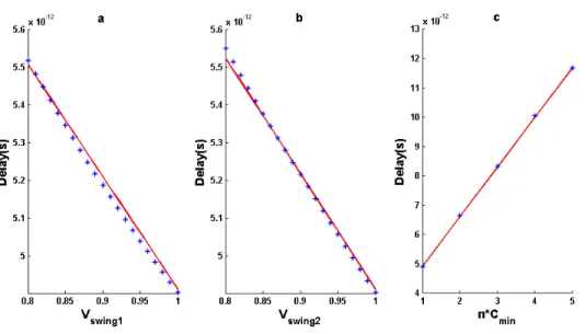
A voltage drop generated by a switching gate dissipates in time and space [7] as illustrated in Figure 1.1. Indeed, a current draw appears when the gate input switches and finishes after the commutation, when the output has become stable. It means that the voltage drop vanishes rapidly after the switching of the gate. On the other hand, current draw propagation is closely related to the PDN structure. The original current draw spreads through the PDN structure. Voltage drop due to the IR-Drop in a uniform power mesh spreads like a “bull’s eye” with “circular” equipotential rings [8]. Therefore, neighboring gates are more concerned by the voltage drop due to the IR-Drop phenomenon than gates locate far away from the original current draws. In brief, spatial and temporal analyses are necessary to describe the IR-Drop phenomenon.
17
Figure 1.1: A current draw injected into a power grid dissipates quickly in time (a) and space (b) [7].
Voltage variations in the power and ground supply networks have adverse impact on the delay of the gates connected to the supply networks and thus, timing faults can appear due to these variations. Consequently, analyzing the induced delay due to the power supply noise is becoming an important topic. The delay of a logic gate depends on many electrical factors such as supply voltage level, input voltage level, load capacitor, input slew rate and other electrical parameters of the gate [9]. Todri analyses the impact of power and ground supply noise in a path delay [10]. The conclusion is that power supply noise reduces the drive strength by changing the operational regions of the transistor, impacts the noise conditions on the neighboring gates by causing a speed-up or slow-down, and causes a delay shift due to the different voltage levels among the gates. Delay variations are further aggravated with package inductance, power/ground network parasitics, switching frequencies and technology scaling.
Regarding the electrical elements that have a significant impact on the power supply noise, we identify three important elements: the power distribution network, the current draw of the switching gate and the gate delay. The power distribution network and the package can be modeled as a combination of electrical elements. In [11] Panda proposes to use the following models for the package/on-chip power supply network:
• a RLC model for the package leads, ball grid arrays and power planes; • a RC model for the gate to power connections;
• a RC model for intrinsic decoupling capacitance of non-switching gates; • a RC model for intentional decoupling capacitances.
18
Regarding the electrical model at the gate level, most of the papers adopt a cell-based circuit model for the current draw and the delay in order to estimate the power supply noise. For some of these papers, an event-driven simulator uses the cell-library to inject a current draw into the PDN at the block level [12], [13], [14]. Other works estimate the global power supply noise based on a statistical approximation of the switching activity [15]. Finally other ones use the cell-library to consider the power noise information in a fault generator model [6].
For the gate delay, an analytical approach is used representing gate delay as a linear/quadratic function of the supply voltage in [9], [16]. Other publications propose a statistical approach to characterize delays [3]. Standard cell delay is treated as a perturbed random variable, and the probability functions are derived by simulating a set of characterization patterns.
For the current draw, most of the publications propose to model this current as a triangular function [3], [17] or as a trapezoidal function [2], [18]. These models adapt the shape of the current in function of the output capacitance and other electrical parameters. Some approximations are applied to simplify the electrical model. For example, the peak current is assumed to coincide with the transition at the gate input [17]. The value of the peak and the duration of the current are dependent on the gate type and the load capacitance.
Knowing the effect of the voltage supply noise, there are two traditional research directions:
• The first direction is to predict the power supply noise during the design phase and to manage it by design modifications.
• The second direction is to create test procedures to detect the timing faults generated by the power supply noise.
1.1.3 The design approach
The design of a good, reliable on-chip PDN of a digital IC is a very complex task because designers cannot anticipate all the functional conditions Design researches about the power supply sensibility try obviously to reduce as much as possible the whole power supply noise effect at the chip level. In essence, the principle is to estimate the supply voltage drop due to the IR-Drop and try to adapt the PDN design to minimize this phenomenon. To this aim, some techniques are applied during design to decrease the power supply noise and to improve the noise immunity of the circuits as explained by Larsson in [19].
The most widely used technique consists in adding decoupling capacitors between the power and ground supplies. Decoupling capacitors prevent the power noise from spreading through the PDN and
19
their inclusion in the design allows to isolate different areas on the chip. In this context most of the works try to develop algorithms to determine the optimal size and placement of the decoupling capacitors from the switching activities and the spatial correlations between different blocks. A power supply noise aware post-floorplanning methodology is proposed in [20], [21], [22]. Another research suggests to improve the traditional decoupling capacitor and to include active decoupling capacitors as a most effective technique to reduce the power supply noise [23].
Another classical way to reduce the power supply noise is to design a robust power distribution network. A lot of research works mark that traditional constraints in the PDN design are not enough to remove the IR-Drop timing faults. In order to improve the PDN design, most of the works propose a mathematical model to address the most important issues in the PDN design: width and pitch of PDN wires [8], [24], size, number and location of pads [25], [26], [27], [28], [29].Wire sizing for power and ground networks considering the IR-Drop induced by both the clocking and computing components is suggested in [24] and considering the IR-Drop and the area constrained in [8]. In order to determine the size, number and location of pads, [26] and [27] propose a closed form model for the power distribution network in N-metal layer system for wire-bond and flip-chip packages in function of given design constraints (as power dissipation, power supply voltage or static IR-Drop).
Other works focus on the correlation between different parameters of the on-chip power distribution grid and their impact on noise [25], [28], [29]. Results from this analysis can be used as guidelines when designing a robust power distribution network.
Models proposed by Rius [30] and by Shakeri [28], [29] exclusively focus on the IR-Drop phenomenon. Shakeri [29] demonstrates that the PDN can be approximated as a continuous layer of conductive material and that IR-Drop can be calculated by solving a system of partial differential equations, i.e. Poisson equation, with the proper boundary conditions. Shakeri [29] proposes a compact physical IR-Drop model of the on-chip power distribution grid and an IR-Drop model is derived for the wire-bond and the flip-chip packages. In this paper, the tradeoff between the package and the on-chip power distribution network parameters is studied in details. The size and number of pad tradeoff is also analyzed. The optimal placement of these pads is derived to minimize the IR-Drop. In brief, Shakeri suggests the use of a large number of small pads for the power distribution network instead of a small number of large pads to reduce the IR-Drop.
Based on the conclusion of Shakeri, Rius [30] suggests another IR-Drop model to determine the average power consumption of a block. Initially, the Drop is modeled in an infinite PDN. Then, the IR-Drop model in a finite PDN is derived from the infinite model solution. The suggested model provides an
20
accuracy estimation of the average power consumption of a block for the wire-bond package. Models of Shakeri and Rius help designers in the early stage of the design to estimate accurately the on-chip and package resources that need to be dedicated to power distribution, reducing the cost of over-design.
In brief, most of these works are based on a vector-less approach and primarily target the spatial effect of supply voltage noise. Suggested statistical circuit models estimate the average current consumption at the chip level, allow to identify the critical areas and to adapt the PDN network design in order to avoid the undesirable voltage drop. Although the design approaches do not take into account the input vector dependence of the IR-Drop phenomenon, the statistical models provide an estimated supply voltage drop at the chip level. We remember that a vector-based simulation at the chip level is non-viable due to prohibitive simulation costs.
Some commercial tools allow the optimization of the PDN. Apache has developed a full-chip power network analysis solution called RedHawk [31] that analyzes the effects of simultaneous switching noise (core, memory, I/O), decoupling capacitance (intentional and intrinsic), on-chip and off-chip package inductance. It provides a dynamical analysis of the power integrity based on a cell-based library and a less analysis of the switching activity. A mixed-mode between the less mode and a vector-based simulation of some blocks is included in the last versions of RedHawk. This assertion does not involve an event-driven simulation using vector patterns; it is an improvement in the statistical estimation of the switching activity at the block level.
RedHawk as the other commercial solutions, PrimeRail [32] from Synopsys and HyperLynx [33] from Mentor, provides a very accurate solution to optimize the PDN design and to place the decoupling capacitors. These solutions allow to minimize the voltage drop during the design stages but test stage is still necessary in order to detect timing faults due the power supply noise.
1.1.4 The test approach
As described in the previous section, design tools cannot completely guarantee a 100% IR-Drop free design; the chip may still manifest some IR-Drop originated functional problems. In this context, the test objective is twofold:
• Exacerbate the IR-Drop to detect the induced delay faults for non-scan test process • Minimize the IR-Drop to avoid over-kill for scan test process.
21
1.1.4.1 Maximum instantaneous current estimation
Early works propose to estimate the maximum instantaneous current in order to detect excessive switching activity in the IC and thus, reject these devices with a high risk of timing faults. Kriplani [17] estimates the maximum instantaneous current using a triangular function as the current draw model. In order to determine the maximum current, a vector-less algorithm called iMax is proposed. This algorithm computes all the possible commutations for every gate of the circuit and also all the possible associated waveforms. But it evaluates combinations of gate excitations that may not be possible. The maximum instantaneous current computed therefore is an upper bound of the worst case in a circuit. In addition, the suggested iMax algorithm is limited, it only estimates the maximum current for small blocks.
Jiang and Cheng [34] propose an improvement in the maximum instantaneous current estimation. Computation of the maximum instantaneous current is treated as an Integer Linear Programing (ILP) problem. ILP formulation allows to compute exactly the maximum instantaneous current for a small circuit using the gate library from [17]. For larger circuits, a partitioning-based approach is suggested. Large circuits are divided in sub-circuits whose maximum currents are computed independently. The maximum current of the circuit is the addition of all the maximum currents. In this case, the maximum current computed is again an upper bound of the real maximum current. The suggested ILP computation requires a longer CPU time in comparison with the iMax algorithm but the maximum instantaneous current estimated for small circuits is not overestimated.
In brief, the maximum instantaneous current estimated is the worst case for a circuit and it is overestimated. The maximum instantaneous current in a realistic operation mode would be much smaller and thus, test based on these methods can reject fault-free chips. In addition, a high current density does not necessary mean a delay fault, but just a risk.
1.1.4.2 Test pattern generation
In order to detect timing faults due to power supply noise some of the works propose to generate a small set of patterns to maximize the voltage drop noise. In this case, the test objective is to target the IR-Drop originated delay fault and to generate a delay test sequence able to exacerbate the IR-IR-Drop phenomenon.
Zhao [15] proposes to use Monte Carlo simulation and Genetic Algorithm in order to generate a set of patterns that induces the maximum switching noise. In this case, an event-driven simulation based on the correlation between switching events and a cell library is implemented. The cell library includes the delay and switching current in function of the input and output signal slopes and the output capacitance. The
22
switching noise is modeled as a weighted sum ofthe switching currents and the rates ofchange ofthese switching currents. The weights are respectively the effective resistance and inductance on the power and ground networks experienced by each switching current. The electrical model used to determine the effective resistance and inductance include a RL model for the packing and a RL model for the on-chip power distribution network. Finally, Monte Carlo simulation and Genetic Algorithm are used to search for the worst case input vector pair that induces the maximum switching noise.
Jiang and Cheng [13] also propose to generate small sets of patterns to maximize the voltage drop noise. In this case, the cell library is characterized in function of the power and ground pin characteristics and the power net RLC parameters as well as the starting voltage, ending voltage, and the slope of the input voltage. For the sake of simplicity, switching currents are modeled as a triangular function that depends on the input voltage variables. An event-driven logic simulation is developed in order to simulate a given input pattern. The power lines of the power distribution network are model as a RC tree. First, the effective waveforms in the power and ground lines for each small block (consisting of a set of adjacent cells) is computed. In order to propagate the waveform through the RC tree, look-up tables are generated in function of the electrical parameters of the power distribution network and the waveform of every cell. Later, the circuit is simulated for an input pattern applying the derived waveform. Based on this event-driven simulation for any given 2-vector sequence, a Genetic Algorithm is applied in order to generate a small set of patterns that would cause high power supply noise at a specified area.
Krstic [12], [14] improves the test pattern generation of Jiang and Cheng in order to sensitize the selected paths. The fitness value of the pattern is calculated as a summation of the maximum power supply noise for the nodes on the selected path. The Genetic Algorithm generates a set of pattern that maximizes the voltage supply noise in the nodes along the selected paths.
In summary, Zhao [15], Jiang and Cheng [13] developed event-driven simulators that allow to estimate the maximum power supply noise. However, both simulators compute the global power supply noise and do not take into account the impact of the power supply noise on the gate delays and on the switching currents. Although Jiang and Cheng [13] derive the waveform current in a RC tree, the estimation of the supply voltage noise through the on-chip power distribution network is not computed. Moreover, test pattern generated using these methods maximize the voltage supply noise and thus, present the same problem as the method based on the computation of the maximum instantaneous current.
23
Some other works tackle the pattern generation focusing on the type of voltage drop. Bhowmick [35] classifies the voltage drops into three broad categories following their locality in time and space:
• Low Frequency Power Drop (LFPD) affects the entire PDN after a few clock cycles
• High Frequency Power Drop (HFPD) in highly localized and is effective in the same clock cycle
• Mid Frequency Power Drop (MFPD) is localized in a small area but effective for more than a single clock cycle.
Polian [36] proposed a heuristic method to generate test sequences that create worst-case power drop by accumulating high and low frequency. To do so, Polian employs a dynamically constrained version of the classical D-algorithm to generate a sequence that maximizes the effects of both LFPD and HFPD. Bhowmick [35] addresses the problem of the multi-cycle droop faults due to the MFPD. A SAT-solver based ATPG for detection of these faults is developed for both combinational and full-scan circuits. Similarly to Polian, the resulting switching activity from the generated test vector may generate much higher power density and much higher IR-drop than in functional mode. In addition, both methods target the generation of switching activity without taking into account the electrical parameters at the gate level.
Another classical direction for IR-Drop testing is to try to adapt the test patterns to the realistic behavior of the tested circuits. It is known that power consumption during at-speed delay test can be different than during functional operation. Often a large number of transitions occur within a short time frame during the test operation in comparison with the normal circuit operation. In addition, test patterns can generate high switching activity in a small area of the circuit, increasing significantly the IR-Drop. It means that the test patterns applied in the test procedure generate an unrealistic IR-Drop and fault-free chip can be discarded. The objective of these works [37-44] is to adapt the test pattern generation for the at-speed delay test considering the IR-Drop.
Saxena [37] proposes to reduce the switching activity of the test patterns. This paper analyses the IR-Drop during at-speed test. Concretely, the toggling events are counted while a scan-based transition test is performed. Analyzing the toggle activity during a clock cycle, the study concludes that the toggle activity of certain pattern obtained from the ATPG is exacerbated in the first frames of the clock cycle. Saxena concludes that generation of patterns implying a more constant switching activity during a clock cycle reduces the peak of power consumption.
24
A method to generate patterns is proposed by Tehranipoor in a series of works [38], [39]. A statistical IR-drop analysis is performed to determine the blocks that consume more power and consequently endure a higher IR-Drop during the test pattern application. The probability of net toggle activity over the entire cycle period is derived from the statistical analysis. As most of the switching activity occurs during the early clock cycle period [37], the Switching Time Frame (STW) is identified as a more efficient unity of time than the clock cycle period. As the STW is variable in function of the test vector, the average switching time frame window is computed for every block. Consequently, the average switching power threshold for every block is estimated. On the other hand, a dynamic IR-Drop analysis is implemented and the average power consumption during the switching time frame (referred as switching cycle average power or SCAP) is calculated for every ATPG test pattern, rather than during a single tester cycle. Finally, test patterns with an associated SCAP over the average switching power threshold are discarded due to their exacerbated switching activity.
Other works address the distribution of switching on the chips. Certain test patterns generate hot-spots and consequently, high levels of IR-Drop appear in small areas of the chip. Lee [40] proposes a method to select test patterns from ATPG whose switching activity is distributed through the whole chip. The test pattern transitions are monitored: when a gate switches, the gate information and the load from the fan-outs are stored into the pattern transition profile set. In function of this information, Lee proposes to derive a Weighted Switching Activity matrix WSA from the complete profile sets for every test pattern. The WSA matrix represents the switching weights of a hypothetical single pattern during the launch-on-capture cycle. In addition, Lee derives the Maximum Weighted Switching Activity WSAmax. The WSAmax
matrix represents the maximum switching weights for a circuit independently of the test patterns. In order to reduce the number of test patterns, the test patterns are compacted such that the resulting WSA associated to the compacted test patterns do not exceed the switching threshold that is defined as a percentage of the highest maximum WSAmax. The paper concludes that fixing the switching threshold
around 20%, 25% and 30% of the maximum switching, the test coverage does not decrease significantly.
Other works use the ‘X-filling’ approach to reduce IR-drop effect during at-speed test. The X-filling method assigns 0's and 1's to unspecified ‘X’ bits in a test cube obtained from ATPG. This method reduces the circuit switching activity in capture mode and it is claimed that the X-filling method can be easily incorporated in the test flow because it requires only minimal changes in the existing ATPGs. In addition, the method does not affect the test data volume and the test time. Wen et al. propose a X-filling technique to reduce the IR-drop effect in a series of work [41], [42], [43]. In [41], only flip-flops transition activity is considered while in [42], both flip-flop and gate transition activities are studied. In [43], the authors focus on preventing the IR-Drop especially on gates that are close to the activated critical paths.
25
Other authors propose improvements in the X-filling method to reduce the IR-Drop during at-speed test: J. Li in [44] proposes to reduce both shift power and capture power during at-speed testing by improving the X-filling technique: i-filling method. In [45], spatial information is taken into account to reduce the IR-Drop effect during at-speed scan test. The IR-drop effect for each region is estimated using the WSA cost function.
In brief, the objective of these works is to minimize the IR-drop phenomenon while generating a test sequence during scan-test. In these works the used PDN model is very simplified and it is not representative of the whole chip IR-Drop impact.
1.1.4.3 Voltage drop fault models
Tirumurti [6] proposes a Generalized Fault Model (GFM) where power noise information is considered. A static timing analysis is performed instead of an expensive dynamic analysis. The waveform characterization is developed for every cell in function of the fanout and input signal slope. According to the layout, the suggested method classifies the cells as aggressor cells or victim cells. Obviously, power lines with a high number of aggressor cells will be more affected and so more sensitive to voltage drop. Areas affected by an important IR-Drop are detected using this procedure. Unfortunately, the worst voltage droop estimated by the fault simulator would never appear in functional mode because not all the aggressor cells will necessarily switch simultaneously during functional operation.
1.2 Objective and motivation
Regardless of maximizing or minimizing its impact, the IR-Drop phenomenon has become a critical point during the test phase and thus, IR-Drop induced delay has to be considered, predicted and evaluated in this phase. Direct dependence between switching activity, power noise and delay faults requires an accurate dependent simulation. Therefore, the objective of this work is to develop a vector-dependent IR-Drop timing-aware and logic simulation in order to be able to simulate test pattern sequences and to detect the appearance of delay faults. The challenge here comes from two strong limitations:
• Chip level. Classical fault oriented simulators (stuck-at faults, bridging faults…) are focused on the fault site and its propagation. In the case of IR-drop, there is no fault site, it is a global phenomenon generated by the chip as a whole. So to evaluate the IR-Drop impact, a global electrical model should be used together with an accurate vector-dependent simulation at the chip level. Obviously, it is not feasible. In the context of the PDN design optimization, developed models cannot be used for vector-dependent simulation due to prohibitive
26
simulation costs. In the test context, most of the works published in the literature use very simplified models of the PDN that permit to perform vector-dependent simulation. Of course, this is not representative of the whole chip IR-drop impact. Our objective is to propose a more refined model of the PDN that permits to take into account the whole chip IR-drop impact with a reasonable simulation cost.
• Block level. By definition IR-drop is an electrical phenomenon that implies currents flowing through resistances of the PDN. Consequently, IR-Drop generates supply voltage fluctuations that the electrical simulation at PDN level must evaluate. Electrical simulation using traditional electrical tools (SPICE-like simulation) is not feasible due to the prohibitive simulation cost and memory-constrained computation. The aim here is to develop an accurate and efficient model for the currents generated by the switching gates, the propagation of the currents through the PDN and the gate delays as a function of the voltage drop.
According to the above described simulation constraints, the simulation principles must be adapted taking into account the complexity of the electrical simulation of the PDN and the complexity of the logic simulation of the logic block. Therefore, the proposed electrical model must be a tradeoff between accuracy and a reasonable simulation time.
In this work, we propose a mixed-mode simulation including a logic and electrical simulation that allows to validate an input sequence of vectors at the block level. The voltage drop prediction will be a combination of the mixed logic-electrical simulation at the block level and the impact of the average consumption of the neighboring blocks. This means that the global impact of the IR-Drop is taken into account to increase the precision in the delay estimation.
However, electrical simulation at the block level is much time consuming and almost unfeasible. Consequently, the simulation principles must be optimized. One of the aims is therefore to propose an accurate electrical model that allows to perform a simplified electrical simulation without loss of accuracy in the gate delay prediction. The electrical model includes two main aspects, the gate level and the PDN level.
• Gate level. SPICE-like simulation of transistors is too complex and useless in our context. For our induced delay simulator not all electrical elements are concerned in the IR-Drop phenomenon and thus, these ones should be omitted. Roughly speaking, at the gate level there
27
are two parameters of interest: the gate current draw that flows through the PDN and the gate delay.
• PDN level: Supply voltage fluctuations may be predicted from the electrical elements of the PDN and the current flowing through these elements. Consequently, an accurate electrical model of the PDN including the most relevant elements, such as resistance, capacitance and inductance, must be proposed and more importantly, an efficient model to determine the current distribution inside the elements of the PDN needs to be defined.
Knowing that currents flowing through the PDN are a determinant point in the supply voltage prediction and thus also in the induced delay prediction, these currents can be classified in two general groups according to their time characteristics: dynamic and static currents. Dynamic currents correspond to the current draws generated when gates are switching. They flow from the PDN through the gate to the output capacitance or symmetrically, from the output capacitance to the PDN. Static currents are currents that flow across a logic gate while the gate inputs are stable and non-switching. It means that gates are consuming power permanently, but these currents are much smaller than dynamic currents. Both currents are extensively described in Chapter 2. Note that neighboring blocks also generate current activity. As justified previously, supply voltage noise is a global phenomenon at the chip level and so, the simulator must take into account the average current generated by the neighboring blocks (section 3.1.2.3). Although average current is a stochastic estimation, this estimation allows us to include the neighboring switching activity in our model without increasing the simulation cost.
1.3 Algorithm principle
An event-driven simulation algorithm is suggested to estimate the induced delays generated by the IR-Drop. As commented in the previous section, the IR-Drop algorithm principle is strongly dependent on a local-global duality on the one hand and on an electrical-logical duality on the other hand. The aim is to perform a logic vector-dependent block simulation at the block level that determines the logic and switching activity of the block and an electrical simulation of the PDN that estimates the supply voltage fluctuation.
Therefore, the general structure of the simulator is highly determined by this electrical-logical duality. The simulator is structured into two parts that correspond to the electrical level and the logical level:
• Electrical PDN model. The PDN model is a combination of resistors, capacitors and inductances representing the parasitic elements of the real PDN. In fact, the PDN is made of
28
two independent but completely similar PDNs: one for Vdd called Vdd PDN and one for Gnd called Gnd PDN. Complexity of the PDN model determines the precision in the supply voltage estimation and thus the accuracy of the delay estimation. For example, the model can be very simple as in the traditional delay induced simulators where PDN are not concerned in the delay estimation. For the first version of our simulator, the PDN is modeled as a resistive two dimensional grid (section 3.1). A more complex PDN model including capacitive elements is considered in Chapter 3 for a future version of the simulator.
• Logical block model. The logical model includes all logic gates of the block and their logic connections. The model also includes the connection of each gate to the Vdd PDN and Gnd PDN.
Therefore, the logic gates of the block being connected to the electrical PDN, every gate is assigned a node of the Vdd PDN and a node of the Gnd PDN. Figure 1.2 illustrates the general structure of the simulator and the connection between both models.
! Electrical) structure)of))the) Vdd)PDN)model)) Electrical) structure)of)the) Gnd)PDN)model)) Logical)structure) of)the)logic) block)model) Interconnected) electrical) components):)R,)C,)L…) Interconnected)logic)gates) <!#logic!gate,!#electrical!node>! Ni!! Ni!! Interconnected) electrical) components):)R,)C,)L…) <!#logic!gate,!#electrical!node>!
29
Figure 1.3 gives a functional view of the mixed-mode algorithm. A logic simulation is performed at the block level. Input patterns are applied to the block input generating the switching activity and propagating. Finally the output patterns and the estimated delay induced by the IR-Drop are obtained. Concurrently, in the electrical domain, the algorithm computes the current flows thought the electrical PDN model and estimates the supply voltage in every node of the PDN grid.
! Input& patterns& PDN&electrical&Simulation& Block&logical&simulation& Switching! Events! Output&patterns& +&Delay& Current& library&Vdd&& Delay&&&& library& Vdd&& Delay!! N(i,j)! N!(i,j)! Current& library&Gnd&& Switching! Events!+!delay! Gnd&& Switching! Events! IVdd!! Switching! Events! IVdd=>!VVdd!at!N(i,j)! IGnd=>!VGnd!at!N(i,j)! Supply! Voltage!! IGnd!!
Figure 1.3: Functional view of the simulation algorithm
Connection between the logic domain and the electrical domain is driven by the switching events. When a gate switches, the algorithm inserts in the event queue a switching input event. Then, for each event in the queue the electrical simulation:
• computes the supply voltage taking into account all the currents that are active in the PDN, • predicts the induced gate delay knowing the supply voltage,
• injects the corresponding current draw in the PDN model, • generates a switching output event with the predicted gate delay.
Gate current draws and delays are stored in an electrical library and depend on different parameters. Library pre-characterization process and parameters are extensively explained in Chapter 2.
30 ! ! Cload Vdd PDN model Logic block δ Gi ! ! ! ! ! ! ! ! ! ! ! ! ! ! ! ! ! ! ! ! ! ! ! ! Ngndi Nvddi ! t0 INgndi Gnd PDN model t ! t0 INvddi t Nvddi-1 Ngndi-1 t0 t0+δ Gi-1
Figure 1.4: Didactic view of the mixed-mode simulation
Figure 1.4 gives a didactic view of the simulation principle. Given a gate Gi connected to the PDN at
node Nvddi for the power supply and node Ngndi for the ground, when the gate input switches at time t0,
the simulation performs the following steps:
• Computation of the power supply voltage V!!""!!!(t0) using the electrical model of the Vdd
PDN.
• Computation of the power supply voltage V!!"#
!!!(t0) using the electrical model of the Gnd PDN.
31 !!"#$%& !! = !
!!""!!!!(!!)– !!!"#!!!(!!) 1.1
• Computation of the power supply voltage V!!""!(t0) using the electrical model of the Vdd
PDN.
• Computation of the power supply voltage V!!"#!(t0) using the electrical model of the Gnd
PDN.
• Computation of the voltage swing Vswing2 of the switching gate:
!!"#$%& !! = !
!!""!!(!!)– !!!"#!(!!) 1.2
• Libraryaccess to get the corresponding delay δ of the gate Gi as a function of Vswing1, Vswing2
and the load capacitance Cload:
! !! = ! !
!"#$%!(!!, !!"#$%!(!!), !!"#$%!(!!), !!"#$) 1.3
• Library access to get the corresponding current I!!""!(t0) in the power supply node Nvddi and
the current I!!"#
!(t0) in the ground supply node Ngndi as a function of Vswing1, Vswing2 and the load capacitance Cload:
!!!""!! = !! !!"#!""(!!, !!"#$%!(!!), !!"#$%!(!!), !!"#$) 1.4
!!!"#!! = ! !!"#!"#!(!!, !!"#$%!(!!), !!"#$%!(!!), !!"#$) 1.5
• Computation of the I!!""! and I!!"#! currents propagation into the Vdd PDN and Gnd PDN using the PDN electrical models.
32
1.4 Physical vs electrical structure of the grid
So far, the PDN has been presented as one of the most important elements to model accurately because currents flowing through the PDN and the resulting supply voltage fluctuations determine the gate delays and the potential delay faults. As it is well known, PDN is a complex system of wires delivering power to the whole integrated circuit through different layers. A PDN is classically organized as a set of parallel large wires located in the upper metal layers covering the whole circuit surface [30]. Obviously, the electrical PDN model depends on the physical structure of the PDN. For the sake of simplicity, we assume the following classical structure:
• In the top metal levels of the chip, high metal level #n and metal level #n-1 are exclusively composed of a set of parallel metal lines, these two sets having orthogonal directions. In the high metal levels through-vias that connect the two sets of orthogonal lines are regularly placed. The whole set of metal lines and through-vias creates a regular two-dimensional distribution network as represented in Figure 1.5.a. Usually, in a given level, one line over two is dedicated to Vdd and every other line to Gnd [36]; in this way, it is possible to analyze the Vdd distribution network and the Gnd distribution network as two independent three-dimensional distribution networks. Figure 1.5.a illustrates the two orthogonal networks for Vdd PDN and Gnd PDN.
• In the bottom metal levels of the chip, metal #2 is commonly used for the Vdd and Gnd lines. The Vdd and Gnd lines in the metal #2 level have typically a small length corresponding to the mega-cell they feed [36]. In addition they have multiple parallel via connections to the upper regular three-dimensional network as illustrated in Figure 1.5.c.
• Finally, intermediate metal level represents the interface between the upper regular three-dimensional network and the lower irregular structure as illustrated in Figure 1.5.b.
33 ! ! ! ! ! ! ! ! ! ! ! ! ! ! ! ! ! ! ! ! ! ! ! ! ! ! ! ! ! ! ! ! ! ! ! ! ! ! ! ! ! ! ! ! ! ! ! ! ! ! ! ! ! ! ! ! ! ! ! ! ! a) High Metal levels #8 #7 #6 …. Chip Spreading Regular/Regular b) Intermediate Metal level ex: #3 Chip Spreading Regular/Irregular c) Low Metal levels ex: #2 MegaCell Spreading Irregular 3-to-down Via 3-to-up Via Gate-to-power Via ! ! ! ! ! ! ! ! ! ! ! ! ! ! ! ! ! ! Metal #8 Metal #7 ! ! ! ! ! ! ! ! ! ! Metal #3 Metal #2 Gnd Gnd Gnd Vdd Vdd Vdd Vdd Gnd Gnd Figure 1.5: PDN topology
PDN topology is obviously optimized in the design phase to reduce the parasitic elements but they cannot be completely removed. And so, vertical crossings of conductive elements behave as capacitive elements and long wires and vias behave as resistive elements. In addition, inductive elements may be considered although these are very small and often neglected. Among all these parasitic elements, the resistive ones are really predominant; reason why IR-Drop is one of the most analyzed electrical phenomena due to the current flows through the PDN. Therefore, the distribution network model must contain an accurate representation and estimation of the PDN resistive elements.
In a modeling perspective, PDN topology can be divided into three areas:
• High metal level may be modeled as two independent two-dimensional resistive grids. The Vdd and Gnd lines in this level of the chip are very long, corresponding to the whole chip size. For this reason the parasitic resistances of the regular network are determinant in the current distribution through the PDN.
34
• Intermediate metal level may be considered as included in the two-dimensional grids.
• Low metal level is made of short metal connection (in the order of the mega-cell dimension) in comparison with the high metal level wires (in the order of the chip dimension). Moreover, there are multiple parallel via connections to the metal #3 lines that enable to reduce the resistive behavior of metal #2 lines. For these reasons, the parasitic resistance of this level can be neglected in the model.
In conclusion, the electrical model of the PDN concerns the two independent supply networks, which are physically regular, intertwined and orthogonal from one level to the other, and correspond to the high metal levels. We can accurately model the PDN as a symmetrical structure composed of two grids with resistive elements.
35
2 Electrical model at gate level
As introduced in the previous chapter, due to some current flows through the PDN, a supply voltage drop appears affecting the expected delays of the switching gates and so may generate timing faults. The current flows through the PDN can be created by logic gates that switch. Indeed, when a gate switches, a current is drawn from the voltage source to the gate through the PDN. This current generates a voltage drop in the PDN that affects the other gates. In other words, the voltage drop generated by a switching gate provokes a variation in the delay of the other gates. Therefore, a switching gate affects the gates that will switch later.
There are therefore two different electrical characteristics that need to be studied at this point: the current draw created by the switching logic gates and the impact of a supply voltage drop on the gate delay. Both elements, current draw and impacted delay, will be characterized in the gate library. Therefore, both the causes and the consequences of the IR-drop will be modeled in our gate library.
This chapter introduces the electrical parameters involved in the current flow and gate delay and gives a detailed view of the pre-characterization phase at the gate level.
2.1 Dynamic and static currents
As explained in Chapter 1, there are some intrinsic currents due to the electrical behavior of a logic gate. These intrinsic currents through the Vdd and Gnd power grids must be analyzed and modeled in order to implement our IR-Drop simulator. It is important to note that power consumption in ICs is a traditional research and classical topic in test researches and so we just reuse here the terminology and classification that is used in this field. Classically power dissipation is classified into two main groups: dynamic switching power dissipation and static power dissipation. According to this traditional classification, intrinsic currents can be divided into two general groups: dynamic and static currents.
36
Dynamic currents appear when the gate output terminal is switching. During the commutation time, the PMOS and NMOS devices of the gate progress through different operation regions, and the variation in the conductivity of the transistors generates different current flows. Analyzing the inverter as the simplest logic gate, there are two current flows through the inverter: the short current Ishort that flows from
Vdd to Gnd and the load current Iload that charges and discharges the output capacitance.
Figure 2.1 illustrates the inverter transfer curve and different operation regions, showing the output voltage in function of the input voltage, where VTN is the input voltage at which the NMOS transistor turns
from off to on (NMOS threshold voltage) and VTP is the PMOS threshold voltage (the PMOS transistor
turns from on to off region when the input voltage becomes higher than Vdd-|VTP|).
! NMOS%cutoff% PMOS%linear% Vi% Vo % NMOS%linear% PMOS%saturation% % NMOS%linear% PMOS%cutoff% % VTN% VDD%6%|VTP|% VDD% VDD% VOL% NMOS%saturation% PMOS%linear% % NMOS%saturation% PMOS%saturation% % Vo%=%Vi%6%|VTP|% Vo%=%Vi%6%VTN% VOH%
Figure 2.1: Inverter transfer curve
When analyzing for example an input transition from high to low level, the PMOS and NMOS transistors progress through the different operating regions during the transition: cutoff, linear and saturation. Based on the operating state of both transistors, five regions can be defined as illustrated in Figure 2.2 and in Table 2.1 (the transistors are considered ideal).
37 ! Region'1' PMOS!cutoff! NMOS!linear! Region'2' PMOS!saturation! NMOS!linear! ' time' Vi ' Region'3' PMOS!saturation! NMOS!saturation! ' Region'4' PMOS!linear! NMOS!saturation! ' Region'5' PMOS!linear! NMOS!cutoff! ' VTN' VDD'' VDD'3'|VTP|'
Figure 2.2: Transistor operating regions of an inverter (down transition)
Table 2.1: Regions of operation of transistors in a symmetrical CMOS inverter
Region Input voltage Vi Output voltage Vo NMOS transistor PMOS transistor
1 Vi ≥ (VDD - |VTP|) VOL = 0 Linear Cutoff
2 Vo + VTN < Vi ≤ (VDD - |VTP|) low Linear Saturation
3 Vi ≈ VDD/2 VDD/2 Saturation Saturation
4 VTN < Vi ≤ Vo + |VTP| high Saturation Linear
5 Vi ≤ VTN VOH = VDD Cutoff Linear
Region 1: When the inverter input corresponds to a logic 1, a high voltage (Vi≥ (VDD - |VTP|)) is
applied to the PMOS and NMOS devices. Then, the PMOS device is in the cutoff region and the NMOS device is in the linear region. There is no current Ishort flowing through the transistors from
Vdd to Gnd. In addition, the output voltage of the inverter being 0, there is no current flowing from the output capacitance to Gnd through the NMOS transistor.
Region 2: When the input signal starts to fall below the threshold voltage VTP of the PMOS transistor,
the PMOS device switches to the on mode and jumps into the saturation region. The NMOS device continues to be in the linear region. During this period, a current flow from Vdd to Gnd through the transistors, but this current is very small as the NMOS transistor behaves like a resistor in the linear region. A part of the current that flows across the PMOS transistor, Iload, charges the output
capacitance and the output voltage starts to rise.
Region 3: While the input voltage continues to decrease and for a very short slice of time, both devices are in the saturation region. For an ideal symmetrical inverter, both transistors are in the saturation region when the input voltage is Vdd/2. The current flowing through the PMOS device is at its maximum. Part of this current, Iload, charges the output capacitance and the rest, Ishort, flows through
38
Region 4: This region occurs when the input voltage is lower than (Vo+ |VTP|) but still higher than VTN. The PMOS device progresses into the linear region. The NMOS device continues in the saturation region and most of the current that flows across the PMOS transistor goes to charge the output capacitance (Iload). A small amount of the current flow goes from Vdd to Gnd (Ishort).
Region 5: Finally, the input voltage descends to logic 0. When the input voltage is below VTN, the
NMOS device turns off. The output voltage is stable and equal to the nominal Vdd supply voltage. Therefore the current flow through the inverter disappears.
It must be noted that the load current Iload flows from Vdd to the load capacitance crossing the PMOS
transistor as illustrated in Figure 2.3.a. For an input transition from low to high level, the load current Iload
flows from the load capacitance to Gnd the crossing the NMOS transistor as illustrated in Figure 2.3.b.
! Idyn% Cload% Cload% Iload% Ishort% a)%Falling%transition% b)%Rising%transition% Ishort% Iload% Idyn%
Figure 2.3: Dynamic currents in the inverter
In brief, the highest amount of dynamic current appears across the PMOS transistor in region 3, when both transistors are in the saturation region. Part of the dynamic current charges the output capacitance and the rest goes to ground across the NMOS transistor.
Concerning now the intrinsic static current, it appears even when the gate input does not switch. In past technologies, the magnitude of this static current was small and usually neglected. Technology scaling to reduce dynamic power requires the scaling of threshold voltage and oxide thickness, which results in an increase in static current. The intrinsic static current of a gate is traditionally called the quiescent current. This term is used to describe the amount of current consumed by a gate when the input edge does not change over time.
![Figure 1.1: A current draw injected into a power grid dissipates quickly in time (a) and space (b) [7]](https://thumb-eu.123doks.com/thumbv2/123doknet/7708189.246847/18.918.150.772.118.425/figure-current-draw-injected-power-dissipates-quickly-space.webp)