HAL Id: hal-02304842
https://hal.archives-ouvertes.fr/hal-02304842
Submitted on 7 Oct 2019HAL is a multi-disciplinary open access
archive for the deposit and dissemination of sci-entific research documents, whether they are pub-lished or not. The documents may come from teaching and research institutions in France or abroad, or from public or private research centers.
L’archive ouverte pluridisciplinaire HAL, est destinée au dépôt et à la diffusion de documents scientifiques de niveau recherche, publiés ou non, émanant des établissements d’enseignement et de recherche français ou étrangers, des laboratoires publics ou privés.
A novel approach of a fully inkjet printed SnO2-based
gas sensor on a flexible foil
Omar Kassem, Mohamed Saadaoui, Mathilde Rieu, Jean-Paul Viricelle
To cite this version:
Omar Kassem, Mohamed Saadaoui, Mathilde Rieu, Jean-Paul Viricelle. A novel approach of a fully inkjet printed SnO2-based gas sensor on a flexible foil. Journal of Materials Chemistry C, Royal Society of Chemistry, 2019, 7 (39), pp.12343 à 12353. �10.1039/C9TC04170B�. �hal-02304842�
A novel approach of a fully inkjet printed SnO
2-based gas sensor on a flexible foil
Omar Kassem a,b, Mohamed Saadaoui a, Mathilde Rieu b and Jean-Paul Viricelle b
a. Mines Saint-Etienne, Center of Microelectronics in Provence, Department of Flexible Electronics, France.
b. Mines Saint-Etienne, Univ Lyon, CNRS, UMR 5307 LGF, Centre SPIN, F - 42023 Saint-Etienne France
Abstract
In recent years, printed and flexible gas sensors have quickly emerged as an innovative area of great interest because of their lightness and low cost. These flexible sensors can be easily integrated into autonomous systems for many applications such as smart food packaging and premature disease detection. In this paper, a novel approach was applied to manufacture a fully inkjet-printed gas sensor on a flexible polymeric foil. Platinum heater and gold electrodes were printed on the top side of the substrate, separated by a thin insulating layer of printed polyimide. An aqueous sol-gel process was adopted to synthesize nanosized SnO2-based sol that guaranty a crystallization at 350 °C, which is
entirely consistent with the polyimide foil. Then, the sol was transformed into a stable ink and inkjet printed over the gold electrodes. The printability of different inks was optimized to ensure flawless ejection of droplets, and the complex physico-chemical interactions between the inks and different interfaces were controlled to get well-defined patterns with high resolution. Finally, electrical measurements of the printed sensor were performed to characterize the response and the sensitivity to different concentrations of ethanol, ammonia and carbon monoxide gases, at working temperature of 300 °C, in dry and wet air.
DOI: 10.1039/C9TC04170B
Introduction
The field of flexible and printed electronics is a burgeoning area in electronics development at academic and industrial level, because of potential applications in everyday life by printing electronic devices on large area soft substrates like plastic and paper [1]. Printing techniques offer wide advantages like rapidity, simplicity, eco-compatibility, and are the viable alternatives to the clean-room patterning processes like vacuum deposition subtractive technologies and lithography which involve multiple steps and high costs [2].
Among the different printing technologies, inkjet printing has gained a significant attention for its interesting characteristics. It is a digital and maskless patterning technique used to print well-defined patterns with less material wastage, on a wide range of substrates including textile, paper and plastic. Using inkjet printing, a picoliter volume of ink can be ejected in the form of droplets from the reservoir and through nozzles of a printhead. Nevertheless, challenges remain associated with the accurate control and stability of the jetting. Inkjet printing is a technology where several parameters interact, such as ink viscosity, surface tension, particles size and surface wettability [2]. Thus, it is essential to optimize inks compositions, printing parameters and annealing conditions for functional high resolution printed patterns.
A vast variety of materials can be deposited by inkjet printing, including metallic nanoparticles and nanowires [3–6], polymers [7,8], semiconductors [9,10], quantum dots [11] and carbon nanotubes [12]. These materials are used to produce different types of electronic components such as light-emitting diodes [13], biosensors [14,15], supercapacitors [16], transistors [17,18], and solar cells [19]. Recently, considerable attention has been given to inkjet printing of metal oxides based inks for gas sensing applications [20]. The fabrication of flexible gas sensors presents an interesting perspective for progress in many fields including premature medical diagnosis [21], detection of hazardous gases [22] and smart food packaging [23]. The commonly sensitive elements used for gas sensors are the semiconductor metal oxides like SnO2, ZnO, WO3, CuO, NiO, TiO2, CeO2 etc. [24–27]. They are low cost,
highly sensitive and have good thermal and structural stability. In addition, they are able to detect different type of environmental gases including oxidizing gases (NO2, O3) and reducing gases (ethanol, acetone, H2S, CO, NH3, CH4) [28,29]. However, crystallization of metal oxides requires annealing at high
temperature which can be problematic when polymers are used as a substrate.
Among the various types of metal oxides, tin dioxide (SnO2) is one of the most used material as an
active layer for gas sensor [30] because of its high sensitivity, chemical and structural stability, low cost, rapid response and its ability to detect many toxic and inflammable gases. SnO2 crystal structure
contains oxygen vacancies that make the material an oxygen-deficient n-type semiconductor. SnO2 is
synthesized in different forms (thin film, powder, nanowire, etc.) using various soft chemical synthesis methods, including polyol process [31], Okazaki method [32], chemical precipitation [33], organic-free synthesis method [34] and surfactant mediated method [35]. However, in comparison with other chemical synthesis processes, sol-gel is a simple and cost-effective technique, and appears to be very promising for deposition by inkjet printing. Wenfeng Shen [36] has formulate a SnO2-based ink by
alcoholic sol-gel process. The ink was printed on silicon and alumina substrates, and X-ray diffraction analysis shows that the rutile structure of SnO2 was obtained at an annealing temperature of 550 °C.
More recently, Rieu et al. [20] have successfully developed an alcoholic sol-gel method to prepare a SnO2-based ink, which was jetted on polyimide foil and annealed at 400 °C.
In our work, a new stable SnO2-based ink is formulated by aqueous sol-gel. The synthesized sol contains
highly dispersed nanocolloids smaller than 10 nm in size, which confers good stability to the ink and enable SnO2 to crystallize at a temperature below 400 °C, compatible with our flexible support.
Afterwards, inkjet printing technique is adopted as a deposition technology in order to fully print a flexible gas sensor based on tin oxide. The sensor is designed and printed in a novel multi-layer configuration to include all sensor elements on the top side of the plastic, in contrast to what is usually used where the heater is often integrated on the back-side of the substrate [20,22,37]. The sensor is made up of the following elements:
A platinum-based heater that activates the sensitive layer
Gold-based electrodes to connect the sensor to the electrical characterization bench A gas-sensitive layer based on SnO2
An insulating layer of polyimide that electrically insulates the platinum heater from the electrodes and the sensing SnO2 layer.
This original configuration leads to an easier integration of the sensor into an electronic data acquisition card. In addition, it reduces significantly the interface between the heater and the electrodes, which minimizes energy consumption.
We print platinum and polyimide inks that are newly commercialized and have never been reported, excepting a commercial gold ink which was reported in the literature [4,20]. We study the printability of these inks and perform the physical and electrical characterizations.
Finally, we present the sensor responses and sensitivity towards three gases: ethanol, ammonia and carbon monoxide, under dry and wet air, at 300 °C as operating temperature.
Experimental section
Inkjet printer specifications
For inkjet printing, we use a commercial lab-scale Dimatix inkjet-printer (DMP-2800, FujiFilm) equipped with a 10 pL cartridge. This printer requires an ink with surface tension in the range of 28 - 33 mN/m, viscosity in the range of 10 - 12 mPa.s, pH between 4 and 9, and particles size smaller than 200 nm to avoid nozzles clogging.
Formulation of SnO2-based ink by aqueous sol-gel process
SnO2-based sol was firstly prepared by aqueous sol-gel method as described in the literature for the
preparation of SnO2 nanopowders [38]. The synthesis method consists in dissolving tin chloride (SnCl2
99.99% - Sigma-Aldrich) in deionized water. Then, a 25% ammonia solution (NH4OH Sigma-Aldrich) was
added dropwise until the pH becomes slightly basic, for complete removal of chloride ions (Cl-).
Afterwards, tin hydroxide precipitate was recovered and dissolved in glacial acetic acid (CH3COOH 99% - Sigma-Aldrich) and ethylene glycol (EG, HO-CH2-CH2-OH 99.8% - Sigma-Aldrich) was added in order
to form a tin complex. The mixture was heated at 90 °C and a pale yellow sol containing a complex of tin cations was obtained after 1 h. In our previous work [39] an analysis carried out on the synthesized sol showed that the average diameter of the colloids was around 6 nm, and also confirmed the absence of aggregates in solution. Moreover, we successfully investigated the thermal behavior of the sol and
we found that a crystallized structure of SnO2, corresponding to a rutile structure, was obtained at 350
°C, which is entirely compatible with the use of polyimide foil.
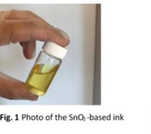
Synthesized sol was transformed into ink by evaporating the majority of the acetic acid to increase the ink pH up to 4 - 5, and by adding three solvents to adjust its rheology. For homogeneous and stable ink preparation, we used solvents with different boiling temperature (Tb) and vapor pressure (Pvap) as ethylene glycol (Tb = 197.3°C, Pvap = 8 Pa), glycerol (Tb = 290°C, Pvap = 0.4 Pa) and ethanol (Tb = 78°C, Pvap = 5800 Pa). Finally, 2-Isopropoxyethanol surfactant was used for fine-tuning of the surface tension [39]. The final SnO2 ink, shown in Figure 1, has a viscosity of 10 mPa.s and a surface tension of
32 mN/m, and exhibits a very good stability over time.
Designing and printing of gas sensor
A 50 µm thick polyimide foil was selected as a substrate (Upilex® S-Goodfellow). This plastic exhibits high thermal and chemical resistance and surface smoothness (Rz < 60 nm). Prior to processing, the substrate was cleaned by acetone, isopropanol and deionized water then it was dried in an oven at 120 °C for 30 minutes. Commercial gold (Au) ink (NPG-J from Harima, Japan) was used to print electrodes with an interspace of 300 µm. Platinum (Pt) ink, recently developed and marketed (Akko Lab LCC, Russia) was used to print the heating element. Electrodes and heater were printed on one side of Upilex foil and electrically separated each other by an insulating layer of polyimide which is printed using a commercial and high thermal resistance polyimide (PI) ink (PI 6643-001 JNC corporation, Japan). Finally, SnO2 ink prepared by sol-gel process was deposited onto the polyimide
and over gold electrodes. The shape of the sensing element was a square of 1 mm2. Rheological
properties of commercial inks provided by suppliers and SnO2 ink prepared in our previous work are
summarized in Table 1, and the multilayer configuration used to manufacture a fully inkjet flexible gas sensor is shown in Figure 2.
Table 1 Properties of commercial inks at 20 °C
Pt ink Akko Lab, LCC Au ink NPG-J PI ink PI 6643-001 SnO2 ink Kassem et al. [39] Viscosity [mPa.s] 15 – 25 7 20 10 Surface tension [mN/m] 30 – 40 25 30 32 Solid cotenant [% wt.] 5 53 30 5 Particles size [nm] 6 7 - 6
Solvents Ethylene glycol Petroleum
hydrocarbon γ-Butyrolactone Diethyleneglycol ethylmethyl ether Ethylene glycol Ethanol Glycerol 2isopropoxyethano l
Optical microscopy, Scanning Electron Microscopy (SEM), and Atomic Force Microscopy (AFM). Morphology of printed patterns was firstly observed by binocular microscope (Nikon SMZ1500) and optical microscope (Nikon Eclipse LV150). Observations of platinum film at nano-scale were performed using a Zeiss Ultra 55 SEM equipped with an energy dispersive spectroscopy (EDS), and by AFM Nanowizard III (JPK Instruments AG, Germany) in the tapping mode. The AFM image was obtained from a 1 µm2 surface, scanning with 512 by 512 pixels. A cross-section lamella of all printed layers was
prepared using Focus Ion Beam (FIB) (Equipex MANUTECH-USD). Carbon and platinum were deposited on the top of the sample during the preparation of the lamella. Thickness of printed layers was determined by SEM.
Surface energy measurement. Surface energy and contact angle measurements were characterized using a goniometer (Apollo Instrument OCA200, Dataphysics). We use Owens–Wendt–Rabel–Kaelble (OWRK) method to calculate the surface energy of the substrate [39].
Characterization of electric resistivity of printed metal thin films. Kelvin structures were used to characterize the electrical resistivity of printed Au and Pt thin films. The resistance (R) was measured using a 4-point probe system (SÜSS MicroTec PM5) with a Keithley 2010 source-meter. The electrical resistivity was calculated using the following formula:
ρ (Ω. m) = R(Ω). S(m2) L (m)
Where L is length of the printed patterns measured by optical microscope (Nikon Eclipse LV150) and S is the section determined by mechanical profilometer (Ambios XP-2), taking into account the effect of material accumulation at the edges, known as the "Coffee-ring".
Electro-thermal simulation and calibration of the heater. Comsol Multiphysics 5.3 software was used to optimize the design of the heater using electro-thermal simulation. Platinum and polyimide properties presented in table 2 were used. Then, the temperature coefficient of resistance (α) of Pt printed and sintered at 350 °C was characterized experimentally using the Kelvin structure described above. The experiment was performed in a clean room 1000 with controlled temperature and humidity conditions. The sample placed on a Peltier thermoelectric module (European Thermodynamics, Ref: GM250-127-14-16) was polarized under 4 points to accurately measure its electrical resistance at different temperatures. A thermometer based on fiber optic gallium arsenide (AsGa) with an accuracy
of ± 1 °C was used to determine the temperature (Optocon, Fotemp1). The temperature coefficient of resistance (α) was extracted from a linear regression of the following formula:
R(T) = R0(1 + α∆T) Where R0 is the resistance at room temperature (T0) and ΔT = T – T0
Table 2 Properties of polyimide and platinum
Properties Polyimide [40] Platinum [41]
Heat capacity [J/kg.K] 1130 133
Thermal conductivity [W/m.K] 0,29 71
Density [kg/m3] 1300 21450
Electrical resistivity [µΩ.cm] n.a. 35. (1 + 0,0029. ∆𝑇)
Thickness 50 µm for Upilex, and 4 µm for printed polyimide 130 nm
Electrical characterizations of the sensor. Electrical characterizations of the fully-printed sensor were performed using three different gases: Ethanol (C2H5OH), ammonia (NH3) and carbon monoxide (CO),
in dry and wet synthetic air. The sensor was installed in an 80 cm3 glass chamber under constant gas
flow of 10 L.h-1. Cylinders of Ethanol (555 ppm, diluted in nitrogen), NH
3 (297 ppm diluted in nitrogen)
and CO (300 ppm diluted in air) purchased from Air Product and Chemicals Company were used. Before injecting the target gas in the test chamber, the sensor was kept for one night at operating temperature to desorb organic species and to achieve good conductance stability. By applying a supply voltage, the platinum heater printed under the SnO2 sensitive layer enabled to heat up the sensor between 100
and 300 °C. Gas injections were done using gas flow meters controlled through LabView software. Conductance measurements were performed by electronic unit equipped with voltage divider circuit, and data acquisition was done with LabView software also. After stabilization of the sensor at 300 °C under dry air, a thermogram showing the evolution of the sensor conductance during a slow temperature descent to 100 °C, with a ramp of 1°C/min, was recorded. The conductance of the sensor was then stabilized under 20 ppm ethanol for 1 h at 300 °C, then the variation of the conductance under C2H5OH as a function of temperature was studied between 300 °C and 100 °C with the same
1°C/min ramp. The samples undergo the same thermal cycle with the same conductivity measurements under 20 ppm CO and 20 ppm NH3.
In the next step, sensor response measurements, 20 min exposure to gas/air mixture and 30 min recovery in air, were recorded for different gas concentrations. We define relative response of the sensor as: (G-G0)/G0
Where G0 is the initial conductance of SnO2 measured under air just before injection of target gas, and
G is the conductance after 20 minutes of gas injection. Relative response was plotted versus gas concentrations to monitor the sensor response and to calculate its sensitivity. Sensor sensitivity is a characteristic parameter. It expresses how large is the change in the sensor signal upon a certain change in gas concentration, in other words, it is defined as the slope of the relative response curve versus target gas concentrations.
Results and discussion
Sensor design
The sensor was designed and printed in multilayer configuration to embed all the elements of the sensor on the plastic top face. The process steps are illustrated in Fig. 3.
Following the cleaning and drying of the substrate, a single layer of polyimide was printed on Upilex foil (Fig. 3a). This step was integrated into the fabrication process owing to the difficulties faced when Pt ink was printed directly on Upilex, and it will be discussed later in this paper. Then, Pt ink was printed on polyimide layer to prepare the heating structure (Fig. 3b). Next, a second polyimide layer was printed over the first one and on platinum layer simultaneously (Fig. 3c). This new polyimide layer provides electrical insulation between the heater and electrodes that were printed on the second polyimide layer using Au ink (Fig. 3d). Finally, a sensitive layer based on SnO2 was deposited over the
gold electrodes (Fig. 3e). This configuration enables the sensor to be easily interfaced with the electrical characterization test bench of the sensor or in electronic acquisition card. In addition, the thickness of the printed polyimide is 10 times lower than that of Upilex substrate given at 50 µm. Therefore, the integration of the heater and the sensitive layer on the top surface of the plastic foil will
reduce the interface between these two elements, which can limit heat dissipation and consequently minimize the energy consumption of the sensor.
Preparation of an electrical insulating layer of polyimide by inkjet
PI 6643-001 polyimide ink has a surface tension of 30 mN/m and a viscosity of 20 mPa.s at room temperature (Table 1). Printing an ink with such high viscosity requires high nozzles temperature and high excitation voltage to compensate for the increase in elongational viscosity during ejection [42]. Raising up nozzles temperature decreases the fluid viscosity, but a large increase in nozzles temperature can destabilize the ink by promoting solvents evaporation, which causes clogging nozzles [43]. Therefore, it is essential to find a good compromise of nozzles temperature to facilitate the ink ejection without clogging the nozzles. A value of 32 °C was retained in this case. In addition, a waveform adapted to the rheological behavior of the polymer ink also had to be defined as depicted in Fig. 4.
The waveform has two main phases that essentially influence the piezoelectric element deformation and the droplet ejection. The first phase setting allows defining the amount of ink that will be drawn from the reservoir to the micro-chamber. Phase 2 setting is performed to define the quantity and speed of ink ejection via the nozzles. These two consecutive phases can be adjusted in terms of “slew rate” and “duration”, which indicate how fast the piezoelectric element is deformed and how long it remains in this position, respectively.
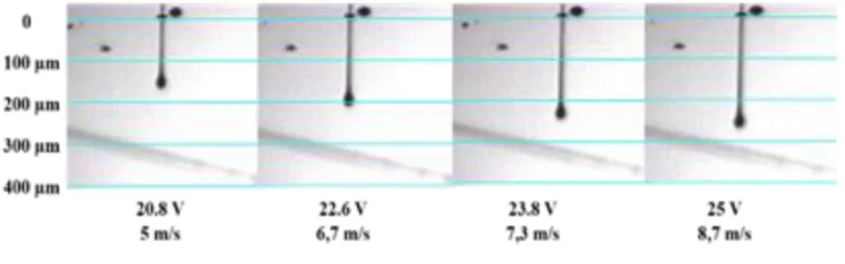
In the case of polyimide printing, adjustments were made on phase 2 while observing individual jet with the built-in drop watcher camera of the Dimatix printer. In comparison with the standard waveform [39] the duration was extended from 4 to 14 µs and the slew rate was increased from 0.9 to 1.3 V/µs. This optimization step aims to prevent the ink deceleration caused by the ink wettability on the nozzle during the ejection phase and to overcome the viscoelastic behavior of the ink that opposes its detachment from the nozzles. Afterwards, ejected droplets were observed as function of the voltage applied on piezoelectric membrane, called “firing voltage”. We found that the application of firing voltage between 20 and 25 V is the best compromise that ensure the formation of a stable jet. For lower ejection voltages, the drop may not be easily ejected, while the application of very high excitation voltage may result in the formation of satellites droplet, because the surface tension of the fluid can not sustain the fluid in one droplet. Therefore, a main droplet is separated from the tailing part which forms satellites [44].
Fig. 5 shows sequential images of drop formation, 30 μsec after ejection, at different firing voltage values between 20 and 25 V, captured with stroboscopic flashes. The imposition of an increasing electrical potential on the piezoelectric membrane results in a higher drop ejection rate, leading to a straight ejections with longer ligament behind the spherical portion of the drop. This behavior is characteristic of the inkjet printing of a low molecular weight viscoelastic polymer [45].
In parallel to the firing voltage adjustment, the drop spacing has to be optimized to ensure a good surface coverage when printing a continuous polyimide film on Upilex foil. The surface energy value of Upilex measured was 47 mN/m. Polyimide droplets were first printed at different operating voltages and their diameters are measured using an optical microscope. Fig. 6 shows the obtained results. Uniform spherical droplets were observed, which confirms the compatibility of the polyimide ink surface tension (30 mN/m) with the Upilex surface energy (47 mN/m). The increase in firing voltage increases the velocity and the printed volume, resulting in larger diameter droplets [6]. An average width of 72 ± 1.4 μm, obtained for an applied firing voltage of 20.8 V, increases to 86.8 ± 1 μm for a firing voltage of 25 V. Therefore, the drop spacing was set at 30 - 35 µm, depending on the selected voltage, to achieve the overlap of the deposited drops necessary for a homogeneous and continuous film.
Then, a square-shaped polyimide layer was inkjet printed on Upilex foil and heated at 80 °C for 5 minutes and then at 350 °C for 30 minutes for solvents evaporations and complete imidization of polyimide precursor, according to the ink supplier. The surface energy measurement of the polyimide printed film by OWRK method gave a value of 40 mN/m. This value is higher than the surface tension
of PI ink (30 mN/m), Au ink (25 mN/m), Pt ink (30 - 40 mN/m) and SnO2 ink (32 mN/m) (Table 1) and
will ensure good inks spreading without the need for a surface treatment.
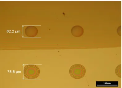
In the proposed fabrication process, the polyimide ink (PI - 6643-001) must be printed on a polyimide layer pre-printed and polymerized on Upilex (Fig. 3c). Therefore, a drop test was carried out partly on the polyimide film to determine the optimal drop spacing to get a continuous layer. Using an average value of the firing voltage (23 V), single droplets of polyimide ink deposited on the pre-printed polyimide film have a mean diameter of 62 ± 1 μm, and are smaller than the droplets deposited on Upilex foil using the same firing voltage (diameter ≈ 78 ± 1 μm, Fig. S1 ESI†). This is due to the surface energy of printed polyimide film (40 mN/m) which is lower than that of Upilex (47 mN/m), resulting in a lower spread of the deposited droplets. The drop spacing of printed polyimide ink was set at 30 μm in this case.
Inkjet printing of Au ink
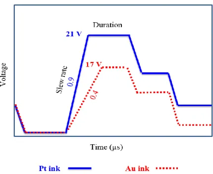
Au and Pt metal inks have very different rheological properties, which necessitates specific optimizations of the ejection conditions for each ink. In comparison with PI and Pt inks, Au ink exhibits low viscosity and surface tension values (Table 1), which requires less time to form the drop. Thus, a controlled printing of Au ink was achieved by applying a low firing voltage of 17 ± 1 V and by decreasing the slew rate of the waveform ejection phase to around 0.4 V/µs (Fig. S2, ESI†). Furthermore, nozzles temperature was set at ambient temperature and a 5 inch H2O vacuum was applied, to prevent the ink
from flowing by gravity through the cartridge nozzles.
Now the ink ejection conditions are optimized, it is possible to proceed to the evaluation of the printed patterns quality. The Au ink surface tension given by the supplier at 25 mN/m is much lower than the surface energy of both Upilex foil (47 mN/m) and printed polyimide layer (40 mN/m), which leads to a significant spreading of the ink once it is deposited on the substrate. To overcome this problem, the drop spacing was set to 45 µm and the platen temperature was maintained at 50 °C to promote the ink solvents evaporation and consequently the spreading of the ink would be reduced [46,47]. Once the gold ink was printed, the resulting film was sintered at 200 °C for 1 h to evaporate solvents and organic residues and to coalesce the gold nanoparticles on which it is possible to print the SnO2 sensitive layer. In order to characterize Au layer, a final annealing step was performed at 350 °C for 2 h. This temperature was dictated by the crystallization temperature of SnO2 (Fig. 3e). Annealing steps were carried out in standard oven using a ramp of 5 °C/min. The electrical resistivity of Au printed pattern annealed at 350 °C (2 h) was 13 µΩ.cm, which is 5 times higher than the resistivity of bulk gold (ρ = 2.44 µΩ.cm at 25 °C).
Preparation of platinum heater by inkjet Inkjet printing of Pt ink
Pt ink present a relatively high viscosity (15 - 25 mPa.s). Thus, drop ejection was optimized by increasing the nozzles temperature to 30 °C to decrease the viscosity using the standard waveform provided by the printer and a firing voltage of 21 ± 1 V (Fig. S2, ESI†). In addition, Pt ink contains low weight percentage (5% wt.) of metal nanoparticles. It is therefore essential to print multiple layers to reduce the electrical resistance of the resulting film. In our case, we printed 4 layers of Pt by heating up the printer platen at 40 °C during the printing process to ensure fast evaporation of solvents and limit the loss in resolution of the printed pattern.
The final annealing of Pt patterns was dictated by the cumulative annealing temperature of the polyimide ink, gold and SnO2 inks which was done at 350 °C for 3 h. Our first results show that thin
films of platinum ink, printed directly on Upilex and sintered at 350 °C were not electrically conductive. An elemental analysis by EDS reveals a discontinuity in the platinum film (Fig. S3, ESI†). We assumed that this phenomenon could be attributed to the viscoelastic mechanical deformation of Upilex foil, characterized by a high out-of-plane thermal expansion coefficient (αz from 100 ppm/°C to 400 ppm/°C between 20 °C and 400 °C) compared to the in-plane one (from 5 ppm/°C to 10 ppm/°C) and the manifestation of the glass transition temperature around 300 °C [48,49]. Thus, the thin platinum layer is mixed with a polymer from Upilex substrate when the annealing temperature exceeds 300 °C as confirmed by the increase of the carbon peak in the EDS spectrum, thus leading to local electrical and morphological discontinuity.
However, printing platinum on the pre-printed polyimide layer, and annealing it at 350 °C for 3 h results in the formation of a conductive film (Fig. S4, ESI†), and confirms that the high electrical resistance observed at 350 °C is directly related to the use of Upilex as a substrate and not to platinum ink. The difference in surface roughness and surface energy between the two polyimide (substrate and layer) can influence on Pt deposition, but we assumed that the main reason for Pt film discontinuity is the high thermal expansion of Upilex substrate and its viscoelastic deformation. This problem was overcome by the introduction of an intermediate polyimide layer that may also act as a buffer. Observation of the platinum film printed on polyimide by SEM and AFM (Fig. S5, ESI†) shows a compact microstructure with significant coalescence where the particles size was estimated at 30 - 40 nm, compared to the initial size of the Pt nanoparticles of about 6 nm (table 1). We therefore used the printed polyimide as an interface between Upilex and the rest of the gas sensor layers.
Calibration of printed platinum heater
To establish the correlation between electrical resistivity, printed lines widths and annealing conditions, 3 Kelvin structures of platinum with a length of 700 µm, and widths of 100 µm, 200 µm and 300 µm were printed and sintered at several combinations of sintering temperature and time, as shown in Fig. 7. It can be observed firstly that for a fixed temperature, it is possible to achieve low resistivity values by heating for a longer period. The sintering time has a significant influence on the film resistivity, but when temperatures above 150 °C were applied, this influence becomes less important on the final resistivity. The lowest resistivity values are those obtained after annealing the samples at 350 °C for 3 h.
Moreover, we notice that the bars associated with the resistivity of structures with line widths of 200 µm (red) and 300 µm (blue) are almost the same height, indicating that the resistivity is similar under different annealing conditions and thus, the annealing mechanism is similar for both structures. On the other hand, the resistivity bar of the structure with a 100 µm wide (green) shows higher overall resistivity values, which can be associated with the coffee-ring effect promoted by heating the printer platen up to 40 °C during printing, encountered more easily when small width structures are printed by inkjet [50]. Therefore, a line width of 200 µm was chosen to design and manufacture the heater because of its small dimension, and its consistent resistivity values, in the same order of magnitude as those obtained with the 300 µm line.
A platinum-based heater was prepared by inkjet and used to rise the temperature around the sensitive area made by SnO2. The variation of the resistance versus temperature is given in Fig. 8 and a linear
fitting of the resulting curve is used to extract the temperature coefficient (α) of printed platinum.
The obtained coefficient is 0.0029°C-1 which is lower than the one of the bulk platinum given at
0.0039°C-1. This difference can be attributed to several parameters: the nanometric size of platinum
particles [51], the substrate nature [51] and the complex microstructure of the metallic thin film which will bring more barriers during the electron-transfer process [52].
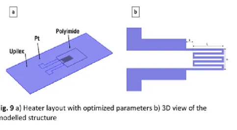
Electro-thermal simulation of heater
In order to obtain both a homogeneous temperature distribution on a surface corresponding to that of the SnO2 layer (1 mm²) together with a low power consumption, heater simulation was developed
thanks to Comsol software. The heater structure including Upilex, platinum and printed polyimide was modeled in 3D (Fig. 9a) considering thermal and electrical properties of these materials (Table 2). A serpentine structure has been studied with geometrical parameters (a, L, n, described in Fig. 9b) that are going to be optimized. In this study, printed polyimide was considered to have the same characteristics as Upilex, because the thermal properties of the printed polyimide are unknown. The thickness of the Pt film found at 130 nm (Table 2) was extracted from the section of printed Pt pattern using a mechanical profilometer (Ambios - XP2), taking into account the important coffee-ring effect of the printed pattern (Fig. S6, ESI†). The "free triangular" mesh type was used with a maximum element size of 100 µm (Fig. S7, ESI†). Simulations were subsequently carried out to study the influence
of the number of fingers (n) and their length (L) on the temperature distribution and the power output. Distance “a” has been set at 900 µm and the width of the interconnection between heating resistor and pads was extended at 1300 µm to limit heat diffusion to the external connections. The track width and inter-line heater spacing were set at 200 µm and 160 µm, respectively.
Fig. 10 shows the dependence of maximum temperature and electrical power on geometric dimensions. To reach a temperature of 300 °C, the power output must be between 360 and 400 mW. This power range can be obtained by optimizing the couple (n, L). Therefore, the number of resistance fingers was set at 3 (corresponding to a total width of 2480 µm) and their lengths at 4.3 mm to minimize the total size of the heater while promoting a uniform temperature distribution over a millimetric surface as shown in Fig. 11.
To compare the simulation results with the experiment, a heater with n = 3 and L = 4.3 mm was manufactured by inkjet printing and annealing at 350 °C for 3 h. Electrical voltages between 4 and 12 V were applied to determine the resistance and the corresponding electrical power. The temperature was deduced using the temperature coefficient (α) of platinum at 0.0029 °C-1. The obtained results
show a very good agreement between the thermal response experimentally achieved and the simulation (Fig. 12). At 300 °C, the error percentage between the applied and simulated electrical power was about 3.5 %. The power output (360 – 400 mW) can be reduced by printing more Pt layers to decrease the initial electric resistance, or by reducing the active surface area, to get a miniaturization of the structure and a gain on the applied power.
Gas sensing characterizations
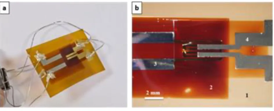
After the optimization of the printing and annealing conditions of polyimide, platinum and gold inks, the preparation of a fully inkjet printed gas sensor was carried out using the process explained in the Fig. 3. Two transparent layers of SnO2 (1 mm2) were printed over the electrodes by introducing an
intermediate annealing step at 350 °C between each printing step to avoid cracks formation in the printed film [39]. The sensor is illustrated in Fig. 13. SEM cross-sectional images presented in Fig. 14 show that the thicknesses of the Pt, PI, Au and SnO2 printed films were around 55 nm, 4 µm, 180 nm
and 100 nm, respectively.
A study was performed to determine the temperature at which SnO2 sensor exhibits a maximum
response to 3 different gases: ethanol, ammonia and carbon monoxide (Fig. 15). The results show that SnO2 conductance in dry air increases with temperature until it reaches a maximum between 150 °C
and 200 °C. This is a classic behavior observed in SnO2-based sensors studies [53]. In addition, the
conductance of SnO2 under ethanol shows a continuous increase until 300 °C.
Fig. 15 shows that the maximum response of SnO2 under NH3 is also increasing up to 300 °C. In addition,
a particular phenomenon was observed in the case of ammonia detection. Indeed, we notice that at temperatures below 225 °C, the conductance of SnO2 exposed to NH3 was lower than the one obtained
under dry air. This phenomenon has been reported previously by Kamalpreet Khun et al. [54] and by Hijazi et al. [26]. They explained this phenomenon by different reaction mechanisms at low and high temperatures. Consequently, NH3 has a reducing behavior at temperatures above around 225 °C, and
Finally, the maximum conductance of SnO2 under CO was at 250 °C, but the difference between
conductance under dry air and conductance under CO was slightly higher at 300 °C. Thus, in the next experiments, sensors temperature will be fixed at 300 °C.
Fig. 16 shows the response of SnO2 flexible sensor at 300 °C, upon exposure to different concentrations
of C2H5OH, NH3 and CO (from 5 to 100 ppm under dry air and from 10 to 100 ppm under wet air). The
sensor was swept under dry air for 1 night at 300 °C to stabilize its electrical conductance. First, it can be seen from Fig. 16 that the conductance of SnO2 increases when exposed to the target gas and it
drops rapidly and returns its original state when the injection was stopped in the testing chamber in each cycle, indicating that the SnO2 gas sensor has reversible response for different C2H5OH, NH3 and
CO concentrations under dry air. These gases exhibit a reducing character. They react with the ionosorbed oxygen species and release electrons to the conduction band according to equation (1), which leads to an increase of conductance [55]. Test bench configuration did not allow estimating any response time due to significant dead volume.
R + O- → RO + e- (1)
In order to evaluate the sensor sensitivity under dry air, the relative response (G-G0) / G0 was plotted
as a function of the gases concentration injected into the cell. Fig. 16 shows that the relative response increases with increasing gases concentration, and the sensor is quite sensitive in low range [0 – 20 ppm] but rapid signal saturation occurs for higher gases concentrations. Indeed, the sensor exposed to ethanol exhibit a sensitivity around 1.36 ± 0.17 ppm-1 between 0 and 20 ppm. After this
concentration, the sensitivity starts to decrease and reach approximately 0.25 ± 0.1 ppm-1 between 40
and 100 ppm. The same phenomenon was observed when the sensor was exposed to ammonia and to carbon monoxide under dry air. For NH3, the sensitivity of the sensor was 0.14 ± 0.03 ppm-1 between
0 and 20 ppm and it decreased to 0.005 ± 0.001 ppm-1 for higher concentrations. Finally, the sensitivity
[40 – 100 ppm] when the sensor was exposed to CO gas under dry air. We notice that the fully inkjet sensor is able to detect gases at low concentrations, which is very interesting, especially for environmental and medical applications. For instance, the lower limit of human ammonia perception by smell is close to 50 ppm. However, even below this limit, ammonia causes serious problems to the health like irritation of the respiratory system, skin and eyes [56]. Moreover, measuring ammonia levels in exhaled air can be a fast diagnostic method for patients with Helicobacter pylori bacterial stomach infection [57].
Environmental humidity is an important factor that influences the performance of metal oxide gas sensors. We tested the effect of moisture on the conductance and response of fully inkjet printed SnO2
sensor. The water vapor behaves like a reducing gas and causes an increase in the conductivity of the sensor [58]. The effect of humidity was studied on the conductance and response of the sensor when exposed to different concentrations between 10 and 100 ppm of C2H5OH, NH3 and CO, as shown in Fig.
16. Although the sensor responses to the 3 gases under wet air are low compared to the responses found under dry air, these responses remain reversible and dependent on the concentrations of the injected gas. It should also be noted that sensors tested under wet air are less sensitive than those tested under dry air. Indeed, the adsorption of water on the surface of SnO2 causes an increase in the
conductance baseline of the sensor and thus leads to a decrease in response and sensitivity. In addition, the competitive adsorption of water molecules leads to a decrease in the chemisorption of oxygen species on the SnO2 surface due to the decrease in the active sites responsible for gas sensing
phenomena [59].
Like other metal oxides, SnO2 sensors exhibit lack of selectivity. In order to improve the selectivity, two
strategies are considered:
The first involves a surface functionalization of the SnO2 sensitive layer using an organic
functional groups having different polarities, which leads to a change of the sensor response toward specific gases like ammonia [26].
The second implies the incorporation or the doping of atoms into the SnO2 structure [60]. This
method is consistent with the inkjet printing as it can be done during the sol preparation by sol-gel method.
Conclusion
In summary, a flexible SnO2 gas sensor was successfully deviced using inkjet printing technology. SnO2
-based sol was synthetized by aqueous sol-gel method, and then transformed into ink with suitable rheological properties. SnO2 could be crystallized at 350 °C, which is entirely consistent with the use of
polyimide substrate. Platinum was chosen as the base material for the sensor heater. Platinum printing was optimized and Kelvin structures were printed on the polyimide to perform electrical calibrations for the heater simulation and design. Platinum heater and gold electrodes were printed on the top side of Upilex substrate, separated by an insulating layer of printed polyimide. Then, 2 layers of SnO2
were printed over the gold electrodes and annealed at 350 °C for 1 h. The proper operation of the prepared gas sensor was validated under exposure to different concentrations of C2H5OH, NH3 and CO
gases, under dry and wet air, at 300 °C.
References
1 S. Katsuaki, Introduction to Printed Electronics, Springer New York, 2014. 2 N. C. Raut and K. Al-Shamery, J. Mater. Chem. C, 2018, 1618–1641.
3 E. Balliu, H. Andersson, M. Engholm, T. Öhlund, H.-E. Nilsson and H. Olin, Scientific Reports. 4 Y. Khan, F. J. Pavinatto, M. C. Lin, A. Liao, S. L. Swisher, K. Mann, V. Subramanian, M. M. Maharbiz and A. C. Arias, Advanced Functional Materials, 2016, 26, 1004–1013.
6 W.-D. Chen, Y.-H. Lin, C.-P. Chang, Y. Sung, Y.-M. Liu and M.-D. Ger, Surface and Coatings Technology, 2011, 205, 4750–4756.
7 F. Zhang, C. Tuck, R. Hague, Y. He, E. Saleh, Y. Li, C. Sturgess and R. Wildman, Journal of Applied Polymer Science, 2016, 133, n/a-n/a.
8 A. De Girolamo Del Mauro, R. Diana, I. A. Grimaldi, F. Loffredo, P. Morvillo, F. Villani and C. Minarini, Polymer Composites, 2013, 34, 1493–1499.
9 S. Sharma, S. S. Pande and P. Swaminathan, RSC Advances, 2017, 7, 39411–39419.
10 C. Costa, C. Pinheiro, I. Henriques and C. A. T. Laia, ACS Applied Materials & Interfaces, 2012, 4, 1330–1340.
11 V. Wood, M. J. Panzer, J. Chen, M. S. Bradley, J. E. Halpert, M. G. Bawendi and V. Bulović, Advanced Materials, 2009, 21, 2151–2155.
12 S. Kholghi Eshkalak, A. Chinnappan, W. A. D. M. Jayathilaka, M. Khatibzadeh, E. Kowsari and S. Ramakrishna, Applied Materials Today, 2017, 9, 372–386.
13 Z. Xing, J. Zhuang, C. Wei, D. Zhang, Z. Xie, X. Xu, S. Ji, J. Tang, W. Su and Z. Cui, ACS Applied Materials & Interfaces, 2017, 9, 16351–16359.
14 E. Bihar, T. Roberts, M. Saadaoui, T. Hervé, J. B. De Graaf and G. G. Malliaras, Advanced Healthcare Materials, 2017, 6, 1601167.
15 J. Li, F. Rossignol and J. Macdonald, Lab on a Chip, 2015, 15, 2538–2558. 16 P. Chen, H. Chen, J. Qiu and C. Zhou, Nano Research, 2010, 3, 594–603.
17 P. M. Grubb, H. Subbaraman, S. Park, D. Akinwande and R. T. Chen, Scientific Reports.
18 K. Y. Mitra, M. Polomoshnov, C. Martínez-Domingo, D. Mitra, E. Ramon and R. R. Baumann, Advanced Electronic Materials, 2017, 3, 1700275.
19 S. G. Hashmi, M. Özkan, J. Halme, S. M. Zakeeruddin, J. Paltakari, M. Grätzel and P. D. Lund, Energy & Environmental Science, 2016, 9, 2453–2462.
20 M. Rieu, M. Camara, G. Tournier, J.-P. Viricelle, C. Pijolat, N. F. de Rooij and D. Briand, Sensors and Actuators B: Chemical, 2016, 236, 1091–1097.
21 H.-Y. Li, C.-S. Lee, D. H. Kim and J.-H. Lee, ACS Applied Materials & Interfaces, 2018, 10, 27858– 27867.
22 M. Acuautla, S. Bernardini, L. Gallais, T. Fiorido, L. Patout and M. Bendahan, Sensors and Actuators B: Chemical, 2014, 203, 602–611.
23 S. Matindoust, M. Baghaei-Nejad, M. H. Shahrokh Abadi, Z. Zou and L.-R. Zheng, Sensor Review, 2016, 36, 169–183.
24 E. Kanazawa, G. Sakai, K. Shimanoe, Y. Kanmura, Y. Teraoka, N. Miura and N. Yamazoe, Sensors and Actuators B: Chemical, 2001, 77, 72–77.
25 L. Zhu and W. Zeng, Sensors and Actuators A: Physical, 2017, 267, 242–261.
26 M. Hijazi, M. Rieu, V. Stambouli, G. Tournier, J.-P. Viricelle and C. Pijolat, Sensors and Actuators B: Chemical, 2018, 256, 440–447.
27 A. Dey, Materials Science and Engineering: B, 2018, 229, 206–217. 28 G. Sberveglieri, Sensors and Actuators B: Chemical, 1995, 23, 103–109.
29 K. Wetchakun, T. Samerjai, N. Tamaekong, C. Liewhiran, C. Siriwong, V. Kruefu, A. Wisitsoraat, A. Tuantranont and S. Phanichphant, Sensors and Actuators B: Chemical, 2011, 160, 580–591.
30 H.-J. Kim and J.-H. Lee, Sensors and Actuators B: Chemical, 2014, 192, 607–627.
31 Y. Wang, X. Jiang and Y. Xia, Journal of the American Chemical Society, 2003, 125, 16176– 16177.
32 M. Honoré, S. Lenaerts, J. Desmet, G. Huyberechts and J. Roggen, Sensors and Actuators B: Chemical, 1994, 19, 621–624.
33 C. Fu, J. Wang, M. Yang, X. Su, J. Xu and B. Jiang, Journal of Non-Crystalline Solids, 2011, 357, 1172–1176.
34 A. Zarkov, A. Stanulis, L. Mikoliunaite, A. N. Salak and A. Kareiva, Thin Solid Films, 2018, 649, 219–224.
35 Y. Wang, C. Ma, X. Sun and H. Li, Nanotechnology, 2002, 13, 565–569. 36 W. Shen, Sensors and Actuators B: Chemical, 2012, 166–167, 110–116.
37 I. D. P. Hermida, G. Wiranto, Hiskia and R. Nopriyanti, Journal of Physics: Conference Series, 2016, 776, 012061.
38 H. Köse, Ş. Karaal, A. O. Aydin and H. Akbulut, Materials Science in Semiconductor Processing, 2015, 38, 404–412.
39 O. Kassem, M. Saadaoui, M. Rieu, S. Sao-Joao and J. P. Viricelle, Journal of Materials Science, 2018, 53, 12750–12761.
40 Upilex - Ultra heat-resistant films (Grade details) | UBE Heat-resistant Polyimide Materials, http://www.upilex.jp/en/upilex_grade.html.
41 David R. Lide, CRC Handbook of Chemistry and Physics, 84th Edition.
42 R. I. Haque, R. Vié, M. Germainy, L. Valbin, P. Benaben and X. Boddaert, Flexible and Printed Electronics, 2016, 1, 015001.
43 Y. He, R. D. Wildman, C. J. Tuck, S. D. R. Christie and S. Edmondson, Scientific Reports. 44 M.-H. Tsai and W.-S. Hwang, MATERIALS TRANSACTIONS, 2008, 49, 331–338.
45 Z. Du, X. Yu and Y. Han, Chinese Chemical Letters, 2018, 29, 399–404.
46 C. Gaspar, T. Sikanen, S. Franssila and V. Jokinen, Biomicrofluidics, 2016, 10, 064120.
47 T. H. J. van Osch, J. Perelaer, A. W. M. de Laat and U. S. Schubert, Advanced Materials, 2008, 20, 343–345.
48 S. T. Chen and H. H. Wagner, Journal of Electronic Materials, 1993, 22, 797–799.
49 S. Heltzel, C. O. A. Semprimoschnig and M. R. J. Van Eesbeek, High Performance Polymers, 2008, 20, 492–511.
50 C.-F. Liu, Y. Lin, W.-Y. Lai and W. Huang, AIP Advances, 2017, 7, 115008.
51 J. Zhang, Y. Nagao, S. Kuwano and Y. Ito, Japanese Journal of Applied Physics, 1997, 36, 834– 839.
52 Y. Tao, Y. Tao, B. Wang, L. Wang and Y. Tai, Nanoscale Research Letters, , DOI:10.1186/1556-276X-8-296.
53 G. Tournier and C. Pijolat, Sensors and Actuators B: Chemical, 2005, 106, 553–562. 54 K. Khun Khun, A. Mahajan and R. K. Bedi, Journal of Applied Physics, 2009, 106, 124509. 55 M. E. Franke, T. J. Koplin and U. Simon, Small, 2006, 2, 36–50.
56 B. Timmer, W. Olthuis and A. van den Berg, Sensors and Actuators B: Chemical, 2005, 107, 666– 677.
57 D. J. Kearney, T. Hubbard and D. Putnam, Dig Dis Sci, 47, 2523–2530. 58 N. Yamazoe, J. Fuchigami and M. Kishikawa, 10.
59 C. Wang, L. Yin, L. Zhang, D. Xiang and R. Gao, Sensors, 2010, 10, 2088–2106. 60 X. Guan, Y. Wang, P. Luo, Y. Yu, D. Chen and X. Li, Nanomaterials, 2019, 9, 445.
Supporting Information ESI†
Figure S1. Optical microscopic view of polyimide ink single droplets deposited on polyimide film (top)
Figure S2. Jetting waveform of Dimatix Inkjet-printer adapted for platinum and gold inks
Figure S3. a) SEM image and the corresponding EDS spectra of the platinum layer printed on Upilex
Figure S4. Image observed by binocular microscopy onto 2 different substrates: Upilex (left) and
printed polyimide (right) and annealed at 350 °C
Figure S5. Morphology of the platinum film printed on the polyimide and annealed at 350 °C,
Figure S6. Section of platinum pattern measured by mechanical profilometer