affiliée à l’Université de Montréal
Circuit
s techniques for wireless sensing systems in
high-temperature environments
AHMAD HASSAN
Département de génie électrique
Thèse présentée en vue de l’obtention du diplôme de Philosophiae Doctor Génie électrique
Avril 2019
affiliée à l’Université de Montréal
Cette thèse intitulée:
Circuit
s techniques for wireless sensing systems in
high-temperature environments
présentée par Ahmad HASSAN
en vue de l’obtention du diplôme de Philosophiae Doctor a été dûment acceptée par le jury d’examen constitué de :
Yves AUDET, président
Mohamad SAWAN, membre et directeur de recherche Yvon SAVARIA, membre et codirecteur de recherche François LEDUC-PRIMEAU, membre
DEDICATION
To my beloved parents To my dear wife To my daughter and son To my sister and brothers To my dear friends.
ACKNOWLEDGEMENTS
I would like to express my sincere gratitude to my supervisor professor Mohamad Sawan for giving me the opportunity to pursue my Ph.D. program under his supervision, mentoring and helping me in research throughout my journey to achieve my goal. I would also like to express my gratitude to him for his great availability, for the financial and scientific support I received from him. He was not only a research supervisor but also a life mentor who has influenced a lot of decisions shaping my future career. My heartfelt gratitude also goes to my co-supervisor professor Yvon Savaria for his counsel and help in my endeavor.
My sincere thanks and gratitude also go to the jury members namely Prof. Yves Audet, Prof. Francois Leduc-Primeau and Prof. Slim Boumaiza for agreeing to be members of the examination board of my Ph.D. thesis.
I also would like to acknowledge the financial support from the National Science and Engineering Research Council (NSERC). Also, my thanks go for CMC Microsystems and Canadian National Research Council (NRC) for supporting me with their design tools and manufacturing facilities. I would also like to thank everyone in the Polystim Neurotech Laboratory. I would specially thank our great technician Laurent Mouden for his technical help in the packaging and assembly of my developed chips.
Special thanks to my uncle Dr. Nasser Taleb and my cousin Dr. Ahmad Taleb who inspired me long time ago to pursue my studies in Canada and helped me to achieve that.
I am also grateful to my friends who have supported me from the beginning and along the way especially Monzer Hallak, Bilal Yassin, Mohamad Jarrah, Tarek Radieddine, Yahya El Meraabi, my English teacher Bilal Aldik at Al Iman School and Ms. Sereen Hariri the executive administrator at Beirut Arab University
I would like to express my deepest gratitude to my parents who have provided me through moral and emotional support in my life.
Finally, I am grateful to my wife for her support and encouragement in my higher education and my life. She has endured a lot from my research. Without her priceless support I could not accomplish my research and study.
RÉSUMÉ
Dans ce projet, nous proposons de nouvelles techniques d’intégration basées sur la technologie de nitrure de gallium (GaN). Ces techniques permettent de mettre en œuvre un système de transmission de données sans fil entièrement intégré dédié aux capteurs de surveillance pour des applications d'environnement hostile. Le travail nécessite de trouver une technologie capable de résister à l'environnement sévère, principalement à haute température, et de permettre un niveau d'intégration élevé. Le système réalisé serait le premier dispositif de transmission de données basé sur la technologie GaN. En plus de supporter les conditions de haute température (HT) dépassant 600 oC, le système de transmission sans fil attendu devrait fonctionner à travers une barrière
métallique séparant le module émetteur du récepteur.
Une revue de la littérature sur les applications en environnements hostiles ainsi que sur l'électronique correspondante a été réalisée pour sélectionner la technologie AlGaN/GaN HEMT (transistor à haute mobilité d'électrons) comme une technologie appropriée. Le kit de conception GaN500, fourni par le Conseil national de recherches du Canada (CNRC), a été adopté pour concevoir et mettre en œuvre le système proposé. Cette technologie a été initialement introduite pour desservir les applications radiofréquences (RF) et micro-ondes. Par conséquent, elle n'avait pas été validée pour concevoir et fabriquer des circuits intégrés analogiques et numériques complexes et son utilisation à des températures extrêmes n’était pas validée.
Nous avons donc caractérisé à haute température des dispositifs fabriqués en GaN500 et des éléments passifs intégrés correspondants ont été réalisés. Ces composants ont été testés sur la plage de température comprise entre 25 et 600 oC dans cette thèse. Les résultats de caractérisation ont été utilisés pour extraire les modèles HT des HEMT intégrés et des éléments passifs à utiliser dans les simulations. En outre, plusieurs composants intégrés basés sur la technologie GaN500, notamment des NOT, NOR, NAND, XOR, XNOR, registres, éléments de délais et oscillateurs ont été mis en œuvre et testés en HT. Des circuits analogiques à base de GaN500, comprenant un amplificateur de tension, un comparateur, un redresseur simple alternance, un redresseur double alternance, une pompe de charge et une référence de tension ont également été mis en œuvre et testés en HT. Le système de transmission de données mis en œuvre se compose d'un module de modulation situé dans la partie émettrice et d'un module de démodulation situé dans la partie réceptrice. Le modulateur proposé est basé sur la technique de modulation Delta-Sigma et il est composé d'un
amplificateur, d’un comparateur, d’un registre, d’une pompe de charge et d'un oscillateur en anneau. L'étage de sortie de l'émetteur est conçu pour effectuer la modulation de «Load-Shift-Keying (LSK)» requise pour assurer la transmission de données par la liaison inductive dédiée. Au niveau du récepteur, trois topologies de démodulation ont été proposées pour acquérir les signaux modulés en LSK. Le premier démodulateur est destiné à la transmission de données à haute fréquence (plage des MHz) et basé sur des circuits entièrement numériques (inverseurs, registres, circuits à retard). Les deuxième et troisième démodulateurs sont orientés vers la transmission de données à basse fréquence (plage des kHz) qui sont basées sur la technique de rectification. Le deuxième démodulateur comprend un bloc redresseur simple alternance, un comparateur et des inverseurs. Le troisième démodulateur est comme le second, mais il est basé sur un redresseur double alternance.
Deux puces ont été fabriquées et testées, 4 articles de conférence et 5 articles de revues ont été publiés ou soumis pour diffuser les contributions de cette thèse
ABSTRACT
In this project, we propose new integrated-circuit design techniques based on the Gallium Nitride (GaN) technology to implement a fully-integrated data transmission system dedicated to wireless sensing in harsh environment applications. The goal in this thesis is to find a proper technology able to withstand harsh-environments (HEs), mainly characterized by high temperatures, and to allow a high-integration level. The reported design is the first data transmission system based on GaN technology. In addition to high temperature (HT) environment exceeding 600 oC, the expected wireless transmission systems may need to operate through metallic barriers separating the transmitting from the receiving modules.
A wide literature review on the HE applications and corresponding electronics has been done to select the AlGaN/GaN HEMT (high-electron-mobility transistor) technology. The GaN500 design kit, provided by National Research Council of Canada (NRC), was adopted to design and implement the proposed system. This technology was initially provided to serve radio frequency (RF) and microwave circuits and applications. Consequently, it was not validated to implement complex integrated systems and to withstand extreme temperatures. Therefore, the high-temperature characterization of fabricated GaN500 devices and corresponding integrated passive elements was performed over the temperature range 25-600 oC in this thesis. The characterization results were used to extract HT models of the integrated HEMTs and passive elements to be used in simulations. Also, several GaN500-based digital circuits including NOT, NOR, NAND, XOR, XNOR, register, Delay and Ring oscillator were implemented and tested at HT. GaN500-based Analog circuits including front-end amplifier, comparator, half-bridge rectifier, full-bridge rectifier, charge pump and voltage reference were implemented and tested at HT as well.
The implemented data transmission system consists of a modulation module located in the transmitting part and a demodulation block located in the receiving part. The proposed modulation system is based on the delta-sigma modulation technique and composed of a front-end amplifier, a comparator, a register, a charge pump and a ring oscillator. The output stage of the transmitter is intended to perform the load-shift-keying (LSK) modulation required to accomplish the data transmission through the dedicated inductive link. At the receiver level, three demodulation topologies were proposed to acquire the delivered LSK-modulated signals. The first demodulator is intended for high-frequency data transmission (MHz range) and based on fully digital basic
blocks (inverters, register, and delay circuits). The second and third demodulators are oriented towards low-frequency data transmission (kHz range) which are based on rectification techniques. The second demodulator includes a half-bridge rectifier block, a comparator and inverters. The third demodulator is like the second one, but it is based on full-bridge rectifier.
Two chips were fabricated and tested, 4-conference papers and 5-journal manuscripts were published or submitted to disseminate the contributions of this thesis.
TABLE OF CONTENTS
DEDICATION ... III ACKNOWLEDGEMENTS ... IV RÉSUMÉ ... V ABSTRACT ...VII TABLE OF CONTENTS ... IX LIST OF TABLES ... XIII LIST OF FIGURES ... XIV LIST OF SYMBOLS AND ABBREVIATIONS... XX LIST OF APPENDICES ... XXIIICHAPTER 1 INTRODUCTION ... 1
1.1 Motivation: wireless sensors in high-temperature applications ... 1
1.2 Wireless through metal ... 2
1.3 GaN high-temperature technology ... 3
1.4 Objectives and research work overview ... 5
1.5 Organization of the thesis ... 7
1.6 Coherence of the articles in relation to the research goals: ... 8
CHAPTER 2 LITERATURE REVIEW ... 10
2.1 Harsh environments and corresponding applications ... 10
2.1.1 Low Temperature Environment: ... 10
2.1.2 High Temperature Environments: ... 10
2.1.3 Wide Temperature Range Environments: ... 11
2.1.5 Multi Extreme Environments: ... 11
2.2 Harsh environment electronics and implementations ... 12
2.2.1 Silicon ... 12
2.2.2 Silicon on Insulator ... 13
2.2.3 Silicon Germanium (SiGe) ... 17
2.2.4 Silicon Carbide (SiC) ... 21
2.2.5 Gallium Nitride (GaN) ... 25
2.2.6 Contacts ... 48
2.2.7 Passive components ... 51
2.2.8 Packaging ... 54
2.2.9 Conclusion ... 56
CHAPTER 3 ARTICLE 1: HIGH TEMPERATURE CHARACTERIZATION, MODELING AND CIRCUIT VALIDATION OF GAN500 HEMT UP TO 600 OC ... 57
3.1 Abstract ... 57
3.2 Introduction ... 57
3.3 HT ICs and GaN Selection ... 59
3.4 HT Characterization and Modeling ... 60
3.4.1 GaN500 design and processing: ... 60
3.4.2 Measurement setup and HT packaging: ... 62
3.4.3 HT characterization and modeling: ... 64
3.5 HT Circuit Validation ... 73
3.5.1 Logic gates: ... 73
3.5.2 Voltage reference: ... 78
CHAPTER 4 ARTICLE 2: GAN-BASED LSK DEMODULATORS FOR WIRELESS DATA
RECEIVERS IN HIGH-TEMPERATURE APPLICATIONS ... 82
4.1 Abstract ... 82
4.2 Introduction ... 83
4.3 Design considerations and digital circuits validation ... 84
4.3.1 Design and technology considerations ... 85
4.3.2 Digital circuits validation at HT ... 86
4.4 Proposed demodulation systems ... 90
4.4.1 Building blocks and functionality ... 90
4.4.2 Simulation results ... 93
4.5 Conclusion and future work ... 97
CHAPTER 5 ARTICLE 3: A GAN-BASED WIRELESS MONITORING SYSTEM FOR HIGH-TEMPERATURE APPLICATIONS ... 98
5.1 Abstract ... 98
5.2 Introduction ... 99
5.3 Proposed wireless system: ... 102
5.4 Modeling and Characterization: ... 104
5.4.1 GaN500 HEMT ... 105
5.4.2 Integrated Passive Components ... 107
5.5 Circuit design and simulation results ... 109
5.5.1 Front-end Amplifier ... 111
5.5.2 Analog to Digital Converter (ADC) ... 111
5.5.3 Proposed demodulation system ... 115
5.6 Conclusion and Future Work ... 119
CHAPTER 7 CONCLUSION AND RECOMMENDATIONS ... 123 7.1 Contributions ... 124 7.2 Future work ... 125 7.3 Publications ... 126 BIBLIOGRAPHY ... 128 APPENDICES ... 141
LIST OF TABLES
Table 2.1: Protection type of presented SOI and SiGe devices ... 20
Table 2.2: Comparison of Selected Semiconductor Material Properties [12] ... 21
Table 2.3: Physical Properties of Substrates Considered for GaN Technologies ... 26
Table 2.4: Comparison of Selected Semiconductor Material Properties [68] ... 32
Table 2.5: Extreme environment semiconductors comparison ... 47
Table 2.6: Foundries of harsh environment electronics ... 47
Table 2.7: Contacts and metallization types of presented devices ... 50
Table 2.8: Temperature Limitations for Various Wire and Pad Metallurgies... 55
Table 2.9: Packaging materials and their temperature limits ... 56
Table 3.1: Angelov fitting parameters as a function of temperature ... 67
Table 3.2: Integrated Resistors ... 71
Table 3.3: Integrated Capacitors ... 71
Table 3.4: DC Performance Metrics of a GaN Inverter ... 76
Table 4.1: GaN-based circuits for HT applications ... 89
Table 4.2: Power consumption and area of proposed demodulators ... 97
Table 5.1: Integrated Resistors and Capacitors. ... 108
LIST OF FIGURES
Figure 2.1: CMOS SOI based voltage reference circuit [25] ... 14 Figure 2.2: SOI based 12-bit analog-to-digital converter [27] ... 15 Figure 2.3: MESFET SOI CMOS technology as a function of gate voltage (V) for a fixed drain bias of 2 V: a) The drain current (left) and gate current magnitude (right) of 600 nm gate length, b) The radiation response of 300 nm gate length MESFET after successive radiation exposure up to a TID of 300 krad(Si) where the MESFET was positioned at a distance from the 60Co source that gave a dose rate of 0.9 krad(Si)/min [28] ... 16
Figure 2.4: Schematic cross section of the SOI MESFET [29] ... 16 Figure 2.5: SiGe HBT: a) Cross-sectional view (3rd generation), b) Current–voltage characteristics
(1st generation), c) Current-voltage characteristics (3rd generation) exposed to space-relevant
63-MeV protons to multi-Mrad total dose, and d) Cutoff frequency for four generations before and after exposure to space-relevant 63-MeV protons to multi-Mrad total dose [30] ... 18 Figure 2.6: Output characteristics of a SiGe HBT (first-generation) operating at a) T = 27 oC, and b) T = -230 oC [30] ... 19 Figure 2.7: SiGe BiCMOS (SiGe HBT + CMOS) based simplified block diagrams of the Remote Sensor Interface [36] ... 20 Figure 2.8: Cross-sectional view of the two basic SiC MOSFET: a) Inversion-channel, b)
Doped-channel [12] ... 22 Figure 2.9: Cross-sectional schematic of 4H-SiC bipolar junction transistor (BJT) device topology [44] ... 22 Figure 2.10: 6H-SiC JFET: a) Current–voltage characteristics, b) NOT gate IC test waveforms [45]
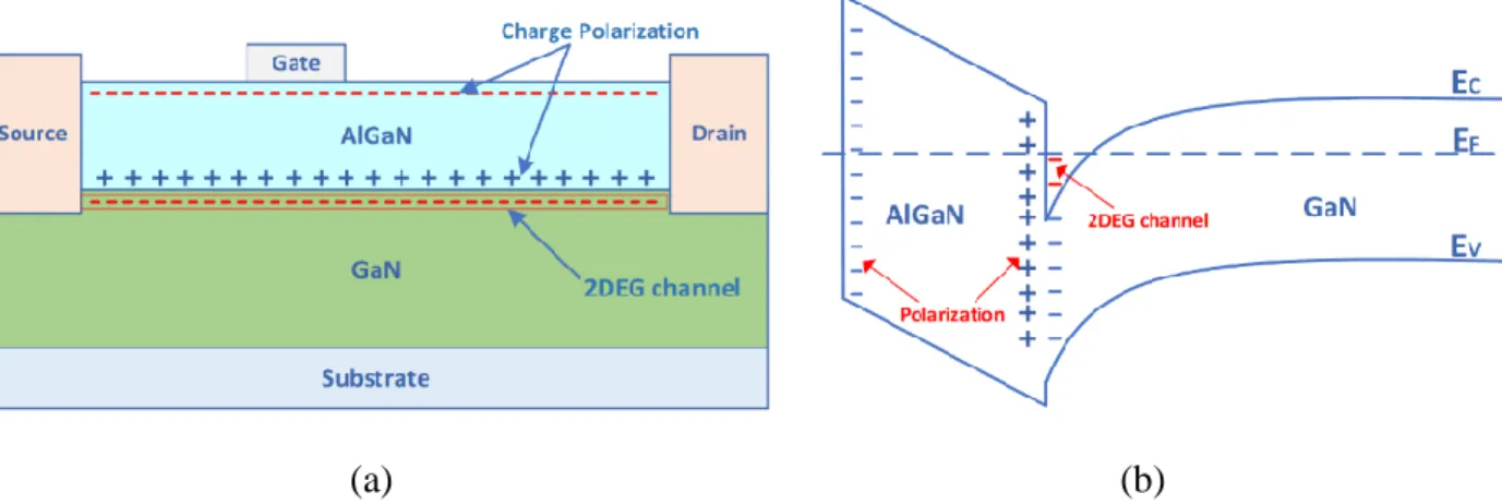
... 23 Figure 2.11: SiC JFET based circuit schematic of wireless sensing module for pressure and temperature measurement [50] ... 24 Figure 2.12: AlGaN/GaN based HEMT: a) Physical structure and b) Band structure ... 27 Figure 2.13: Schematic drawing of a typical GaN HEMT layer structure ... 28
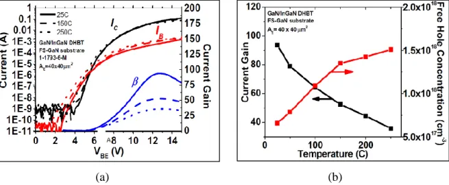
Figure 2.14: Semiconductor intrinsic carrier concentration versus temperature [62] ... 30 Figure 2.15: DHBT grown on a GaN substrate, a) Gummel plot, b) Common-emitter characteristic [109] ... 39 Figure 2.16: A measured Gummel plot of the DHBT at different temperatures, b) Measured current gain (β = IC / IB) and free hole concentration (p) calculated from 1/C2 v.s. VBE curve fittings
at different temperatures from 25 to 250 oC [111] ... 40 Figure 2.17: a) Photograph of a AlGaN/GaN HEMT. Three ohmic contacts (drain D and source S) and two finger Schottky contacts (gate G) at the top of the mesa are placed, b) Simple RoundHEMT layout with ohmic contacts (source and drain) and Schottky contact (gate) [59] ... 41 Figure 2.18: AlGaN/GaN HEMTs on Si and sapphire substrates: a) Temperature dependence of IDSS and peak of gm,ext normalized to their room temperature values, b) Dissipated
power-to-channel temperature transfer characteristics [59] ... 41 Figure 2.19: 0.25 × 50 μm2 AlIn/GaN HEMT device tested at 1000 oC: a) Sample under test, b)
I-V characteristics where I-VGS is swept from -8 V to 0 V by steps of 4 V [20] ... 42
Figure 2.20: Schematic cross section of an AlInN/GaN HEMT structure [20] ... 43 Figure 2.21: a) Cross section of NCD overgrown In0.17Al0.83N/GaN HEMT [115], b) Evolution of
the mean drain–source current (IDS,mean) with test time. (Inset left) Evolution of threshold
voltage (Vth) from RT up to 1000 oC. Small changes above 600 oC can be attributed to a slight
increase in the gate diode leakage current. (Inset right) SEM picture of the device, SiN passivation removed, after 25 h testing at 1000 oC. No visible damage can be observed [114] ... 44 Figure 2.22: Schematic of GaN HFET-based digital circuits. (a) Inverter block used in ring oscillator, and (b) Comparator [22]. ... 46 Figure 2.23: Schematic of GaN HFET-based integrated circuits. (a) Inverter, and (b) Differential amplifier [13]. ... 46 Figure 2.24: Proposed structure for making contacts in high-temperature devices ... 50
Figure 2.25: a) Modeled vs measured data for MIM capacitors [132], b) Resistance vs temperature range [133] ... 52 Figure 2.26: a) Measured inductance versus frequency, b) Modeled and measured Q versus frequency [134] ... 53 Figure 3.1: Not to scale cross-section of GaN HFET epitaxial layers. ... 61 Figure 3.2: Experimental setup of HT measurements. ... 62 Figure 3.3: HT packaging (at 600 oC): (a) HT wires connected to a DIL ceramic package, (b) Bonding wires between the pads of the chip and the package, (c) Wire bonding terminals on the package pads, and (d) Ball bonding on the chip pads. ... 63 Figure 3.4: Flowchart summarizing the HT modeling process. ... 66 Figure 3.5: Variations of two modeling parameters with temperature: (a) KT, and (b) P20. ... 67
Figure 3.6: Experimental and fitted output I-V characteristics at: (a) T = 25 oC, (b) T = 100 oC, (c)
T = 300 oC, (d) T = 450 oC, and (e) T = 500 oC. ... 68 Figure 3.7: Model validity tested for temperature values higher than the model calibration range: (a) At 550 oC, and (b) 600 oC. ... 69 Figure 3.8: Integrated passive components for HT characterization: (a) Resistors, and (b) Capacitors. ... 70 Figure 3.9: Variation of resistance slope with respect to the initial value of resistors. ... 71 Figure 3.10: HT characterization of different integrated resistors: (a) R5, (b) R6, (c) R8, and (d) R9.
... 72 Figure 3.11: HT characterization of different integrated capacitors. ... 73 Figure 3.12: Circuit structure of various digital logic gates: (a) NOT, (b) 2IN, (c)
NAND-3IN, (d) NOR-2IN, and (e) NOR-3IN. ... 74 Figure 3.13: Micrograph of implemented logic gates: (a) Inverter, (b) NAND-2IN, (c) NOR-2IN, (d) NAND-3IN, and (e) NOR-3IN. ... 75 Figure 3.14: Pulse characteristics of the inverter in the temperature range 25- 600 oC. ... 75 Figure 3.15: VTC of the GaN inverter (a) At 25C, and (b) Between 25 oC and 600 oC. ... 76
Figure 3.16: Measured dynamic characteristics of NAND gates: (a) NAND-2IN at 25 oC, (b)
NAND-3IN at 25 oC, (c) NAND-2IN at 300 oC, and (d) NAND-3IN at 300 oC. ... 77
Figure 3.17: Measured dynamic characteristics of GaN NOR gates: (a) NOR-2IN at 25 oC, (b) NOR-3IN at 25 oC, (c) NOR-2IN at 300 oC, and (d) NOR-3IN at 300 oC. ... 78
Figure 3.18: Integrated voltage references: (a) Schematic design, and (b) Micrograph. ... 79
Figure 3.19: Supply voltage dependence of the proposed voltage references in the temperature range 25- 600 oC: (a) VREF1, and (b) VRREF2. ... 79
Figure 3.20: Experimental voltage reference outputs in the temperature range 25- 600 oC. ... 80
Figure 4.1: Block diagram of the proposed power and data transmission system ... 85
Figure 4.2:Circuits of digital logic gates: (a) NOT, (b) NAND, and (c) NOR ... 87
Figure 4.3:Circuits of digital logic gates: (a) NOT, (b) NAND, and (c) NOR ... 87
Figure 4.4: Experimental (left) and simulation (right) results of NOT gate at 25 oC (T1) and 400 oC (T2) ... 88
Figure 4.5: Experimental (left) and simulation (right) results of NAND gate: (a) at 400 oC, (b) at 25 oC (OUT1) and 400 oC (OUT2) ... 88
Figure 4.6: Experimental (left) and simulation (right) results of NOR gate: (a) at 400 oC, (b) at 25 oC (OUT1) and 400 oC (OUT2) ... 89
Figure 4.7: Block diagrams of the proposed demodulators: (a) Half-bridge rectifier, (b) Full-bridge rectifier, and (c) Digital based ... 91
Figure 4.8: Building circuits: (a) Half bridge rectifier, (b) Voltage reference, (c) NAND (3IN), (d) D-Flip Flop, (e) Delay, and (f) Comparator ... 92
Figure 4.9: Comparator simulations at different temperatures: (a) Without adaptation, and (b) With adaptation ... 93
Figure 4.10: HBR demodulator simulation results at: (a) 25 oC, and (b) 400 oC ... 94
Figure 4.11: Digital demodulator simulation results at: (a) 25 oC, and (b) 400 oC ... 95
Figure 4.13: Chip layout view of the proposed data transmission systems ... 96 Figure 5.1: Block diagram of the proposed power and data transmission system. ... 103 Figure 5.2: Experimental setup for HT GaN500 device characterization. ... 105 Figure 5.3: Measured and simulated I-V characteristics of a GaN500 device at: (a) 25 oC; (b) 200
oC; (c) 300 oC; (d) 350 oC... 106
Figure 5.4: Integrated passive components for HT characterization: (a) Resistors; (b) Capacitors. ... 107 Figure 5.5: HT characterization of different integrated resistors: (a) R1; (b) R3; (c) R7; (d) R8. . 108
Figure 5.6: HT characterization of different integrated capacitors. ... 109 Figure 5.7: Data transmission system: (a) Block diagram of the transmitter; (b) Block diagram of the receiver; (c) Schematic of the amplifier; (d) Circuit diagram of the comparator; (e) Schematic of a 2-input NAND gate; (f) Schematic of a 3-input NAND gate; (g) Charge pump circuit; (h) Schematic of an inverter. ... 110 Figure 5.8: Amplifier simulated results at different temperatures. ... 112 Figure 5.9: Simulation results of the data transmission chain with the input in red and the output in blue at: (a) 25 oC; (b) 350 oC. The recovered Q an QB streams are plotted in the embedded graphs. ... 112 Figure 5.10: Comparator simulations at different temperatures. ... 113 Figure 5.11: D-Flip Flop simulation results: (a) Input signals; (b) Output Data. ... 113 Figure 5.12: Impact of the temperature on Charge pump during: (a) Charging; (b) Discharging.
... 115 Figure 5.13: Impact of the temperature on: (a) Oscillation frequency; (b) voltage transfer characteristics of the inverter. ... 115 Figure 5.14: Demodulator simulation results of input/output signals at: (a) 25 oC; (b) 350 oC. .. 116 Figure 5.15: Impact of the temperature on detected data (D) at: (a) 25 oC; (b) 350 oC. ... 117 Figure 5.16: Temperature impact on DELAY circuit. ... 117
LIST OF SYMBOLS AND ABBREVIATIONS
AC Alternating currentADC Analog-to-digital converter
ADS Keysight Advanced Design System ALD Atomic layer deposition
BEN Bias enhanced nucleation BiCMOS Bipolar-CMOS
BJT Bipolar junction transistor
CMOS Complementary metal-oxide-semiconductor COB Chip on board
CPFC Canadian Photonics Fabrication Center CTE Coefficient of thermal expansion DAC Digital-to-analog converter DBC Direct bond coper
DC Direct current
DD Displacement damage
2DEG Two-Dimensional Electron Gas DIBL drain induced barrier lowering DIL Dual in-line package
DHBT Double Heterojunction Bipolar Transistor
EG Energy bandgap
FBR Full bridge rectifier fc Carrier frequency
GaAs Gallium Arsenide GaN Gallium Nitride gm Transconductance HBR Half bridge rectifier
HFET Heterostructure Field Effect Transistor HEMT High Electron Mobility Transistor HT High-temperature
HTCC High temperature co-fired ceramic HVPE Hybrid vapor phase epitaxy HBT Heterojunction Bipolar Transistor IC Integrated circuit
IGFET Insulated-Gate Field Effect Transistor IMD Implantable medical devices
IPT Inductive power transfer JFET Junction filed effect transistor LSK Load Shift Keying
LTCC Low temperature co-fired ceramic MBE Molecular beam epitaxy
MESFET Metal semiconductor field effect transistor MIM Metal-Insulator-Metal
MOCVD Metal-organic chemical vapor deposition
MOSFET Metal oxide semiconductor field effect transistor
MOSHEMT Metal-oxide-semiconductor high electron mobility transistor MMIC Monolithic Microwave Integrated Circuit
Nc Effective electron density
NCD Nanocrystalline diamond ni Intrinsic carrier concentration
NRC Canadian National Research Council Nv Effective hole density
PCB Printed circuit board
Q Quality factor
RF Radio frequency
RFID Radio-frequency identification
RIE ECR Reactive ion etching with electron cyclotron resonance
RT Room temperature
RTD Resistive temperature detector SEE Single event effects
Si Silicon
SiC Silicon Carbide SiGe Silicon Germanium SOI Silicon on Insulator TC Transient coefficient
TCR Temperature coefficient or resistance TLP Transient liquid phase
TID Total ionising dose WBG Wide bandgap
LIST OF APPENDICES
Appendix A– Chip 1 ... 141 Appendix B– chip 2 ... 155
CHAPTER 1
INTRODUCTION
1.1 Motivation: wireless sensors in high-temperature applications
Several manufacturing industries, such as aerospace and aircraft engines, geothermal or oil and gas exploration need to measure physical properties under extreme temperature environment in real-time. These measurands may be pressure, temperature, strain, flame speed, acceleration, etc [1, 2]. In many cases, sensors placed in harsh environment are frequently isolated from their control or power management unit, which is usually located outside the harsh zone [3]. Commonly, these entities are interconnected with regular wires. However, drilling holes through the separation medium which is mostly metallic is not always an acceptable solution given the potential risk of toxic chemicals leakage, pressure or vacuum loss, and mechanical structure integrity weakening. In addition, these wired connections present many challenges for preserving system light weight, simplicity and low-cost system implementation. Therefore, a wireless power transfer and data exchange through metallic barrier without any physical penetration is in urgent demand for the harsh environment sensing field. However, few hundred degrees suffice for ruining the operation of a circuit. In fact, when the environmental temperature exceeds the conventional limit (higher than 125 ºC), traditional electronics are no longer able to fit their requirements. Unfortunately, this limitation in the conventional technologies negatively impacts the proliferation of many domains and industries.One of the proposed solutions to reduce the heating impact on electronics is to provide cooling systems. However, this additional thermal management solution introduces complexity and supplementary hardware. It adds wires, connectors, cooling tubing, special intakes, etc. Also, it increases overall weight and size which is not always acceptable or even feasible. Especially in critical applications such as aerospace where size, weight, and reliability should be optimized for achieving the required performance and lower the risks. Furthermore, the actual aerospace technological development does not leave much space for additional secondary systems. In fact, the number of installed sensors and microelectronic subsystems that control and monitor the critical parameters in vital high-temperature regions are intended to be increased in near future. Moreover, potential efforts are exerted to replace all hydraulic actuators and mechanical driven systems by electrical and electronic versions. These implemented electrical and electronic systems lower the
engine size and weight and require less maintenance compared to pumps, fluids, and vacuum piping. However, their wiring and connectors are exposed to harsh environment which is the principal cause of inspection and preventive maintenance on aircraft jet engines. Aiming to reduce wiring and corresponding accessories which adversely affect the system reliability, adopting a distributed electronic system architecture is an accepted approach in aircraft and automobiles applications. Still, having many wires is undesirable as they require shielding, routing, maintenance, additional size and weight. Consequently, the aerospace industry’s long-term vision pursues complete wireless control systems that can even harvest their required power from the surrounding extreme temperature. Achieving this vision would be a revolution in high-temperature applications giving birth to more reliable systems requiring no electrical wires. This would reduce space missions’ cost (1 kg of payload sent to space costs $20 000 US), extend deep-well drilling machine range (operational deep-drilling machines may reach 20,000 feet depth) and optimize weight, maintenance cost and fuel consumption in passenger aircrafts and automobiles. Therefore, the high-temperature electronics market is considered nowadays a niche market technology that can strongly affect the modern industrial fields.
For those reasons, worldwide influential aerospace industries like Safran Group, Airbus Defence & Space, etc. are seeking alternative microelectronic technologies developed to 1) sustain exceptional environmental conditions, 2) be installed in critical sensitive areas, 3) be implemented as microdevices, and 4) communicate wirelessly even through metal. Developing electronics tolerating such harsh environment while providing wireless communication would have a great economic impact on the extreme electronics market. The related high-temperature electronics market is still modest in commercial value compared to the worldwide market of conventional semiconductor technologies.
1.2 Wireless through metal
Several wireless solutions in ambient environment are proposed in the literature for through-metal-wall power and/or data transmission such as the RFID [4], the inductive coupling [5, 6], acoustic/ultrasound coupling [7], and capacitive coupling [8]. Capacitive couplings have very low power transfer efficiency, which makes them unsuitable for power delivery through metal walls. In an ultrasonic coupling, ultrasonic waves can propagate easily through various kinds of metals and allow both high-power transfer efficiency and high-data rates. However, exposition to extreme
high temperatures may alter the piezoelectric properties and consequently damage the functionality of ultrasonic transducers. On the other hand, inductive couplings can operate at temperatures far-exceeding the Curie point of piezoelectric materials and do not need a direct coupling with metal walls to provide a good transmission path, unlike piezoelectric transducers [3]. Using an inductive link allows power and data transfer without compromising the integrity of the physical structure. However, transferring AC magnetic fields through metallic medium presents few challenges to overcome. Due to the Faraday shielding and skin effects in metal, magnetic waves cannot effectively pass through metallic barriers, particularly those that have high electrical conductivity and magnetic permeability.
Nevertheless, systems relying on Inductive Power Transfer (IPT) has evolved in the last 20 years into a $1 billion industry [9]. Currently, the wireless energy transfer market is very dynamic. A wide range of products such as mobile phones in the lead, electric vehicles, robots, drones, and Implantable Medical Devices (IMD) use this technology.
1.3 GaN high-temperature technology
Silicon on insulator (SOI), gallium arsenide (GaAs) and silicon germanium (SiGe) are commercially available semiconductor technologies dedicated for high-temperature applications. However, they are serving a narrow range of temperatures not exceeding 300 oC, and are often associated with limited operation time, due to fundamental physical limitations of these semiconductors at high temperature [10]. Many significant industrial applications have requirements far exceeding this limit. For example, in turbine engines, many sensors and electrical actuators should be located in 600 oC ambient temperature. Similarly, in aerospace exploration, in addition to the extreme radiation environment that electronic must endure, the ambient temperature can exceed 500 oC. This is the case for Venus and Mercury exploration. Moreover, in geothermal
and automotive applications, telemetry devices and exhaust pipe sensors must sustain ambient temperatures above 500 oC.
Wide bandgap (WBG) semiconductors are considered as main candidates in the foreseeable future to overcome the fundamental limits of available conventional electronics in high ambient temperature applications. Silicon carbide (SiC) and gallium nitride (GaN) are the best-known WBG devices offering attractive features suitable for high temperature conditions such as wide bandgap
(3 eV), high drift saturation velocity, high thermal conductivity, low intrinsic carrier concentration and large critical electric field [10]. By contrast, silicon-based technologies are more mature and generally less expensive for a given line-width.
In general, both GaN and SiC belong to the same WBG semiconductors family and share similar attractive properties. However, SiC have received a great deal of attention in the past decade, especially in the high temperature applications field. Although important advances have been made on SiC based ICs, most of the reported ICs either had large areas or comprised small number of devices, leading to low device density integration [11]. In addition, no commercially available SiC integrated devices and circuits operating at temperature higher than 300 °C were found [12]. The direct temperature dependence of carrier concentration, due to the bulk nature of the active region in SiC devices, is considered as a common shortcoming [13] in addition to the crystal dislocations that degrade junction leakage, particularly at the highest temperature levels.
III-Nitride and primarily GaN technologies exhibit substantial performance improvement over SiC semiconductor with respect to response speed and operating temperature limits [14]. In addition, the temperature stability of electron concentration in the HEMT channel makes GaN devices more stable at high temperature. The recent research on GaN technology in Europe is summarized in [15] showing incremental progress to establish an independent GaN supply chain in Europe. In addition, [16]-[17] summarize some major recent trends of semiconductor research toward mature GaN technology that goes beyond the conventional limits of silicon. These papers discuss means to offer higher blocking voltages, wider range of operational temperature and better energy conversion efficiency.
Considerable efforts have been done to develop GaN devices operating at HT above 600 °C [14], 800 °C [18], 900 °C [19] and 1000 °C [20]. However, few research projects are directed toward the development of integrated microelectronic circuits and systems based on GaN devices. Despite the suitability of GaN technology for HT environments, limited integrated circuits and sensors are implemented based on GaN devices for HT applications [13], [21], [22]. The reported works show only the implementation of simple circuits like inverters, comparators, ring oscillators, and one stage differential amplifiers with maximum operation temperature not exceeding 500 oC. There are still many challenges with GaN based technologies, including material, ohmic and Schottky
contacts. These challenges should be overcome before the exceptional ability of GaN to function at extreme temperature exceeding 600 oC can be fully leveraged.
1.4 Objectives and research work overview
In this research, we propose the complete design of a wireless data transmission system to serve wireless monitoring sensors installed in harsh environments. Most of the existing industrial sensors impose bulky protection and direct connection between the monitoring sensor front end and the central control system. This is due to the limitations of available electronic technologies that can sustain high-temperature while processing the monitored data properly. To reduce the installation complexity and the protection cost, and to improve the data monitoring process, an appropriate technology should be developed and validated at HT. This technology will form the building blocks to implement circuits and systems able to operate in harsh conditions.
The primary goal of this thesis is to develop a data transmission system based on GaN technology to support wireless monitoring sensors and simplify their use in high temperature applications. Our specific objectives are:
Objective 1: Investigation and validation of GaN500 technology at HT: The selection of
GaN500 technology to implement the proposed system is based on special properties of GaN devices suitable for harsh environment conditions and the availability of GaN500 technology provided by NRC. The HT characterization of several GaN500 devices is performed to validate the robustness of the adopted technology at HT. An improved Angelov model is extracted from the HT characterization of GaN500 to capture the temperature effects on the design simulations. The HT model of integrated passive elements available in the GaN500 technology is also extracted from HT characterization and included in the design kit. This research was reported in Article 1.
Article 1: Hassan, A., Amer, M., A., Savaria, Y., & Sawan, M. High-Temperature
Characterization, Modeling and circuit validation of GaN500 HEMT up to 600 oC. IEEE
Transactions on Circuits and Systems I: Regular Papers, submitted (March 2019).
Objective 2: Design and implementation of GaN based building circuits: For the first time,
several digital and analog building circuits are implemented based on GaN500. These circuits form the building blocks of the proposed data transmission system. The normally-on depletion mode GaN500 devices impose significant design constrains which implies to use a minimum number of
transistors to obtain the desired functions and for better miniaturization of the complete system. In addition, three demodulators are implemented to recover the monitored data from LSK-based modulated signal. One of the demodulators is a fully digital demodulation system dedicated for high frequency data transmission (MHz range). While the other two demodulators are based on the rectification technique and are dedicated to low frequency data transmission (kHz range) mainly required for data transmission through metallic barriers. The functionality of implemented circuits and demodulators at HT is performed by simulation and by experimental measurements for some circuits. Article 2 is an outcome of the work conducted as part of objective 2.
Article 2: Hassan, A., Ali, M., Savaria, Y., & Sawan, M. GaN-based LSK demodulators for
wireless data receivers in high-temperature applications. Microelectronics Journal, published on 14 January 2019.
Objective 3: Design and implementation of fully integrated GaN based modulation and demodulation systems: The proposed modulation/demodulation system is the first GaN500-based
integrated data transmission system. Simple design with minimum number of transistors is implemented to reach a high integrity level and reduce the power consumption. The modulation system is based on a simplified delta-sigma modulation technique. The fully digital demodulator is adopted to recover the monitored data from the modulated signal. The reported simulation results confirm the functionality of the proposed systems using the models extracted from HT characterization. This work was reported in Article 3.
Article 3: Hassan, A., Ali, M., Trigui, A., Savaria, Y., & Sawan, M. A GaN-based Wireless
Monitoring System for High-Temperature Applications. Sensors, published on 14 April 2019. This paper was invited to the Special Issue on "Advanced Interface Circuits and Systems for Smart Sensors" in the Sensors Journal.
While pursuing Objectives 1 to 3, a number of additional publications listed below were produced.
Additional related articles:
Hassan, A., Savaria, Y., & Sawan, M. (2018). Electronics and packaging intended for emerging
harsh environment applications: A review. IEEE Transactions on Very Large Scale Integration
Hassan, A., Savaria, Y., & Sawan, M. (2018). GaN Integration Technology, an Ideal Candidate
for High-Temperature Applications: A Review. IEEE Access, 6, 78790-78802.
Conference proceedings:
Hassan, A., Trigui, A., Shafique, U., Savaria, Y., & Sawan, M. (2016, May). Wireless power
transfer through metallic barriers enclosing a harsh environment; feasibility and preliminary results. In 2016 IEEE International Symposium on Circuits and Systems (ISCAS) (pp. 2391-2394). IEEE.
Hassan, A., Ali, M., Trigui, A., Hached, S., Savaria, Y., & Sawan, M. (2017, June). Stability of
GaN150-based HEMT in high temperature up to 400° C. In 2017 15th IEEE International New
Circuits and Systems Conference (NEWCAS) (pp. 133-136). IEEE.
Abubakr, A., Hassan, A., Ragab, A., Yacout, S., Savaria, Y., & Sawan, M. (2018, May). High-Temperature Modeling of the IV Characteristics of GaN150 HEMT Using Machine Learning Techniques. In 2018 IEEE International Symposium on Circuits and Systems (ISCAS) (pp. 1-5). IEEE.
Amer, M., Hassan, A., Ragab, A., Yacout, S., Savaria, Y., & Sawan, M. (2018, May). High-Temperature Empirical Modeling for the IV Characteristics of GaN150-Based HEMT. In 2018
IEEE International Symposium on Circuits and Systems (ISCAS) (pp. 1-5). IEEE.
1.5 Organization of the thesis
This Ph.D. thesis includes seven chapters. The first chapter (Introduction) discusses the motivation behind this research. It also presents some background about wireless transmission through metal and the operation of GaN semiconductor. The primary and specific objectives are presented in this chapter as well, in addition to the organization of the thesis and coherence of the articles with the research goals.
In chapter 2, we present a critical literature review of harsh environment applications and the developed semiconductors to serve such applications including the advantages, challenges and limitations of each technology. This review introduces more specifically the problem formulation related to high-temperature devices and integrated systems for harsh environment applications. It
also shows the superiority of WBG GaN devices on other developed technologies at high temperature.
Chapter 3, 4 and 5 include our three scientific articles. In the first article (chapter 3), we demonstrate the performance of the GaN500 technology at HT including the characterization and modeling of fabricated GaN500 devices covering the 25 oC to 600 oC temperature range. The second article (chapter 4) presents the design and implementation of three demodulation systems based on GaN500 technology in addition to the circuit level validation of GaN-based digital circuits at 400 oC. In the third article (chapter 5), we present the complete design of a wireless data transmission system based on GaN500 technology including the description of the proposed system in addition to the main considerations about the adopted design kit.
Chapter 6 includes a general discussion that summarizes the work done in this research. It also discusses the main constraints and limitations of our work including the fabrication issues, packaging and HT testing.
Finally, chapter 7 summarizes our contributions and achievements in this project. It also includes our recommendations to be taken for further improvements on the present design as well as our suggestions for the future directions of the current research.
1.6 Coherence of the articles in relation to the research goals:
This thesis follows the article-based format that includes papers produced as part of this Ph.D. research. The proposed wireless data transmission system is introduced in chapters 3, 4 and 5 including the device characterization, modeling, circuit design and validation, as well as system design and implementation. Each one of the three chapters presents published or submitted research work. The articles are perfectly consistent with the research work in terms of complementarity and incrementality of proposed contributions.
In the first article, we intensively focused on the adopted technology to examine the maximum limit of GaN500 design kit reporting the electrical characteristics of devices and integrated passive elements as a function of temperature from 25 oC to 600 oC. This article is preceded by two review
articles and two conference papers. The review articles summarize the harsh environment applications and the corresponding developed electronics nominating the GaN devices as an ideal candidate for HT applications. The conference papers validate the possibility of transferring power
and data through metallic barriers at low frequency (kHz range) and show the robust HT characterization of GaN devices exceeding 400 oC. In the following two articles, the simulations at HT were performed using an Angelov model available in the GaN500 design kit. However, this model was not validated for temperatures higher than 350 oC. Therefore, in this article, an improved version of Angelov model is extracted to cover the 25 oC to 600 oC temperature range for future work. In addition, we experimentally demonstrated prototype digital logic gates and voltage reference ICs implemented using GaN500. The prototype ICs are characterized at operating temperatures ranging from 25 oC to 600 oC. This work contributes to the development and improvement of GaN technology, especially for GaN-based wireless monitoring systems targeting high-temperature environments. The reported GaN basic logic gates enable further development of other essential dynamic blocks such as ring oscillators, D-Flip Flop, delay elements and other typical digital logic circuits able to operate at HT.
The second article introduces the design of three demodulation systems based on GaN500 technology. The implemented systems demodulate LSK modulated signals for wireless monitoring applications operating at HT. The proposed demodulators are designed to demodulate low frequency modulated signals in the range of kHz and few MHz. The performed simulation results ensure their functionality over a wide temperature range between 25 oC and 400 oC. The design considerations of the proposed building circuits are discussed considering the specific requirements of the targeted applications and the limitations of adopted technology. Circuit validation of GaN-based logic gates was performed at 400 oC.
In the third article, we selected one of the three demodulators introduced in the second article to build the complete design of a wireless monitoring system. This wireless data transmission system is based on GaN500 technology that is proposed to acquire signals from sensors installed in HT environments. The HT characterization of GaN500 devices, integrated resistors, and integrated capacitors was performed to validate their corresponding models used in system simulations. Circuit simulations of subsystems and building blocks were performed over the 25 oC to 350 oC wide temperature range to validate the capability of the GaN technology to implement an integrated wireless system that can be used in harsh environment applications.
CHAPTER 2
LITERATURE REVIEW
2.1
Harsh environments and corresponding applications
Some harsh environments are more challenging than others. Among the different types of extreme conditions, the following are the most influential on the design and implementation of electronic devices and systems.
2.1.1 Low Temperature Environment:
The commercial temperature range specification of CMOS integrated circuits is from 0 °C to +85 °C, whereas the military specification temperature range is from −55 °C to +125 °C. In general, any temperature outside these ranges is considered an extreme temperature environment. Temperatures below those ranges are often called “cryogenic” due to the common use of cryogen liquids to reach them.
Diverse applications mandate cryogenic environments operation such as superconductivity. Further, many planetary bodies impose cryogenic environments, like the poles of Mars where the temperature drops below −143 °C in winter. Moreover, deep space applications, such the electronic detectors of the James Webb Space Telescope, operate at -246 °C.
Furthermore, in order to improve system sensitivity, diverse types of electronic instrumentations demand cryogenic temperatures as their operational temperature. Indeed, noise in resistors and electronic devices decreases with temperature and the dark current of diode detectors reduce exponentially with temperature. Thus, cooled detectors are found in various applications, such as in medical imaging instruments, high performance computers, satellite receivers and astronomical instruments.
2.1.2 High Temperature Environments:
On the other side of the extreme low temperature environments, extreme high temperatures surpass the standard commercial and military temperature range of +85 °C and +125 °C respectively. Indeed, many industrial applications require stable electrical and electronic systems for robust operation at high temperature. Aerospace electronic systems, automotive and on-engine
electronics, as well as power electronics are important examples where operating temperature ranges could extend up to 500 °C and even more if the electronic could withstand them.
Energy exploration such as geothermal production wells and oil and gas well-drilling are major applications of high-temperature electronics, where electronic systems must operate at temperatures ranging between 250 °C and 300 °C [23]. In addition, some space exploration projects mandate extremely high operating temperatures, which may exceed 600 °C, such as the missions targeting the surface of Venus.
2.1.3 Wide Temperature Range Environments:
A classic example of an environment imposing wide ranges of operating temperatures is the Moon, where its surface temperature in straight sunlight surpasses +120 °C, while dropping below -230 °C during the night, especially inside shadowed craters. The upper and lower limits of the temperature range in such applications may not by themselves be the worst factors to consider, but by the wide range covered and the temperature cycles in which the system must operate normally may be more harmful.
The rate at which thermal cycles occur may also be a significant issue and thermal shock can be far more challenging with respect to long-term reliability when compared to high or low fixed operating temperatures.
2.1.4 Radiation-rich Environment:
The three main categories of radiation effects are: a) displacement effects where high-energy particles displace atoms or nuclei, b) ionization effects where the materials are ionized when they are traversed by high-energy charged particles, and c) total dose that typically charges dielectric causing cumulative parametric shifts that render a device non-functional. Radiation-rich environments are mainly present in space applications, nuclear power plants and biomedical instruments.
2.1.5 Multi Extreme Environments:
When more than one type of extreme environments is present in one application, this situation will be called multi extreme environments. It is actually the most prevalent case as several harsh environments combine diverse types of extreme conditions, such as extreme low temperature with
extreme high pressure or vibration, or extreme high temperature combined with radiation-rich environments and so on.
Back to the Moon surface example, where low-temperature conditions (-230 °C) combine with high-temperature (+120 °C) and radiation effects due to solar winds and galactic cosmic rays, all these extreme environments must be addressed at once.
These diverse harsh environments and the corresponding applications stress the necessity of developing microelectronic devices that can meet application requirements in the expected environmental conditions. The following parts will investigate the most known semiconductors dedicated to harsh environments along with the corresponding limitations and improvements done so far.
2.2 Harsh environment electronics and implementations
Billions of dollars are invested in the extreme environment electronic industries to spread outside the conventional commercial and military electronics specifications. In 2005, the high-temperature electronics market was estimated to be around $17 billion. As a definition, extreme environment electronics are small volume systems with significant value-added propositions that are extremely important for harsh environment applications, but very costly to set and operate.
The following parts discuss the main existing electronic devices, along with their functionality at extreme environment conditions.
2.2.1 Silicon
Silicon based microelectronic technologies are the most common devices nowadays. Even though they are highly reliable in the majority of commercial applications, they are limited when the ambient conditions extend outside its normal -55 °C to +125 °C temperature range. Outside this interval, temperature can have a brutal impact on the transistor behavior. Once the surrounding temperature rises to extreme high ranges, the energy band gap of Si will drop down while the carrier density, which affects the thermal and electrical conductivity, exponentially increases, turning from stable extrinsic region into the intrinsic region. Another sensitive parameter affected by temperature variation is mobility, which determines the drift speed of a particle subject to an applied electric field. Moreover, the current density, carrier diffusion, velocity saturation,
electromigration, leakage current, threshold voltage and interconnect resistance are all significant mechanisms or parameters directly affected by extreme temperatures.
Another set of considerations with Si based platforms is their sensitivity to radiation. Even though threshold voltage shift with total dose is a dielectric volumic effect that had reduced significantly with scaling, the subthreshold leakage current is still seriously affected with deep submicron technologies. More precisely, gamma rays, cosmic ray’s ions, x-rays, neutrons as well as high-energy electrons and protons have significant effects on electronic circuits operation that can have major impacts on operating characteristics and may induce failures.
The main basic concepts used to express and model the interaction between Si devices and radiation are the total ionizing dose (TID), displacement damage (DD) and single event effects (SEEs). TID is the damage produced by ionizing radiation over a time interval. Electron-ion pairs are generated by this ionizing radiation inducing trapped charges which, in turn, produce transient and long-term effects, in addition to changing threshold voltage and current leakage path. The displacement damage (DD), which is resulted by heavy ions, alpha particles, protons, neutrons and very high energy photons, can modify the configuration of the atoms in the semiconductor. It may provoke a permanent damage augmenting the recombination centers number and lowering the minority carriers. SEE is caused by a high-energy particle passes through a semiconductor keeping an ionized path behind. When this charge moves, it might be collected to another charge resulting in serious effects starting by a bit-flip and ending by tragic burnout.
2.2.2 Silicon on Insulator
Silicon-on insulator (SOI) technology is an advanced alternative option of the silicon CMOS technology to mitigate the drain induced barrier lowering (DIBL) and restrain charge-sharing and fringing field effects especially for the short-channel CMOS platforms and more precisely in 45 and 65 nm technologies.
SOI is mainly dedicated for aerospace and military applications exploiting its rigidity against the extreme temperature and radiation environments. Nowadays, it is more accepted as a commercially available technology.
SOI CMOS family is the most mature approach using traditional silicon process but includes an isolation process to ultimately reduce the leakage current at high temperature. Comparing to the
conventional P-N junction isolation in Si CMOS technology, a silicon dioxide layer surrounds each SOI transistor giving an excellent electrical isolation characteristic even at high-temperature conditions [24].
Figure 2.1: CMOS SOI based voltage reference circuit [25]
Consequently, SOI CMOS device was successfully implemented to serve a universal gate driver circuit at temperature higher than 200 oC [25] and utilized in voltage reference circuit (shown in Figure 2.1) for a range of temperature between -40 oC and 200 oC under total radiation dose of 1 Mrad [26]. In addition, Honeywell investments in high-temperature SOI electronics introduced several products and processes like opamps, voltage references, voltage regulators, analog multiplexors, A-to-D converters (shown in Figure 2.2), digital gate arrays, SRAM, 8-bit microprocessor and clock interfaces [27] with endurable temperature exceeding 200 oC.
Another advantage of SOI appears in the omission of parasitic area junction capacitance and the decrease of cross talk between digital and RF circuitry, in addition to the adequacy to integrate passive elements on chip with high accuracy profiting from the large substrate resistivity. Other merits for the SOI are the reduction of a reverse body effect in stacked circuits and the junction of the floating-body with source and drain is usually forward-biased.
Figure 2.2: SOI based 12-bit analog-to-digital converter [27]
The SOI flexibility with the radiation is returned to its geometric constrains limiting the volumes of active silicon regions with the radiation energy ionization and deposition, and the limited communication of deposited charge between the devices.
SOI MESFET (Metal semiconductor field effect transistors) is a different approach for the silicon on insulator technology which is also developed to support the extreme environment applications covering a wide range of temperature between -180 °C and +300 °C and enduring intense radiation dose as shown in Figure 2.3(a) and (b) respectively [28]. The MESFET implementation, as shown in Figure 2.4, requires a Schottky barrier which is composed of the silicide step providing the low resistance source–drain contacts. The gate silicide is isolated from the source-drain silicides by space regions of length LaS and LAd [29]. The silicide–silicon interface has the advantage of being
extremely stable up to relatively high temperatures. Table 2.1 shows the utilized protection in each presented SOI devices.
(a) (b)
Figure 2.3: MESFET SOI CMOS technology as a function of gate voltage (V) for a fixed drain bias of 2 V: a) The drain current (left) and gate current magnitude (right) of 600 nm gate length, b) The radiation response of 300 nm gate length MESFETafter successive radiation exposure up
to a TID of 300 krad(Si) where the MESFET was positioned at a distance from the 60Co source
that gave a dose rate of 0.9 krad(Si)/min [28]
Figure 2.4: Schematic cross section of the SOI MESFET [29]
The insulating regions of SOI are mainly achieved by SiO2 deposits. Regretfully, this isolation
layer has a thickness more than that of the gate itself and suffers a charge trap higher than the highly-optimized gate stacks resulting in radiation responses by these isolation regions. To clarify this, the buried insulating oxide and associated TID for a thin SOI device can be represented as a secondary gate. This secondary gate modulates a pseudo-channel at the bottom of the transistor producing backside leakage current or attaches to the top surface channel by electrostatic force modifying the transistor threshold voltage. Moreover, even for the modern SOI technology such as
vertically stacked structures and mutli-gate which are intended for harsh environments, the parasitic effects have significant impacts.
2.2.3 Silicon Germanium (SiGe)
SiGe is a BiCMOS technology implemented by adding heterojunction bipolar transistor (HBT) to Si CMOS platform. This implementation advocates the functionality of highly integrated system performing a mixed-signal technology which is qualified by its high-performance feature for RF, analog and microwave circuits. The most preferable SiGe approach for extreme environment applications is the complementary SiGe BiCMOS on a thick-film SOI substrate to perform noise isolation which presents a critical topic in various analog and mixed-signal systems.
With decreasing temperature, the Si BJT device suffers from degradation in the turn-on voltage junction, base resistance, current gain, frequency response, cutoff frequency and delay in digital circuits. Unlike the Si BJTs, the cooling impact (low temperature environment) on SiGe HBT device is favorably improving its dc and ac properties [30]. A simple check of the SiGe HBT device equations shows the improvement in the transconductance, current gain, cutoff frequency, maximumfrequency and broadband noise [31, 32].
In fact, despite the performance degradation of Si BJTs in cryogenic conditions, the addition of SiGe dramatically changes the situation. The bipolar transistor properties will be strongly coupled to the band-edge effects induced by bandgap engineering. Physically, the minority carrier of bipolar transistor is the reason of this strong coupling which implies in terminal currents proportional to the intrinsic carrier concentration (ni02) through the Shockley boundary conditions, and in turn ni02
is proportional to the exponential of the bandgap. Therefore, the currents will be coupled exponentially with any changes to the bandgap [30].
Moreover, from general mechanical considerations, these bandgap changes will automatically be divided by the thermal energy (kT), which means that a reduction in applied temperature will considerably increase any bandgap changes. Consequently, SiGe HBT device equations inspire that both ac and dc properties are favorably influenced by cooling.
Comparing the equations of a SiGe HBT to a comparably constructed Si BJT, the thermal energy (kT) is arranged to favorably affect the low-temperature properties. An extensive discussion with detailed analysis can be found in [33].
(a) (b)
(c) (d)
Figure 2.5: SiGe HBT: a) Cross-sectional view (3rd generation), b) Current–voltage characteristics (1st generation), c) Current-voltage characteristics (3rd generation) exposed to
space-relevant 63-MeV protons to multi-Mrad total dose, and d) Cutoff frequency for four generations before and after exposure to space-relevant 63-MeV protons to multi-Mrad total dose
[30]
On the opposite side of cryogenic conditions, the high-operating temperature has a degradation effect on both dc and ac performance of SiGe HBTs. However, the degree of this degradation is a matter to be discussed and investigated. Accordingly, SiGe HBTs commercially available with current gain above 100 and cutoff frequency of 75 GHz normally operate at 300 oC [34]. In addition to the robustness of SiGe HBT device at extreme low and high temperatures, the durability of this
device in radiation environment has been investigated as well [35] showing a favorable built-in TID great tolerance as presented in Figure 2.5(c) and (d).
SiGe HBT, illustrated in Figure 2.5(a) with its unique bandgap properties, presents a significant process for the extreme environment applications. The latter can be classified as following: extreme high-temperature conditions exceeding 300 °C as characterized in Figure 2.5(b), extreme low-temperature environments lower than -200 °C (Figure 2.6) [30], wide and cyclic low-temperature intervals such as the lunar surface temperature between -230 °C and +120 °C, and finally the intense radiation environments.
(a) (b)
Figure 2.6: Output characteristics of a SiGe HBT (first-generation) operating at a) T = 27 oC, and b) T = -230 oC [30]
As an example, the work in [36] was supported from NASA ETDP to develop a remote electronics unit system based on SiGe HBT. The implemented remote sensor interface is depicted in Figure 2.7. The implemented system was tested under cryogenic temperature less than -173 oC, 100 krad TID radiation exposure and at high temperature of 125 °C. Therefore, SiGe HBT is capable to satisfy the electronic requirements of all the preceding extreme environment conditions by slight process modifications providing considerable benefits regarding the weight, size and power constraints.
Moreover, in [37] and [38] SiGe devices have been utilized to implement voltage reference and LNA circuits respectively for cryogenic applications. Similarly, a wide-range temperature test (from -180 °C to 120 °C) have been successfully applied to ADC [39] and DAC [40] respectively.
Diverse generations of SiGe are nowadays widely spread in the commercial communities with tens of fabrication companies. The frequency capability of available SiGe HBT is between 50 and 200 GHz. Recently, 90 nm SiGe BiCMOS technology was presented in a comparator circuit for wide temperature range application between -195 oC and -155 oC [41], and a fourth generation of this device is implemented in [42] for RF applications at cryogenic temperature exceeding -195 oC. Table 2.1 shows the utilized protection type in each presented SiGe device [30], [33-42].
Figure 2.7: SiGe BiCMOS (SiGe HBT + CMOS) based simplified block diagrams of the Remote Sensor Interface [36]
Table 2.1: Protection type of presented SOI and SiGe devices
Device Reference Protection SOI
[25] Ceramic package + Polyimide test board
[27] Ceramic package + Al-wire bonding + Au-plate + Ni-bond pad [26], [28, 29] N/A
SiGe
[30, 33, 36]
Multi-chip Module Packaging: Al2O3 pacakge and lid, AlN
substrate, Cu metallization, Au wire bond, In/Pb lid seal, polyimide and Cryogenic ribbon cable
[34, 35], [39, 40] N/A
[37] Ceramic flat package [38]
PC board sandwiched in between two gold plated brass carriers with the IC mounted in a VIA hole to minimize bond wire lengths
[41] Simulation
[42] Custom-designed, on-wafer, open-cycle liquid nitrogen (LN2) probe station
![Figure 2.8: Cross-sectional view of the two basic SiC MOSFET: a) Inversion-channel, b) Doped- Doped-channel [12]](https://thumb-eu.123doks.com/thumbv2/123doknet/2332742.32089/45.918.180.744.344.622/figure-cross-sectional-mosfet-inversion-channel-doped-channel.webp)
![Figure 2.10: 6H-SiC JFET: a) Current–voltage characteristics, b) NOT gate IC test waveforms [45]](https://thumb-eu.123doks.com/thumbv2/123doknet/2332742.32089/46.918.157.762.372.699/figure-sic-jfet-current-voltage-characteristics-gate-waveforms.webp)
![Figure 2.11: SiC JFET based circuit schematic of wireless sensing module for pressure and temperature measurement [50]](https://thumb-eu.123doks.com/thumbv2/123doknet/2332742.32089/47.918.163.749.365.695/figure-circuit-schematic-wireless-sensing-pressure-temperature-measurement.webp)
![Figure 2.15: DHBT grown on a GaN substrate, a) Gummel plot, b) Common-emitter characteristic [109]](https://thumb-eu.123doks.com/thumbv2/123doknet/2332742.32089/62.918.138.784.619.894/figure-dhbt-grown-substrate-gummel-common-emitter-characteristic.webp)
![Figure 2.19: 0.25 × 50 μm 2 AlIn/GaN HEMT device tested at 1000 o C: a) Sample under test, b) I- I-V characteristics where I-V GS is swept from -8 V to 0 V by steps of 4 V [20]](https://thumb-eu.123doks.com/thumbv2/123doknet/2332742.32089/65.918.118.807.621.944/figure-alin-hemt-device-tested-sample-characteristics-steps.webp)
![Figure 2.21: a) Cross section of NCD overgrown In 0.17 Al 0.83 N/GaN HEMT [115], b) Evolution of](https://thumb-eu.123doks.com/thumbv2/123doknet/2332742.32089/67.918.119.806.392.693/figure-cross-section-ncd-overgrown-gan-hemt-evolution.webp)

![Figure 2.26: a) Measured inductance versus frequency, b) Modeled and measured Q versus frequency [134]](https://thumb-eu.123doks.com/thumbv2/123doknet/2332742.32089/76.918.168.752.307.556/figure-measured-inductance-versus-frequency-modeled-measured-frequency.webp)