HAL Id: hal-03020561
https://hal.archives-ouvertes.fr/hal-03020561
Submitted on 23 Nov 2020
HAL is a multi-disciplinary open access
archive for the deposit and dissemination of
sci-entific research documents, whether they are
pub-lished or not. The documents may come from
teaching and research institutions in France or
abroad, or from public or private research centers.
L’archive ouverte pluridisciplinaire HAL, est
destinée au dépôt et à la diffusion de documents
scientifiques de niveau recherche, publiés ou non,
émanant des établissements d’enseignement et de
recherche français ou étrangers, des laboratoires
publics ou privés.
Excitation of Symmetry Protected Modes in a Lithium
Niobate Membrane Photonic Crystal for Sensing
Applications
Ayman Hoblos, Miguel Angel Suarez, Nadège Courjal, Maria-Pilar
Bernal-Artajona, Fadi Baida
To cite this version:
Ayman Hoblos, Miguel Angel Suarez, Nadège Courjal, Maria-Pilar Bernal-Artajona, Fadi Baida.
Ex-citation of Symmetry Protected Modes in a Lithium Niobate Membrane Photonic Crystal for Sensing
Applications. OSA CONTINUUM, 2020, 3 (11), pp.3008-3018. �hal-03020561�
Excitation of Symmetry Protected Modes in a
Lithium Niobate Membrane Photonic Crystal for
Sensing Applications
A
YMANH
OBLOS,
1,*M
IGUELS
UAREZ,
1N
ADÃ
´LGEC
OURJAL,
1M
ARIA-P
ILARB
ERNAL,
1 ANDF
ADII. B
AIDA11Institut FEMTO-ST, UMR CNRS 6174, UniversitÃľ Bourgogne Franche-ComtÃľ, 25030 BesanÃğon cedex,
France
*ayman.hoblos@femto-st.fr
Abstract: Our theoretical study reveals the opportunity to develop an electric field sensor based
on the exploitation of Symmetry Protected Mode (SPM) that we excite within an electro-optical material, namely lithium niobate (LN). The SPM consists of a dark Fano-like resonance that results from the combination of a discrete Bloch mode of a Photonic Crystal (PhC) with a continuum mode of a membrane, both of them made in LN. The dark character is linked to the structure geometry having a high degree of symmetry. The SPM excitation is then made possible thanks to an illumination under small oblique incidence which breaks the symmetry of the configuration. This results in several ultra-sensitive and tunable Fano-like resonances with high quality factors up to 105in the telecoms spectral range. Some of these resonances provide
modes with a highly confined electric field inside LN. This confinement allows the enhancement of the electro-optic Pockels effect by a factor up to 4 × 10⁵, thus exacerbating the detection
sensitivity of the designed sensor.
© 2020 Optical Society of America under the terms of theOSA Open Access Publishing Agreement
1. Introduction
Today, the world faces a large number of challenges in different disciplines such as health, data processing, energy, information flow and environment. The growing demand for high sensitivity of detection in medical, military and other applications, has led to the emergence of new and impressive solutions to detect weak signals. Photonic technologies and in particular Photonic Crystals (PhCs) are one of the most important solutions in sensing applications. They are now widely used for the design of electric field sensors (E-field sensors) [1], magnetic field sensors [2, 3], temperature sensors [4–6], gas-sensors [7, 8] and other biological sensors [9, 10]. Several physical phenomena can be exploited for the detection of these quantities. Let us quote for example the piezoelectric effect [11], the photorefractive effect [12], the conductive and inductive effects [13, 14], the pyroelectric effect [15]... In optics, and to avoid the use of very powerful light sources, it is often convenient to rely on a linear effect. The Pockels effect perfectly fulfills this condition because it allows, through an electro-optical (EO) material, to induce a change in the optical properties of the material that is linearly linked to the E-field to be measured. We focus in this paper on the E-field sensors based on PhC engraved within highly efficient EO medium.
However, when compared with traditional electronic technology, E-field sensors based on metal-free structures offer several advantages because of their excellent electrical insulation [16, 17]. They are much more compact, which results in a higher stability and less distortion to the E-field distribution [18].
The conventional principle of an EO sensor is as follows: an external E-field induces the modification of the refraction index of the material. This modification leads to a redistribution of the electromagnetic field inside the material and, consequently, modifies its optical properties that are detected by reflection or by transmission. The key-point is then to design a configuration
where this distribution is important enough to allow the detection of very weak signals. This can be achieved by highly confining the electromagnetic density of states [19].
In this context, several studies were conducted showing different configurations with a high aptitude to detect weak signals. Roussey et al. [20] present a simple structure of PhC made of air holes engraved into a lithium niabate (LN) waveguide. They show a theoretical and experimental photonic band gap shift 300 times larger than expected through a non-structured waveguide (without PhC). To bypass the experimental drawbacks due to the light injection into waveguides, Qiu et al. [21] proposed to excite membrane PhC Fano resonances at normal incidence. In that study, Fano resonance is obtained by coupling a discrete Bloch mode of a PhC with a continuum mode of a LN membrane. They got a sensitivity of ∆λr es/∆E= 0.25 × 10⁻⁵nm.m/V.
As in the studies cited above, we will choose the LN as an active material, due to its high EO coefficient with high transparency in the visible and infrared wavelength regime [22–24]. LN is well known for its high nonlinear optical coefficients, piezoelectric, ferroelectric and large acousto-optic coefficient [25].
Seeking a configuration exhibiting a resonance with high quality factor, we came across the symmetry protected mode (SPM) [26–28]. This kind of resonance provides an excellent electromagnetic field confinement essential to enhance the LN EO effect surpassing a conventional Fano resonance [21]. As it is well-known [29, 30], SPM generally occurs when a structure with a high degree of symmetry is assumed. The excitation of such modes needs a small break of this symmetry which has an important impact on their resonance Q-factor. For example, a square grating photonic crystal with an elementary pattern, having a perfectly symmetrical shape with an axis of symmetry parallel to the incident beam, is an excellent candidate for exhibiting such modes. At normal incidence, these modes still are dark ones. At oblique incidence, such SPM turns into bright modes and can be easily excited. The dark character of such modes can be seen as a destructive interference (quality factor tends to infinity) between more than two degenerated modes. SPMs have recently been used to demonstrate high-quality factor resonances near normal incidence (more than 109) that may be exploited for various applications [31, 32]. Therefore,
motivated by the SPM, we propose to excite such dark modes by introducing a small symmetry breaking through the illumination direction.
Our theoretical studies reveal the opportunity to develop an E-field sensor based on a tunable resonance with a high Q-factor (up to 1.2 × 10⁵) and a robust extinction factor of 60%. We reach a new horizon with our structure due to an intensity enhancement that locally reaches 60000. This allows a detection sensitivity of 4 pm.m/V, 160000 times greater than the sensitivity obtained through a Mach-Zehnder interferometer design [22] and 1600 times greater than what was predicted with a membrane PhC Fano resonance [21].
2. The Proposed Structure
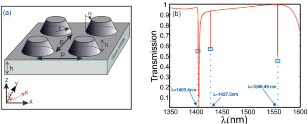
First, as in refs. [1, 21], we choose a configuration based on a PhC operating near the Γ direction (out-off-plane illumination around normal incidence). For an efficient detection, the PhC period must be smaller than the operation wavelength providing only one direction (only the diffracted zero-order is propagative) for the reflected and transmitted energy. This condition is fulfilled, at normal incidence illumination when p < λ, with p being the period of the structure and λ is the operating wavelength.
To excite Fano SPM resonances, we propose a PhC, which supports spectrally discrete Bloch modes, to be combined with a membrane which allows the existence of broadband guided modes. If we illuminate the membrane at normal incidence, no guided modes can be excited due to the perfect axial symmetry (counter propagating modes). Nonetheless, as shown on Fig. 1(a), the cylindrical symmetry of the PhC patterns together with the square symmetry (C4 axis) of the Bravais lattice keeps prohibited the excitation of the guided modes at normal incidence. Fortunately, an oblique incidence can lift this ban and lead to the excitation of some dark guided
Fig. 1. (a) Schematic of the proposed structure, (b) the transmission spectrum of the complete structure.
modes. The signature of this excitation is then a sharp resonance (dip for instance) in the transmission spectrum of the structure (see Fig. 1(b)). Moreover, working with a small angle of incidence yields to a small break in the symmetry of our structure. The smaller the angle of incidence, the greater the Q-factor of the resonance.
Consequently, our structure relies on a square lattice PhC of period px = py = p = 1050
nm. The unit cell consists of a truncated conical rod with a base’s radius r= 0.3 × p, a height h = p/3 = 350 nm and a conicity angle α = 15oengraved within a LN layer of 2 × h= 700 nm thickness as presented in the schematic of the structure in Fig. 1(a). The fabrication of the structure has been studied previously in detail by G. Ulliac et al. [34]. The conical rods (PhC) are usually fabricated by Focused Ion Beam (FIB) milling, which is highly time consuming. G. Ulliac et al. proposed an easy to implement batch technique consisting of writing these patterns by e-beam lithography followed by Reactive Ionic Etching.
The higher EO coefficient of LN is the r33one that involves the E-field component parallel
to its optical axis. To benefit from this coefficient when illuminating the material at normal incidence, we should use a X- or Y-cut wafers of LN (the optical axis is then parallel to the electric incident field). Furthermore, as a first approximation, one can neglect the other EO coefficients of LN and write the optical refractive index modification induced by the presence of an external electric field Esthrough [35]:
∆n(x, y, z) = −1 2× n
3
e× r33× Es (1)
with ne= 2.21 is the extraordinary optical index of LN at 1.55 µm. The structure is illuminated
by a linearly polarized plane wave at oblique incidence (see angle θ in Fig. 1(a)). The optical response is calculated using a home-made code based on the finite-difference time-domaine (FDTD) method [36] with an oblique incidence (θ= 0.5◦). The transmission spectrum shows several sharp resonances (at least 4 resonances between λ= 1350 nm and λ = 1600 nm) as shown in Fig. 1(b).
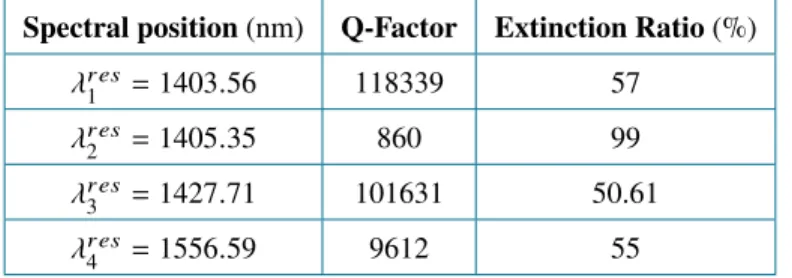
In order to point out the origin of these resonances, we have studied the optical response of the PhC and the LN membrane separately. The obtained spectra (not presented here) show a single sharp Bloch mode resonance with a Q-factor= 5480 for the PhC while an almost flat transmission coefficient is obtained for the membrane (continuum). Fortunately, by coupling the two structures, additional sharp resonances appear whose correspond to some dark modes (SPMs) that are excited thanks to the symmetry-breaking induced by the oblique incidence illumination. The properties of the resonances in the spectral range λ ∈[1350 nm;1600 nm] are summarized in
table 1 in terms of Q-factor and Extinction Ratio. The latter is defined by: Extinction Ratio=Tmax− Tmin
Tmax
(2) where Tmaxis the maximum transmission value just near the resonance dip and Tminis the
minimum transmission value at resonance. Note that a high Q-factor generally corresponds to high electromagnetic density of state, which is consisting with the origin of SPMs.
Table 1. The properties of the four resonances of the transmission spectrum presented in Fig. 1(b).
Spectral position (nm) Q-Factor Extinction Ratio (%)
λr es 1 = 1403.56 118339 57 λr es 2 = 1405.35 860 99 λr es 3 = 1427.71 101631 50.61 λr es 4 = 1556.59 9612 55
Otherwise, for λr es2 , the relatively low Q-factor indicates a resonance with a slightly confined mode, which can’t match an SPM. In the following, this mode will no longer be analysed since it is considered to be unsuitable for the EO detection application.
The transmission spectrum for the coupled structure is difficult to be quantitatively understood, but the origin of the SPM resonances is most likely linked to the interference of the PhC Bloch modes with the dark modes (guided modes) of the membrane or vice versa. This will be discussed in more details in the next section.
3. Results and Discussion
While some modes (bright modes) are excitable at normal incidence, others (dark modes) remain inaccessible due to structure symmetry. For out of normal incidence, the broken symmetry induced by this propagation direction triggers the selection rules and enables the excitation of SPMs. Moreover, the break of the symmetry can induce the degeneracy of some modes and remove it to some others. It makes dark modes become bright or vice versa (case of the Bound state In the Continuum (BIC) modes) [28].
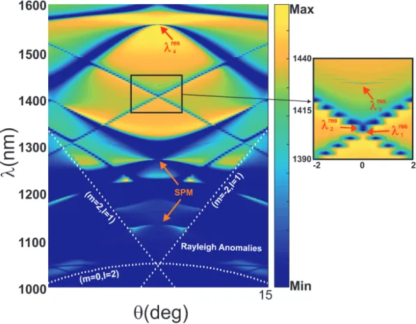
To confirm the nature of our three SPMs, we present on Fig. 2 the angle-dependence transmis-sion diagram calculated using the FDTD algorithm [39] for an incident TM-polarized plane wave. This diagram exhibits many sharp resonance features between λ= 1000 nm and λ = 1600 nm. One can clearly see the extinction of some resonances at some critical angles and the appearance of others. In a general way, the resonances marked by red arrows show vanishingly narrow transmission dips as θ approaches 0◦, except λr es2 . It shows an invarariant transmission behavior versus θ. Therefore, with a small variation of θ, one can achieve resonances with a huge Q-factor. By increasing the angle of incidence the resonances become too wide and the Q-factor gradually decreases [28]. The resonance suppression at θ= 0◦can be seen as destructive interference of emitted diffracted fields from two opposite sides of the symmetric structure. Let us mention that, due to the fabrication imperfections (residual roughness for instance), SPMs could be excited even at normal incidence. In that case, the Q-factor, that is related to the degree of the symmetry breaking, only depends on the preciseness (resolution) of the nano-fabrication process [37].
Fig. 2. Transmittance to the power of five (T5instead of T to enhance the visibility of the different resonances) as a function of wavelength λ and angle of incidence θ in TM-polarization. The white dashed lines correspond to the Rayleigh anomalies calculated using the Eq.1 in [38]. The four resonances of table 1 are indicated in red arrows but other SPMs appear for smaller values of the wavelength (see ochre arrows). A zoom-in of a the part framed by a rectangle is made on the right part of the figure to point out the two close resonances λr es1 and λr es2 .
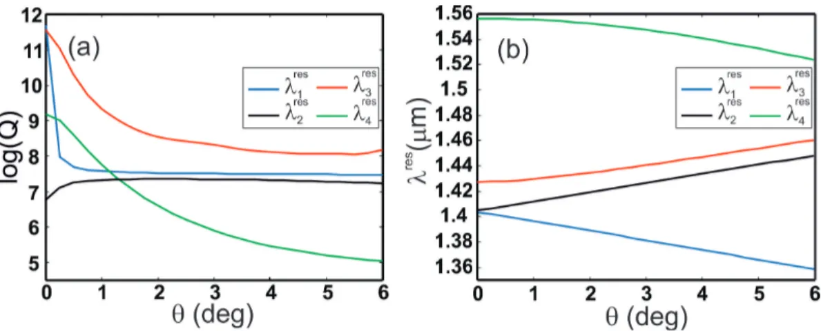
In order to show more details about the SP properties of the four resonances indicating in Fig. 1(b), we extract from the diagram of Fig. 2 their Q-factor and spectral position variations with respect to the angle of incidence as shown in Fig. 3. On the first hand, Fig. 3(a) denotes that the Q-factor of the resonances for λr es
1 , λr es3 and λr es4 exhibits a quite similar decreasing behavior
when θ increases meaning a similar origin, namely SPM. Contrarily, for λr es2 , a different behavior is obtained with a Q-factor that slightly grows but remains almost invariant for increasing angle of incidence (see the black triangles). On the second hand, Fig. 3(b) shows different behaviors for the spectral position with respect to the angle of incidence even for SPMs. More precisely, the spectral position for resonances at λr es1 and λ3r esincreases with the angle of incidence θ while they do not have the same origin. So, the evolution of the spectral position of the resonances does not give a discriminating information on the origin of the resonance.
In order to choose the most efficient resonance for our application (E-field sensing), we examine the influance of the electric field confinement on the electro-optical effect. The local expression
Fig. 3. (a): Evolution of the quality factor for different resonances in algorithmic scale with respect to the angle of incidence. (b): Evolution of spectral position of resonances with respect to the angle of incidence.
of the latter is then derived from Eq. 1 as [21]: ∆n(x, y, z) = −1
2 × n
3
e× fop2 (x, y, z) × r33× Es (3)
where fop(x, y, z) is the local optical field factor defined by
fop(x, y, z) =
| ®E(x, y, z)|str uctur e
| ®E |bulk
, (4)
where | ®E |bulkis the amplitude of the homogeneous E-field in the bulk structure (without PhC)
and | ®E(x, y, z)|str uctur eis the local amplitude of the E-field in the studied structure. Thus, it
is essential to consider the SPM mode for which the fop is most important. Nonetheless, as
the electro-optical effect is a property of the dielectric media, we are seeking resonance which corresponds to a "dielectric mode" for which the confinement of the E-field occurs inside the electro-optical material (LN for instance). When the confinement of the E-field is outside the structure (in the air), it is called "air mode".
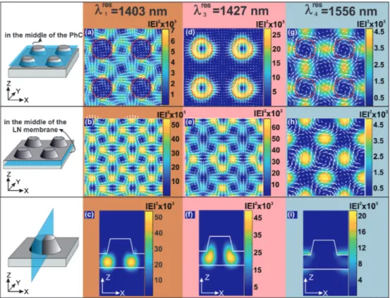
To fulfill these two conditions, we calculate the E-field distributions inside and around the structure for the three SPMs (at λr es
1 , λ3r esand λr es4 ). Fig. 4 show these distributions in XY and
X Z plans associated to each resonant wavelength pointed by a blue square in Fig. 1(b). The first column of Fig. 4 shows the plans (in blue color) where the electric intensity is calculated. The second column of fig. 4 corresponds to the resonance at λr es1 = 1403 nm. From Fig. 4(a), that corresponds to the E-field intensity in a plan cutting the conical patterns at their mid-height, one can see the occurrence of three E-field vortices per period. The rotating character of the electric field (see the white arrows) denotes a symmetry which is inconsistent with a linearly polarized plane wave near normal incidence. This behavior appears even more clearly in Fig. 4(b) corresponding to a cross-section in the middle of the membrane. Here, eight electric intensity spots per period occur. These symmetries, different from the one of the linearly polarized incident wave, are the footprint of the SPM mode excitation. Fig. 4(c) demonstrates the dielectric-mode nature of the SPM at λ= 1403 nm where the confinement clearly occurs inside the structure. In addition, the normalized E-field intensity reaches a maximum of |E |2= 5 × 10⁴,
which corresponds to an optical local field factor fop(x, y, z) = 224 making this mode highly
Fig. 4. Spatial distributions of fop2 for two XY -cuts and a X Z-cut at (a,b,c) λr es 1 = 1403 nm, (d,e,f) λ3r es = 1427 nm and (g,h,i) λr es4 = 1556 nm. Dashed lines show the structure edges and the white arrows indicate the tangential E-field vector.
As far as λ3r es = 1427 nm, we got a maximum of the normalized E-field intensity |E|2 that exceeds 6 × 10⁴ as shown in Figs. 4(d,e,f), which means an optical local field factor fop(x, y, z) > 245. Furthermore, the electromagnetic mode is mainly located in the membrane
with a small part in the PhC, so it is also a dielectric mode. In the LN membrane (see Fig. 4(e), the E-field also shows vortices and high spots with corresponding to a higher degree symmetry incompatible with the axial symmetry of the incident wave nor with the C4 symmetry of the PhC.
Contrarily, for λr es
4 = 1556 nm (see Figs. 4(g,h,i)), the maximum of the normalized E-field
intensity becomes |E |2 = 2 × 10⁴ (see Fig. 4(i)) equivalent to an optical local field factor
fop(x, y, z) = 141. Unfortunately, the E-field confinement occurs outside the structure with a low
intensity inside LN, which corresponds to the excitation of an almost air mode. The latter could be suitable to some specific applications like probing surface molecular modifications [40] but is not consistent with electro-optical-based applications.
Knowing that for λr es1 the maximum of the E-field is confined solely in the membrane, we prefer to work with this mode that could be more robust towards the manufacturing imperfections .
As in ref. [1], the high slope value at half-width of the resonance could lead to high EO modulation strengths, which means a high sensitivity. Therefore, the latter is expressed as the minimum E-field required to spectrally notice the shift of the resonance. Generally, the sensitivity is defined as:
Sensitivity= |∆λ0| |Es|
where ∆λ0represent the spectral shift of the resonance dip for an applied electrostatic field Es.
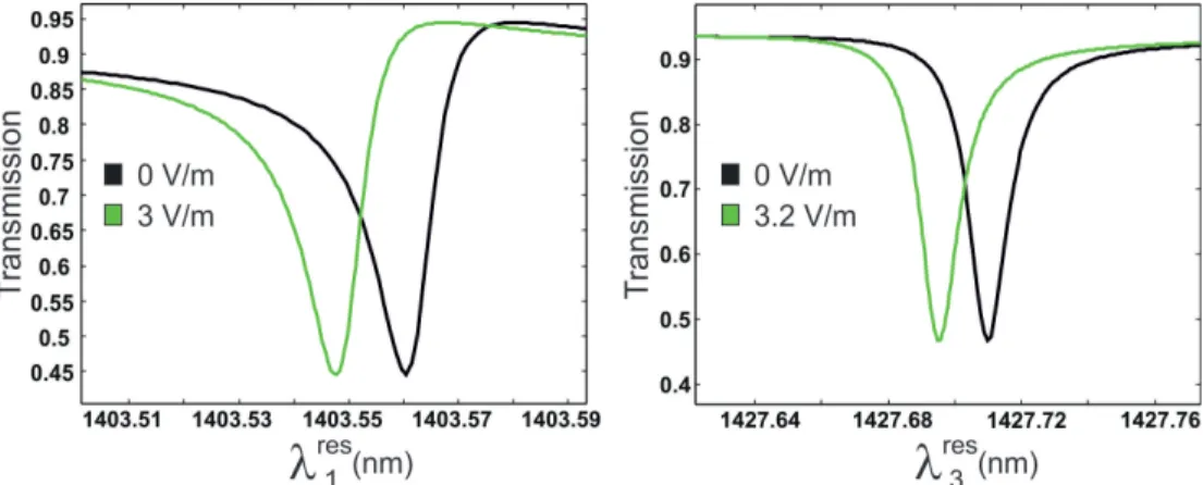
Fig. 5. Transmission spectra for the resonance λr es 1 and λ
r es
3 for the free structure (black lines) and when external E-fields are applied (green lines) with Es= 3 V/m and Es= 3.2 V/m.
To estimate this sensitivity, we perform numerical simulations in three steps: (a) The structure is first assumed to be free from any external E-field meaning that LN has a homogeneous refractive optical index and we calculate the transmission spectrum. (b) From the latter we perform a second FDTD numerical simulation in CW regime at λ= λr esto estimate, cell by
cell, the optical field factor given by Eq. 4. (c) In the last step, after injecting these fop(x, y, z)
values into Eq. 3, we carry out a new FDTD-simulation taking into account the modification of the refractive optical index of each FDTD cell and determine the transmission spectrum in the presence of an external E-field Eswhose value is fixed.
As a result, an E-field of around 3 V/m is required to tune over a spectral range of width 11.9 pm corresponding to the FWHM of the resonance at λr es1 and Es= 3.2 V/m for λr es3 over
14.0 pm as shown in Fig. 5. Experimentally, this shift is sufficient to be detected through the measurement of the transmission spectrum using a common low-price Optical Spectrum Analyzer (OSA) (such as MS9710B from Anritsu, which has a read resolution of 5 pm1 ). Thus, if an Optical Spectrum Analyzer (OSA) with a high resolution of 0.1 pm is employed (such as the BOSA 100 from Aragon Photonics which has an optical resolution of 0.08 pm/10 MHz 2), we estimate to 25 µV/m the minimum detected electric field.
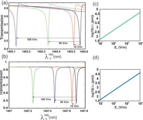
Fig. 6 shows the different spectra for different external E-field values (0, 10 V/m, 50 V/m, 100 V/m) for the two resonances λr es
1 in (a) and λ r es
3 in (b). For both cases, we plot on Figs 6(c) and
(d) the shift of the resonance as a function of the external E-field. As expected, the two behaviors are linear with quite similar slope values corresponding to the sensitivity of the configuration which is equal to S = 4 pm.m/V. Let us note that this sensitivity is more than 160000 times greater than the one obtained in ref. [22] (see Fig. 3(a) of that paper) where a shift of 7 pm/V is announced for electrodes separated by a gap of 3.5 µm (electric field of almost 286 kV/m).
4. Conclusion
In conclusion, we have designed and numerically studied by home-made FDTD codes the excitation of ultra-high Q-factor resonances up to 1.2 × 10⁶ associated with the excitation of
SPMs which are excited assuming an illumination with a small angle of incidence θ = 0.5◦.
1http://www.smart-inc.com.tw/uploads/root/MS9710B_E1700.pdf
2https://www.gophotonics.com/products/optical-spectrum-analyzers/ aragon-photonics/58-667-bosa-100
Fig. 6. The spectral position shift of (a)λr es1and (b)λr es3as function of the external E-field Es. The variation of the spectral shift of (c)λr es1 and (d)λr es3 versus the applied electric field. It shows a linear behavior.
Furthermore, by exploiting such sharp resonances, we can develop an E-field sensor with a sensitivity of 4 pm.m/V. It results from a local confinement of the electromagnetic field reaching a local optical field factor up to 245. This kind of hybrid Fano-symmetry protected modes opens the way to a new generation of sensors assuming good quality manufacturing processes able to guarantee a high degree of symmetry of the fabricated structure. External E-fields as small as 25 mV/m can then be detected with such device, making it possible to be used for medical investigations such as ECG.
Disclosures
The authors declare no conflicts of interest. Add references with BibTeX or manually.
References
1. V. Calero, M.-A. Suarez, R. Salut, F. Baida, A. Caspar, F. Behague, N. Courjal, L. Galtier, L. Gillette, L. Duvillaret, G. Gaborit, and M.-P. Bernal,"An ulta wideband-high spatial resolution-compact electric field sensor based on lab-in-fiber technology," Sci. Rep. 3(1), 8058 (2019).
2. A. E Cetin, and S. N. Topakaya, "Photonic crystal and plasmonic nanohole based label-free biodetection," Biosens. Bioelec. 132, 196–202 (2019).
3. K. Saker, T. Bouchemat, M. Lahoubi, M. Bouchemat, S. Pu, "Magnetic field sensor based on a magnetic-fluid-infiltrated photonic crystal L4 nanocavity and broadband W1 waveguide," J. Comp. Elec. 18(2), 619–627 (2019).
4. G. Wang, Y. Lu, X. Yang, L. Duan, J. Yao, "Square-lattice alcohol-filled photonic crystal fiber temperature sensor based on a Sagnac interferometer," Appl. Opt. 58(8), 2132–2136 (2019).
5. V. Arumuru, J. N. Dash, D. Dora, and R. Jha. "Vortex shedding optical Flowmeter based on photonic Crystal Fiber," Sci. reports,9(1), 1–9 (2019).
6. W. Qiu, et al. "Fano resonance-based highly sensitive, compact temperature sensor on thin film lithium niobate," Opt. Lett. 41(6), 1106–1109 (2016).
7. T. SÃijnner, T. Stichel, S. H. Known, T. W. Schlereth, S. HÃűfling, M. Kamp, and A. Forchel, "Photonic crystal cavity based gas sensor," Appl. Phys. Lett. 92(26), 261112 (2008).
8. Y. Liu, S. Wang, P. Biswas, P. Palit, W. Zhou, Y. Sun, "Optofluidic vapor sensing with free-space coupled 2D photonic crystal slabs," Sci. Rep. 9(1), 4209 (2019).
9. S. Obeid, A. Ceroi, G. Mourey, P. Saas, C. Elie-Caille, W. Boireau, "Development of a NanoBioAnalytical platform for on-chip qualification and quantification of platelet-derived microparticles," Biosen. Bioelec. 93, 250–259 (2017). 10. Y. Zhou, X. Li, S. Li, Z. Guo, P. Zeng, J. He, D. Wang, R. Zhang, M. Lu, S. Zhang, and X. Wu, "Symmetric guided-mode resonance sensors in aqueous media with ultrahigh figure of merit," Opt. Express 27(24), 34788-34802 (2019).
11. H. Zhang, D. Peng, W. Wang, L. Dong, and C. Pan, "Mechanically induced light emission and infrared-laser-induced upconversion in the Er-doped CaZnOS multifunctional piezoelectric semiconductor for optical pressure and temperature sensing," J. Phys. Chem. C 119(50), 28136–28142 (2015).
12. S. Kostritskii, M. Aillerie, E. Kokanyan, and O. Sevostyanov, "Parameters of nonlinear scattering evaluated by open-aperture Z-scan technique in photorefractive Li N bO3crystals" Opt. Quant. Electron., 52(2), 92 (2020). 13. E. H. Putley, "Indium antimonide submillimeter photoconductive detectors," Appl. Opt. , 4(6), 649–657 (1965). 14. E. M. Logothetis, H. Holloway, A. J. Varga, and W. J. Johnson, "nâĂŘp junction ir detectors made by proton
bombardment of epitaxial PbTe," Appl. Phys. Lett. , 21(9), 411–413 (1972).
15. Z. Wang, R. Yu, X. Wang, W. Wu, and Z. L. Wang, "Ultrafast response pâĂŘSi/nâĂŘZnO heterojunction ultraviolet detector based on pyroâĂŘphototronic effec," Adv. Mat., 28(32), 6880–6886 (2016).
16. H. Wang, R. Zeng, and C. Zhuang, "Thermal variation of electric field sensor bias caused by anisotropy of LiNbO3," Appl. Phys. Lett. 114(14), 143501 (2019).
17. R. Zeng, C. Zhuang, Z. Yu, Z. Li, and Y. Geng, "Electric field step in air gap streamer discharges," Appl. Phys. Lett. 99(22), 221503 (2011).
18. O. Ogawa, T. Sowa, and S. Ichizono, "A guided-wave optical electric field sensor with improved temperature stability," J. Light. Techn. 17(5), 823 (1999).
19. J. M. Lourtioz, H. Benisty, V. Berger, J. M. Gerard, D. Maystre, and A. Tchelnokov, "Photonic crystals," Towards Nanoscale Photonic Devices (2005).
20. M. Roussey, M.-P. Bernal, N. Courjal, and F. I. Baida, "Experimental and theoretical characterization of a lithium niobate photonic crystal," Appl. Phys. Lett. 87(24), 241101 (2005).
21. W. Qiu, A. Ndao, H. Lu, M.-P. Bernal, and F. I. Baida, "Guided resonances on lithium niobate for extremely small electric field detection investigated by accurate sensitivity analysis," Opt. Express 24(18), 20196–20209 (2016). 22. C. Wang, M. Zhang, B. Stern, M. Lipson, and M. LonÄŊar, "Nanophotonic lithium niobate electro-optic modulators,"
Opt. Express 26(2), 1547–1555 (2018).
23. R. S. Weis, and T.K. Gaylord, "Lithium niobate: summary of physical properties and crystal structure," Appl. Phys. A 37(4), 191–203 (1985).
24. A. Guarino, A. Guarino, G. Poberaj, D. Rezzonico, R. Degl’Innocenti, and P. GÃijnter, "Electro-optically tunable microring resonators in lithium niobate," Nature Photon. 1(7), 407 (2007).
25. K. K. Wong, "Properties of lithium niobate," (28) IET, (2002).
26. R. El-Ganaini, K. G. Makris, M. Khajavikhan, Z. H. Musslimani, S. Rotter, and D. N. Christodoulides, "Non-Hermitian physics and PT symmetry," Nature Phys. 14(1), 11 (2018).
27. L. Lu, C. Fang, L. Fu, S. G. Johnson, J. D. Joannopoulos, and M. SoljaÄŊiÄĞ, "Symmetry-protected topological photonic crystal in three dimensions," Nature Phys. 12(4), 337 (2016).
28. J. W. Yoon, . H. Song, and R. Magnusson, "Critical field enhancement of asymptotic optical bound states in the continuum," Scien. Rep. 5, 18301 (2015).
29. W. Zhang, B. Gallinet, and O. J. Martin, "Symmetry and selection rules for localized surface plasmon resonances in nanostructures," Phys. Rev. B 81(23), 233407 (2010).
30. S. Campione, S. Liu, L. I. Basilio, L. K. Warne, W. L. Langston, T. S. Luk, J. R. Wendt, J. L. Reno, G. A. Keeler, I. Brener, and M. B. Sinclair, "Broken symmetry dielectric resonators for high quality factor Fano metasurfaces," Acs Photonics, 3(12), 2362–2367 (2016).
31. J. Lee, B. Zhen, S. L. Chua, W. Qiu, J. D. Joannopoulos, M. SoljaÄŊiÄĞ, and O. Shapira, "Observation and differentiation of unique high-Q optical resonances near zero wave vector in macroscopic photonic crystal slabs," Phys. Rev. Lett. 109(6), 067401 (2012).
32. A. Kodigala, T. Lepetit, Q. Gu, B. Bahari, Y. Fainman, and B. KantÃľ, (2017)"Lasing action from photonic bound states in continuum," Nature 541(7636), 196 (2017).
33. B. Gallinet, T. Siegfried, H. Sigg, P. Nordlander, and O. J. Martin, "Plasmonic radiance: probing structure at the angstrom scale with visible light," Nano. Lett. 13(2), 497–503 (2013).
34. G. Ulliac, B. Guichardaz, J. Y. Rauch, S. Queste, S. Benchabane, and N. Courjal, "Ultra-smooth LiNbO3 micro and nano structures for photonic applications," Microelec. Eng. 88(8), 2417–2419 (2011).
35. M. Roussey, F. I. Baida, and M. P. Bernal, "Experimental and theoretical observations of the slow-light effect on a tunable photonic crystal," JOSA B, 24(6), 1416–1422 (2007).
ed. Artech House, Norwood, MA, 2005.
37. A. Hoblos, M. Suarez, B. Guichardaz, N. Courjal, M. P. Bernal, F. I. Baida, "Revealing photonic Symmetry-Protected Modes by Finite-Difference-Time-Domaine method," Opt. Lett. 45(7), 2103–2106 (2020).
38. A. Ndao, R. Salut, M. Suarez, and F. I. Baida, "Plasmonless polarization-selective metasurfaces in the visible range," J. Opt. 20(4), 045003 (2017).
39. A. Belkhir, and F. I. Baida, "Three-dimensional finite-difference time-domain algorithm for oblique incidence with adaptation of perfectly matched layers and nonuniform meshing: Application to the study of a radar dome," Phys. Rev. E,77(5), 056701 (2008).
40. C. Blin, X. Checoury, H. A. Girard, C. Gesset, S. Saada, P. Boucaud, P. Bergonzo, "Optical Analysis of p-Type Surface Conductivity in Diamond with Slotted Photonic Crystals," Adv. Opt. Mat. 1(12), 963–970 (2013).