Science Arts & Métiers (SAM)
is an open access repository that collects the work of Arts et Métiers Institute of Technology researchers and makes it freely available over the web where possible.
This is an author-deposited version published in: https://sam.ensam.eu Handle ID: .http://hdl.handle.net/10985/18495
To cite this version :
M.G. TSOUTSOUVA, T. RIBERI – BÉRIDOT, G. REGULA, G. REINHART, J. BARUCHEL, Fabrice GUITTONNEAU, Laurent BARRALLIER, N. MANGELINCK-NOËL - In situ investigation of the structural defect generation and evolution during the directional solidification of 110 seeded growth Si - Acta Materialia - Vol. 115, p.210-223 - 2016
In situ investigation of the structural defect generation and evolution during the
directional solidification of <110> seeded growth Si
M.G. Tsoutsouva(a), T. Riberi – Béridot(a), G. Regula(a), G. Reinhart(a), J. Baruchel(b), F. Guittonneau(c), L. Barrallier(c), N. Mangelinck-Noël(a)*
(a)Aix-Marseille Université, CNRS, IM2NP UMR CNRS 7334, Campus Saint Jérôme, case 142,
13397 Marseille Cedex 20, France.
(b)ESRF, 71, avenue des Martyrs, CS40220, 38043 Grenoble Cedex 9, France.
(c)ARTS ET METIERS PARISTECH/INSTITUT CARNOT ARTS CENTRE AIX-EN-PROVENCE
2, cours des Arts et Métiers.13617 Aix-en-Provence, cedex 1, France.
*Corresponding author: Dr. N. Mangelinck-Noël
Aix-Marseille Université, CNRS, IM2NP UMR CNRS 7334, Campus Saint Jérôme, case 142, 13397 Marseille Cedex 20, France
telephone : + 33 (0) 4 91 28 87 37 fax: +33 (0) 4 91 28 87 75
In situ investigation of the structural defect generation and evolution during the
directional solidification of <110> seeded growth Si
M.G. Tsoutsouva(a), T. Riberi – Béridot(a), G. Regula(a), G. Reinhart(a), J. Baruchel(b), F. Guittonneau(c), L. Barrallier(c), N. Mangelinck-Noël(a)*
(a)Aix-Marseille Université, CNRS, IM2NP UMR CNRS 7334, Campus Saint Jérôme, case 142,
13397 Marseille Cedex 20, France.
(b)ESRF, 71, avenue des Martyrs, CS40220, 38043 Grenoble Cedex 9, France.
(c)ARTS ET METIERS PARISTECH/INSTITUT CARNOT ARTS CENTRE AIX-EN-PROVENCE
2, cours des Arts et Métiers.13617 Aix-en-Provence, cedex 1, France.
Abstract
This work is dedicated to the advanced in situ X-ray imaging and complementary ex situ investigations of the growth mechanisms when silicon solidifies on a monocrystalline seed oriented <110> in the solidification direction. It aims at deepening the fundamental understanding of the phenomena that occur throughout silicon crystal growth with a particular focus on mechanisms of formation of defects detrimental for photovoltaic applications. Namely, grain nucleation, grain boundary formation and evolution, grain competition, twining occurrence, dislocation generation and interaction with structural defects are explored and analysed. Nucleation of twin crystals preferentially occurs on {111} facets at the edge of the sample where solid – liquid – vapor triple point lines exist in interaction also with the crucible as well as, at grain boundary grooves at the solid – liquid interface (solid – solid – liquid triple lines), where two grains are in competition, either on the {111} facets of the groove or in the
groove. Enhanced undercooling and/or stress accumulation levels are found to act as driving forces for grain nucleation. Additionally, it is demonstrated that twin formation has the property to relax stresses stored in the crystal during the growth process. However, grains formed initially in twin position can undergo severe distortion when they are in direct competition or when they are squeezed in – between grains. Moreover, we show by X-ray Bragg diffraction imaging that on the one hand, coherent Σ3 <111> grain boundaries efficiently block the propagation of growth dislocations during the solidification process, while on the other hand, dislocations are emitted at the level of incoherent and / or asymmetric Σ27a <110> at the encounter with either Σ3 <111> or Σ9 <110> grain boundaries. Indeed, grain boundaries that deviate from the ideal coincidence orientation act as dislocation sources that spread inside the surrounding crystals.
Keywords: X-ray diffraction imaging, X-ray radiography, twinning, grain competition, dislocations, structural defects
1 Introduction
Aiming to the production of low cost and high efficiency silicon based solar cells for photovoltaic (PV) applications, current research focuses on several key targets such as the optimization of silicon growth processes and the improvement of the crystalline quality of the final ingot. With the conventional multicrystalline silicon (mc-Si) growth technique, the silicon structure cannot be controlled at all. Three alternative technologies have been proposed to master the initial grain nucleation and defect generation at the bottom of the crucible during the first stage of solidification: the dendritic casting method, the mono-like solidification (ML-Si) and the high performance multi-crystalline silicon (HP mc-Si). A major issue shared by all techniques is to control and lower the density of dislocations. Indeed, it is well known that
dislocations have a strong harmful effect on the efficiency of solar cells, because they can act as preferential segregation sites for impurities ultimately reducing the carrier lifetime.
Recently, Fujiwara et al. presented the dendritic casting method as a new concept to tailor the grain orientation and grain size by controlling the undercooling of the initial grown melt [1]. The ultimate goal of this technique is to obtain an ingot with large grains, low density of random grain boundaries and thus lower density of dislocations. However, the control of the undercooling is not easy in a commercial growth facility due to the large thermal resistance from the thick bottom of the silica crucible and of the imperfect Si3N4 coating of the crucible
walls [2,3].
The simplest way to control the grain structure formation is to use seeds at the bottom of the crucible. Two approaches have been reported in the literature, which represent the two extreme grain configurations; the Si and the HP mc-Si. On the one hand, in the case of ML-Si, a pavement of monocrystalline seeds is placed on the bottom of the crucible in order to grow a mono-crystalline ingot, taking up the initial orientation of the seed [4]. However, ML-Si efficiencies are still limited due to the presence of structural defects such as parasitic grain nucleation on the walls of the crucible [5,6], twin formation and dislocations. The latter, can be either arranged in cellular patterns, in the entire mono-like Si ingot and are known as background dislocations [7] or generated on the top of the seeds [6,8], at their junctions [6,9– 12], on precipitates and subsequently propagate vertically along the growth direction [4,5,13,14] inducing the formation of sub-grain boundaries. On the other hand, the ultimate goal of the HP mc-Si technique is to obtain small and uniform grains at the initial stage of solidification with random angle and coherent grain boundaries. This would result in low density of dislocation clusters thanks to the interaction of blocking mechanisms by which dislocations that nucleate at the beginning of the crystallization process cannot propagate further along the growth of the ingot. In the literature, chips [15] (small Si pieces) and granules
[16,17] (small spherical Si beads) have been reported to be used as seeds for HP mc-Si ingot growth with promising results. However, from the work presented on the literature, we can conclude that it is essential to better understand and control the initial grain size and orientation distribution at both bottom and walls of the crucible, as well as the initial defect density to obtain the targeted dislocation density reduction higher in the ingot [18].
Both ML-Si and HP mc-Si techniques have a lower defect density than the conventional mc-Si while allowing the use of low-cost casting solidification methods [19]. However, as seen above, there still exist huge and inherent challenges related to: the control of the initial grain nucleation, twinning frequency occurrence, grain competition, defect generation, their interaction with grain boundaries and their evolution during growth. As a conclusion, further research is needed to increase the competitiveness of those processes and to reach an efficient mass production. Few works are available in the literature discussing those phenomena stepping forward possible grain formation, grain boundary interaction and dislocation generation mechanisms [20–25]. Nevertheless, current fundamental research progress is limited by the difficulty of accessing, from the ex situ study of the solidified ingots, understanding and control of the processes occurring during crystallization.
This paper is devoted to the mechanisms involved in the crystallization process that must be first understood to be controlled in a further step. Advanced in situ and complementary ex
situ characterisation methods are used to investigate Si growth mechanisms when Si is
solidified from a Si seed oriented <110> in the solidification direction. We focus on the grain nucleation, the grain boundary formation, the grain competition, the twining occurrence, the dislocation generation and interaction with either themselves and/or structural defects, aiming at deepening the fundamental understanding on the phenomena that occur during the Si crystal growth.
2 Experimental procedure
2.1 In situ X-ray imaging during crystal growth
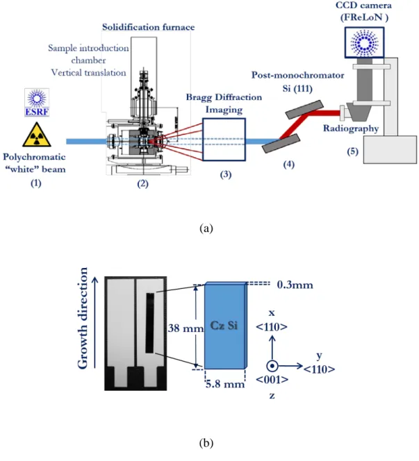
GaTSBI (Growth at high Temperature observed by Synchrotron Beam Imaging) is a unique device for Si that allows following in real time its solidification process during growth. It is a specially designed instrument composed of a high temperature directional solidification (DS) furnace employed in conjunction with synchrotron radiation X-ray imaging techniques (Bragg diffraction imaging and radiography). GaTSBI not only provides information on the solid – liquid interface dynamics, but also gives access to the single grain dynamic evolution during growth, the crystalline orientation / misorientation, the qualitative level of local distortion, the nature of structural defects, as well as the low angle grain boundaries in single crystalline materials. A detailed description of the equipment, of the imaging techniques and of the previously obtained results can be found elsewhere [26–29].
Solidification experiments are carried out at beam line BM05 at the European Synchrotron Radiation Facility (ESRF) and a schematic illustration of the experimental installation is presented in Fig.1. The directional furnace is based on two resistive heating elements (top and bottom). A Cz silicon sample, housed in a BN crucible (Fig.1b), is introduced inside the DS furnace. The front and back sides of the sample (38 mm × 5.8 mm × 0.3 mm) are in contact with the crucible walls (Fig. 1b). Solidification experiments are performed in high vacuum (~10-6 mbar) under a constant temperature gradient, G=30 K/cm, imposed between the
two heating resistances. Directional solidification of the remaining liquid is obtained by applying a cooling rate R on both heaters in the range of 0.2 – 4 K/min. Several melting/solidification cycles are carried out with the same sample. Initially, the sample is partially melted to be able to initiate growth from the seedthen, the crystal is solidified taking up the initial orientations of the seed (Fig.1b).
The polychromatic synchrotron radiation (Fig.1a.(1)) illuminates the Si sample during the whole crystal growth process. X-ray Bragg diffracted beams, corresponding to different hkl diffracting planes, are regularly recorded on X – ray sensitive films (AGFA Structurix D3-SC, 17.6×12.5 cm2) positioned at a distance of 300 mm from the sample (Fig.1a.(3)). Due to the
small beam divergence and its large size, the whole width of the sample is illuminated and the recorded Bragg diffraction images contain information on the individual grain shape, misorientation and deformation level. This is a powerful technique that can be used for the visualization of defects (dislocations, twins, domain walls, inclusions, impurity distribution) present in the crystal volume. Indeed, it records their long range distortion fields and / or the strain fields associated with a macroscopic crystal deformation. This is made possible, because these distortion fields affect the diffracted intensity, so that a contrast (non – homogeneous intensity distribution) is created in the recorded image. In this way, Bragg diffraction imaging can also be explained as a study of the fine structure of a Bragg spot which contains information about the deviation from the perfect crystal structure.
In the second mode (X – ray radiography), the polychromatic beam, after passing through the sample, is monochromated at 17.5 keV using a vertically diffracting Si (111) double-crystal monochromator (Fig.1a.(4)). The X – ray radiography images are recorded using a specific CCD camera developed at the ESRF named FReLoN (Fast Readout Low-Noise) [30] with 2048×2048 image pixel size (Fig.1a.(5)). In the present experiment, an optics giving a 5.8 μm pixel size and a 11.9 × 11.9 mm2 field of view is used. The X – ray radiography images obtained are absorption contrast images. However, the absorption coefficient of the solid and liquid Si depends on their mass densities which are not much different (2.31 g/cm3 for the solid and 2.56 g/cm3 for the liquid) meaning that the solid / liquid interface in the raw images is hardly distinguishable. As a consequence, an image processing method consisting of successive images division is applied to reveal the shape of the solid / liquid interface more accurately
[26]. Both imaging techniques provide complementary dynamic information about crystal growth and competition.
2.2 Ex situ complementary investigations
After the last melting – solidification cycle, the sample is removed from the GaTSBI furnace and mirror polished down to a 1 μm diamond paste. It is then characterised ex situ by Synchrotron X – ray rocking curve imaging (RCI) which is a quantitative version of monochromatic beam X – ray Bragg diffraction imaging [31–34]. The experiments are carried out at beamline BM05 at the ESRF as well. The synchrotron radiation is monochromated at 20 keV using a vertically diffracting Si (111) double-crystal monochromator. The sample is positioned to diffract the Si {220} reflection in the vertical scattering plane (the Bragg angle (θB) for Si {220} at 20 keV is 9.28°). The crystal is rotated along the diffraction curve for the
Si {220}, and the diffracted beam profile is recorded on a CCD camera equipped with an optic of 10 μm per pixel and 20.5 × 20.5 mm2 field of view. The series of rocking curve images are
recorded during sample rotation (ω – scan) with angular steps of 0.0005° over a range of 0.15° across the Bragg angle. Each pixel of the camera records its own local rocking curve, so that maps of the whole diffracting area of the sample can be reconstructed. Maps of integrated intensity and full width at half maximum (FWHM) give information about the level of local distortion in each zone of the crystal, and maps of the angular peak position give access to the local deviation from the theoretical Bragg angle. Several previous studies [11,12,35,36] have proved that RCI using synchrotron light, which provides a high angular resolution (<10-4 °), is a powerful tool for visualizing and measuring the lattice distortion and deformation in single – crystalline materials.
Additionally, electron backscatter diffraction (EBSD) scans are executed on a FEG-SEM JEOL JSM 7001F equipped with a HKL Nordlys camera using either a 7 μm or a 0.7 μm step size. In order to extract the three – dimensional orientation of the sample, color code orientation
maps (inverse pole figures (IPF)) are generated with respect to the directions perpendicular to the sample surface (y, z) and in the growth direction (x). Coincidence site lattice maps (CSL) are reconstructed to evidence the boundaries with a special character. In this paper, Σ3 <111>, Σ9 <110>, Σ27a <110>, Σ27b <210> twin boundaries labeling refer to rotations around <h k l> that satisfy the misorientation ranges given by the Brandon criterion, which are (60 ± 8.66)°, (38,94 ± 5)°, (31.58 ± 2.89)° and (35.42 ± 2.89)°, respectively. The character (symmetric or asymmetric) of the grain boundary, the orientation of the crystallographic planes of the adjacent grains and the deviations from the optimum crystallographic orientation are identified by a detailed analysis of the stereographic projections of the appropriate crystallographic planes. Assessment of lattice strain distribution is conducted by the local misorientation approach. This method assumes that strain – induced dislocation structure development is associated with rotation of “micro – volumes” (cells, sub-grains) leading to an increase of local variations in lattice orientation (misorientation) between adjacent points. There are few metrics that may be used for quantitative analysis in this approach [37]. In this work, two of them have been selected: i) the grain orientation spread (GOS) map that measures the difference between the orientation of every pixel in the grain and the grain average orientation, to put in evidence the more distorted grains and ii) the average local misorientation (LMP) map to locate deformed regions inside grains. This component shows the average local misorientation for misorientations below the sub-grain boundary angle (< 5°) using a filter size 3 × 3 pixels.
3 Experimental results
As revealed from the X-ray radiography experiments and also observed in our previous work [27], for all the imposed cooling rates (0.2 – 4 K/min), the solid / liquid interface remains smooth and quasi planar during the solidification of Cz silicon. Fig. 2 presents the EBSD crystallographic orientation maps (IPF) of the lastly solidified sample (13th melting
with {101} parallel (x) and perpendicular (y) to the growth direction, {001} being perpendicular to the surface of the sample (z). However, parasitic grain nucleation occurs at both sides of the sample where solid – liquid – vapour – crucible point lines (SLVC – PL) are present. Those grains come in competition with the two elongated grains that grow vertically on the left and right side of the central grain from the seed, and their lateral growth is prevented. No grain competition takes place between the two vertical grains and the central main grain during growth.
Horizontal successive twinning revealed by the alternation of two crystallographic orientations occurs at the left side of the sample. As demonstrated by the coincidence site lattice (CSL) map (Fig. 3a) and the crystallographic orientation (Fig. 2) map, all those twins are in a Σ3 <111> relation between them and their crystallographic orientations alternate between the initial orientation of the seed ([1�1�0] along x, [11�0] along y, [001] along z) and an orientation that corresponds to [41�1�] along x, [011�] along y and [122] along z.
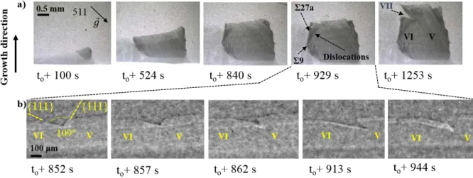
The white beam X-ray Bragg diffraction images taken during the solidification process (Fig. 4a), illustrate that the parasitic twin nucleation initially occurs at the edge of the sample at the SLVC – PL. Each formed twin crystal grows vertically and laterally towards the centre of the sample where it becomes in competition with the vertically grown crystal, leading to the formation of a distorted Σ27a <110> grain boundary (shown by a dotted arrow in Fig. 4a). As it will be discussed later in this paper, this Σ27a <110> grain boundary corresponds to a 3rd order symmetrical Σ27a <110> / {511}1,2, which is the most densly packed plane in the CSL,
at the beginning of its formation and very quickly during growth it evolves to a 3rd order symmetrical Σ27a <110> / {552}1,2 grain boundary, which correspond to a less densed pack
plane in the CSL. Fig. 4b presents the X-ray radiography images revealing the nucleation and growth of one of the successive twins between to+405 s and to+466 s. It is important to note that
corresponds to a liquid layer in the previous image that has been solidified in the following one. On the right side of the same figure, the groove that is formed due to the grain competition between the horizontal twin and the vertically grown grain leading to the formation of the distorted Σ27a <110> grain boundary is also evidenced (dotted arrow).
Similarly to the left side of the sample, on the right side horizontal twin nucleation occurs at the edge of the sample (SLVC – PL) (Fig. 5a). As described previously, in a similar way, the grain V grows vertically and laterally on the {111} facet and it becomes in competition with the vertically growing grain from the seed in the central part of the sample. A Σ3 <111> grain boundary is formed between those two grains until the moment that the nucleation of grain VI happens (position ζ in Fig. 3a) leading to the formation of a Σ9 <110> grain boundary. As the growth proceeds, at the encounter of the Σ9 <110> with the vertically grown coherent Σ3 <111> grain boundary, a successive vertical twin nucleation in a Σ3 relation occurs leading to the formation of a Σ27a <110> grain boundary (position β in Fig. 3a). Those vertical twins propagate along the growth direction and they are efficiently blocked by a diagonal Σ3 <111> twin boundary higher in the sample (position δ in Fig. 3a). From the corresponding white beam Bragg diffraction images (Fig. 5a), it can be seen that the Σ27a <110> grain boundary is highly distorted, dislocations are emitted (position β in Fig. 3a) and propagate inside grain VI, while the surrounding area of the position β appears to be two times more distorted in comparison to the average level of distortion of the sample (position β in Fig. 3b).
Grain VI is in a Σ3 <111> twin relation with grain V and it finally takes over grain V during growth. As revealed by the X – ray radiography images (Fig. 5b), a facetted / facetted groove is formed at the solid-liquid interface due to the competition between grains V and VI (position ε in Fig. 3a). Then, grain nucleation occurs on the {111} left facet (Fig. 5b) leading to the formation of a twin crystal that blocks the further growth of grain VI. In parallel, grain nucleation also takes place on the right {111} facet leading to the formation of a Σ9 <110> and
a Σ27a <110> grain boundary. From this point, the growth direction changes and grain V is free to occupy the space.
The main difference between the twin nucleation at the edge of the sample on the left and on the right side is that in the last case, successive horizontal twinning does not occur. Indeed, a first horizontal twin crystal nucleates and grows with the same crystallographic orientation as the first nucleated successive twin on the left side. Later in the growth, instead of horizontal successive twinning (left side of the sample), diagonal successive twining at the edge of the sample is observed and evidenced by the alternation of two crystallographic orientations. Fig. 6 shows snapshots of the successive twin nucleation on the corresponding diagonal {111} facet at the right edge of the sample as observed in dynamic by X – ray radiography.
As shown in the CSL map (Fig 3.a), most of the grains in the sample are in twin relationship and the Σ3 <111> grain boundary is the dominant CSL type. The dynamic information obtained from the in situ imaging proves that higher order twin grain boundaries, Σ9 <110> are formed at the encounter of two grains that previously nucleated with a Σ3 <111> relation on the same grain. Σ27a <110> grain boundaries are formed between two grains that are in a Σ3 <111> twin relation with other grains [28]. All the horizontal and diagonal twin boundaries initiating at the edge of the sample are a Σ3 <111> type. Only coherent Σ3 <111> twins have been identified as growth twins. Incoherent Σ3 <111> and higher order twin boundaries (Σ9 <110> and Σ27a <110>) are the result of grain encounter and competition.
Fig.3b shows the rocking curve imaging (RCI) integrated intensity map of the Si (220) reflection that gives a quantitative information about the level of distortion in the sample. There is a clear relation between the local distortion and the formed grain boundary type (Fig. 3a positions α, β and γ). Indeed, zones where Σ27a <110> grain boundaries are present, are two times more distorted in comparison to the average distortion of the whole sample. Moreover, the Σ3 <111> vertical grain boundary on the right side of the sample becomes more distorted
after the encounter with a Σ27a <110> grain boundary (Fig. 3b position γ). In a subsequent step of growth, it is relaxed after the encounter with a diagonal Σ3 <111> twin boundary (Fig. 3b position δ). The right part of the sample does not appear in Fig.3b since it is out of Bragg angle diffraction. The grain orientation spread map (GOS) obtained from the EBSD measurements (Fig. 3c) is a representative image of the level of distortion of each grain and it is in accordance with the RCI map. Moreover, it can be seen that successive twins are less distorted in comparison to the seed and the up grown crystal. Consequently, the twin crystals have smaller level of distortion and thus a lower dislocation density in comparison to the seed. Additionally, from the same figure it becomes obvious that grains that underwent competition with other grains during the solidification process present the highest level of distortion (see grains appearing in red and orange colors in Fig. 3c).
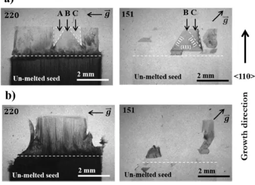
Fig. 7 shows the Bragg diffraction images of the Si (2�2�0) and (151) that correspond to the first (Fig. 7a) and the fifth (Fig. 7b) melting / solidification cycles of the same sample. Dark zones represent strain fields associated to the presence of structural defects. The fact that the un – melted seed appears dark, is mainly due to the solid state reaction between the BN crucible and the Si sample, leading to the formation of a Si3N4 layer on the surface of the un – melted
seed. It is observed that the diffraction images become darker when increasing the melting / solidification number of cycles due to the accumulation of the above mentioned phenomenon, denoting the degradation of the crystalline quality of the seed. After cooling down, the diffraction images are more deformed as observed when performing ex situ Bragg diffraction and RCI measurements, this is due to the additional thermal induced residual stresses which arise during the cooling process. The effect of cooling down to the ambient temperature on the generation and evolution of already present and additional defects in the solidified Si will not be discussed in the present paper. Further in situ investigations are currently ongoing to obtain more accurate results that will be presented in an upcoming publication. In Fig. 7a, twinning
occurrence (big triangular central crystal (grain B)) and two upside down squared – triangular grains on their sides (grains A and C) can be observed in the centre of the up-grown crystal. The fact that grain B diffracts together with the seed crystal on the (2�2�0) diffraction image and alone elsewhere on the X- ray sensitive film ((151) diffraction image of the seed) denotes that it is in twin position with the seed. From the same figure, it can also be observed that grains A and C do not diffract at all in the (2�2�0) diffraction image with the seed, while grain C diffracts in the (151) diffraction spot of the seed with grain B. This is the indication that those grains are in different twin relationships between them and with the other grains of the up-grown crystal. Dislocations originating in the seed propagate vertically in the up-grown crystal along the <110> growth direction during the solidification process. However, their propagation is efficiently blocked by the formation of the horizontal twin boundary (between the up – grown crystal and the grain B) since they are no longer visible in the inner part of the twin crystal B (Fig. 7a). However, when this twin related blocking mechanism is not present, dislocations propagate along the whole height of the up-grown crystal. A representative case of this phenomenon can be seen in Fig. 7b that corresponds to the fifth melting / solidification cycle of the sample. Dislocations are observed, as straight dark lines in the (2�2�0) diffraction image and they develop upwards being aligned along the <110> growth direction. In this case, no twinning event occurs in the central part of the sample, as confirmed by the (151) diffraction image.
All twin crystals (A, B and C) are of high crystallographic quality and no distorted areas are observed in their volume. The zones at the facet junctions, where the nucleation of grains A and B occurs, are highly distorted and act as sources for the generation of dislocations that spread in the interior part of the surrounding crystals (Fig. 7a). A vertical distorted grain boundary is formed at the right side of grain C, at the junction with the grain growing on the seed, while no distortion is observed at the grain boundary formed between grains B and C.
4 Discussion
As described in the previous section, during growth twinning, grain competition and defect generation occur determining the final structure of the solidified sample. In the following, it will be shown that all those events and involved mechanisms tend to reduce the total energy of the system. The three main phenomena are discussed in details: i) the twin nucleation mechanisms at the edge of the sample; ii) the grain competition and the related deformation; iii) the generation of dislocations and their interaction with grain boundaries.
4.1 Twin nucleation at the border of the sample (solid – liquid – vapor and / or crucible phase lines (SLV/C– PL)
During the solidification of silicon, twin nucleation is commonly observed at the edge of the ingot. The nucleation can be explained by the model proposed by Voronkov and Hurle [38,39] which is based on the formation of twins on {111} facets. They suggest that twinning can happen when (i) an edge facet is attached to the SLV/C – PL, (ii) the external surface of the growing crystal is oriented such that the formation of a twinned nucleus produces a segment of {111} oriented surface and (iii) the undercooling at the edge of the facet exceeds a critical value. Twin nucleation in the bulk crystal is thermodynamically unfavorable and in the case of silicon is always related to the presence of {111} facets at the solid liquid interface [40]. Since twinning requires a high undercooling in order to occur in the middle of a facet, it is usually observed at a solid – liquid – grain boundary triple line (SSL - TL) in the case of multi – crystalline silicon solidification [29,41], at the solid – liquid – vapour triple lines (SLV – TL) in the case of Czochralski growth [38,39] and at the borders, where the liquid silicon is in contact with the crucible, during the directional solidification of either the mono-like or the multicrystalline ingots (solid – solid – liquid triple line (SSL – TL) [5]. In our experiments, we have been able to scrutinize the twin nucleation mechanisms at the borders.
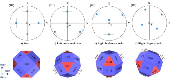
Indeed, a horizontal successive twinning and a horizontal twinning (Fig. 3a), followed by a successive diagonal twin nucleation occur at the left and right side of the sample, respectively. The initial nucleation of those twins is realized at the edge of the sample (Fig. 4, Fig. 5 and Fig.6) where a SLV/C – PL is present. The formed twin boundaries are identified as coherent and symmetrical Σ3 <111> / {111}1,2. As shown in the stereographic projection of the {111} of
the seed (Fig. 8a), there are two {111} having a vertical projection parallel to the growth direction (x) and two {111} presenting a horizontal projection perpendicular to the growth direction (y). In the present case, the first twin nucleus is formed at the edge of the sample on the {111} facet having the horizontal projection (which is confirmed by the a common {111} plane of the seed (Fig. 8a)) and the left horizontal twin (Fig. 8b), at a point where the facet intersects the SLV – PL and is in contact with the crucible wall as well. The free energy of a twinned nucleus is higher than the energy of an untwinned nucleus. However, when the twinned nucleus contains a {111} facet at the triple phase line, its free energy is lower compared to the correctly oriented nucleus, since the free energy of the {111} is lower than that of all other planes in the lattice [39]. Twinning is then possible from an energetical point of view .
In order for nucleation to occur, an increased undercooling at the area close to the edge of the sample is necessary. As proposed by Hurle [42], for a sufficiently large undercooling, the reduction in free energy due to the presence of the low energy plane at the triple point line will exceed the increase in free energy due to the presence of the twin plane. That means that the formation of a twinned nucleus is thermodynamically favored under the presence of a sufficiently large undercooling. In the present work, the measurement of the exact undercooling temperature at the edge of the sample at the instant of the first twin nucleation is not possible due to the fast evolution of the phenomenon and to the needed accuracy of the temperature measurements. However, the growth rate can be quantified by measuring the height of the solid – liquid interface as a function of time and the result is presented in Fig. 9. It becomes clear that
the twin formation is always accompanied by a significant increase in the local growth rate, despite that the externally imposed cooling rate remains constant (-0.2 K/min) all along the experiment.
Moreover, it is confirmed that the growth rate of the global interface is constant (see red curve in Fig. 9), so, it means that a local higher undercooling at the edge of the sample, in comparison to the average undercooling at the solid – liquid interface, exists and has been estimated at about 0.27 K which is sufficient to initiate the observed twin nucleation. As shown in Fig. 4b, at the left edge of the sample, after the initial twin nucleation, the horizontal twin grain grows vertically very fast. Its height is limited by the position of the liquidus melting isotherm (indicated by H in Fig. 4 b), determining in advance the final height of the formed horizontal twin grain. When the first nucleus arrives at the liquidus, stabilization of the growth rate is observed due to the release of the latent heat of solidification until the moment that the solid – liquid interface of the whole sample arrives at the liquidus. This assumption can be confirmed by the growth rate plateau observed in Fig. 9 after each twin nucleation. After nucleation, the twin grows laterally with a rough solid – liquid interface with macro steps, as shown in the X-ray radiography images (Fig. 4b), towards the center of the sample. This growth mechanism is repeated as soon as the undercooling at the edge of the sample is again high enough to form an appropriately oriented new two dimensional twin nucleus. The nucleation always occurs on the common {111} facet that presents a horizontal projection (Fig. 8a and b) followed by a successive alternation of the crystallographic orientation between the one that corresponds to the seed and the other that corresponds to the left horizontal twin Fig. 2. Consequently, this growth model observed in real time can explain the successive twinning growth mechanism experimentally observed.
At the right side of the sample, similarly to the left side, the first twin nucleasion occurs on the {111} facet of the seed that presents a horizontal projection, following the nucleation
mechanism described previously (Fig. 8b and c). The formed grain V has the same crystallographic orientation with the left horizontal twin and grows vertically and laterally on the {111} facet as well, where it becomes in competition with the vertically grown grain in the center of the sample (Fig. 5a). However, despite the fact that twin nucleation is initiated again at the edge of the sample during the solidification process, successive horizontal twinning does not occur. The second twin preferentially nucleates at the edge of the sample on the diagonal {111} facet (Fig. 8c) instead of the horizontal one as illustrated in Fig. 6. The formed twin then grows laterally along the facet. Its vertical growth is very quickly blocked by the formation of a new twin that has the orientation of the first horizontal twin. The nucleation occurs again at the right edge of the sample on the common diagonal {111} facet of the first diagonal (Fig. 8d) and of the first horizontal twin (Fig. 8c). The phenomenon is repeated by the alternation of two crystallographic orientations (the orientation of the first horizontal and first diagonal twin) leading to the formation of the observed successive diagonally inclined twinning (Fig. 2). The second twin preferential nucleation on the diagonal {111} facet instead of the horizontal {111} facet is a consequence of the higher undercooling present at the level of the diagonal facet. This is confirmed by the observation of the X-ray radiography dynamical images of the growing solid – liquid interface (Fig. 6) in this region. From these images, we were able to estimate the undercooling corresponding to the horizontal facet (0.17 K) and to the diagonal one (0.35 K).
4.2 Grain competition and twin nucleation at the solid – solid – liquid triple phase lines (SSL-TPL)
As seen before, the twin crystals that nucleate at the edges of the sample extend towards the central part of the sample and they become in competition with the grains that grow vertically along the growth direction. As growth proceeds, this grain competition results in the groove formation and the nucleation of new twin crystals at the SSL – TPL, leading to the generation of new grain boundaries and thus determining the final solidified Si structure. The
above mentioned mechanisms are examined in this section with a particular focus on the crystallographic orientation of the grains and the energetically favourable grain boundary type formation. Fig. 10a presents a zoom image of the zone α in Fig. 3a. The grain I (Fig. 10a) has the same orientation as the first left horizontal twin and the stereographic projection of its {111} can be seen in Fig. 8b, while grain IV (Fig. 10a) has the same orientation as the initial seed and the stereographic projection of its {111} can be seen in Fig. 8a. During growth, the grain I grows laterally and it becomes in competition with the vertically growing grain III. This competition has for consequence the nucleation of the twin grain II. It should be stressed that this is not an isolated observation but, on the contrary, it happens repeatedly following exactly the development of the horizontal twins. It is well known that the formation of a Σ3 <111> grain boundary is always the most favourable since it has the lowest boundary energy, followed by a Σ9 <110> and then a Σ27a <110> as the most unfavourable of the three types. Based on the orientations of grain I and III, a Σ9 <110> / {114}1,2 that macroscopically deviates by 6° from
the {114} is formed at the encounter of those two grains. The formation of the Σ9 <110> / {114}1,2 grain boundary cannot be seen in Fig. 10a, due to the magnification of the image, but
its presence is visible at a similar triple point at an earlier stage of the solidification (see Fig. 3a) and is observed for all the successive twins sharing the same orientation. The fact though that a vertical and coherent Σ3 <111> grain boundary is replaced by a misoriented Σ9 <110> / {114}1,2 grain boundary created after the encounter of grains I and III seems to influence the
grain boundary energy enough to cause a twinning event. It is believed that this is the driving force for the nucleation of grain II.
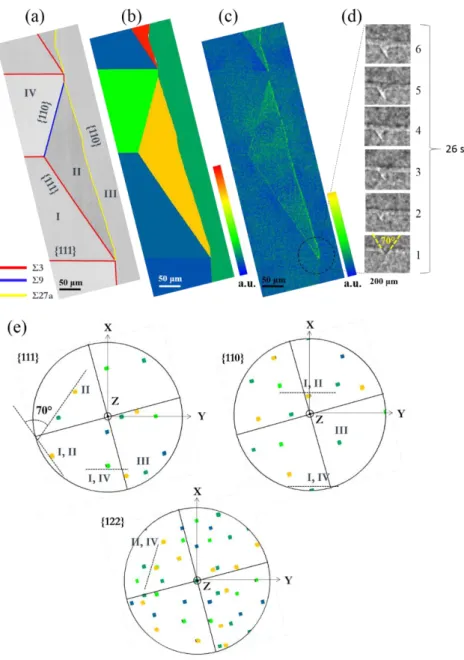
According to the model of Duffar and Nadri [43] and experimentally confirmed by Tandjaoui et al. [27], at the grain – grain – liquid triple phases, that correspond to the intersection of a grain boundary with the solid / liquid interface, grain boundary grooves are formed and can have one of the following three configurations, depending on the
crystallographic orientations of the adjacent grains: i) rough solid – liquid interface on both sides of the groove, ii) rough / facetted groove, iii) facetted / facetted groove. The facets that form the groove have {111} crystallographic orientation. In the present case, after the nucleation of grain II, the grain boundary between grain I and II forms a facetted – facetted groove at the solid – liquid interface, as revealed by the dynamic observation of the solidification process by the X-ray radiography measurements (Fig. 10d_1). The angle between the two facets that form the groove is in accordance with the respective crystallographic orientations of the grains I and II as confirmed by the stereographic projections of their {111} (Fig. 10e). Indeed, it can be seen on this figure that the facetted – facetted groove observed in Fig. 10d_1 is formed due to the encounter of the common {111} of grain I and II (superimposed yellow – blue spot / dotted line) and the {111} of grain II (yellow spot / dotted line). We checked that the 70 ° groove observed in Fig. 10.d_1 corresponds to the angle between the {111} from grains I and II (Fig. 10e). In the general case, when two adjacent grains have no specific crystallographic relation, when a facetted / facetted groove is formed at the solid – liquid interface, the two facets have the same growth rate. As a consequence, the grain boundary between both grains follows the bisector of the angle of the grain boundary groove. This is not the case here for the groove formed at the solid-liquid interface between grains I and II. The reason is that they are in twin Σ3 <111> relation as confirmed by the CSL map (Fig. 10a). For this specific case, the twin grain II nucleates on the common {111} facet between grains I and II (the left hand side facet on Fig. 10d) and propagates along the facet similarly to the lateral growth characterised previously (Fig. 4) and can be seen on Fig. 10d as well.
Due to the grain competition between grains II and III and their respective crystallographic orientations, a symmetric Σ27a <110> / {511}1,2, misoriented by 4° from the
ideal orientation, grain boundary is formed at the beginning of its formation. However, very quickly during growth, the two competing grains adapt to form a symmetric Σ27a <110> /
{552}1,2 and not misoriented grain boundary. The newly formed grain boundary corresponds to
a less dense packed plane in the CSL, but in the present case it seems that its formations is energetically favourable for the system in comparison to the formation of the denser but misoriented Σ27a <110> / {511}1,2. Its orientation relative to the growth direction implies that
grain III will finally gain the competition with grain II.
As growth proceeds, higher in the sample, grain II is found in competition with both grain IV, which is a horizontal twin that grows laterally on the top of grain I, and grain III. When it encounters the {111} facet of grain IV, a facetted – facetted groove is formed and the grain boundary follows the bisector of the groove that corresponds to a symmetrical Σ9 <110> / {122}1,2 minimizing the interfacial energy of the two planes. The competition between grains
II and III is in favor of grain III so that grain II is finally squeezed between grains III and IV and a vertical Σ3 <111> {111}1,2 is formed at their encounter. The vertical Σ3 <111> {111}1,2
grain boundary is formed due to the macroscopic crystallographic orientations of grain III and IV that present a common and vertical {111}. As growth proceeds, the same phenomenon is repeated successively always initiated from the successive twin nucleation at the edge of the sample.
Similarly to the left side, on the right side of the sample, the horizontal twin that initially nucleates at the edge of the sample, grows laterally and comes in competition with the vertically grown grain on the seed. At their encounter, an incoherent Σ3 <111>/ {112}1,2 and asymmetric
Σ3 <111>/ {115}1 | {111}2 grain boundary is formed until the position ζ (Fig. 3a), where the
nucleation of grain VI occurs (Fig. 5a). The formation of an asymmetric and incoherent grain boundary is not a configuration that minimizes the grain boundary energy, however the system has no other choice since grain V grows laterally following its diagonal {111} facet, as revealed by the X-ray radiography image Fig. 5a to+100s, and those two grains have no {111} in common
non-energetically favorable grain boundary formed, the adjacent grains try to adapt to reach a better energetic configuration. This is characterized by the perturbed shape of the grain boundary which is not as straight as the symmetrical Σ3 <111> grain boundaries and which tends to orient along the growth direction. In the following step, grain VI nucleates. Indeed, the grain boundary energy is reduced if twinning occurs (grain VI) leading to the formation of a low energy coherent Σ3 <111> / {111}1,2 and an asymmetric Σ9 <110> / {115}1 | {111}2 grain
boundary. The analysis of the stereographic projections of the {115} and {111} planes that create the asymmetric Σ9 <110> / {115}1 | {111}2 grain boundary shows that the {111} that
belongs to grain VI is very well oriented, however the {115} that belongs to the vertically grown crystal deviates by 4o from the ideal orientation. This is probably the driving force for the new grain nucleation that occurs at position β (Fig. 3a) leading to the dissociation of the asymmetric Σ9 <110> / {115}1 | {111}2 to a low energy coherent Σ3 <111> / {111}1,2 and a slightly
misoriented (~2o) symmetric Σ27a <110> / {115}1,2 grain boundary. On the one hand, the
vertical low energy coherent Σ3 <111> / {111}1,2 propagates during growth along the whole
field of view. On the other hand the formed Σ27a <110> / {115}1,2 CSL is a high energy
configuration and it favors the nucleation of new twins (successive straight line twins) parallel to the growth direction initiated at position β (Fig. 3a). This twinning occurrence finally leads to the formation of coherent and thus low energy Σ3 <111> / {111}1,2 grain boundaries
elongated to the growth direction resulting in the decrease of the total energy of the system. Fig. 11 is a closer view of the position ε in Fig. 3 showing the CSL, GOS, LMP maps and the stereographic projections of {111}. From the stereographic projection of {111}, it can be confirmed that the facetted – facetted groove observed in the X-ray radiography images presented in Fig. 5b correspond to the {111} corresponding to grains V and VI. As previously observed for grains I and II, those two grains are in twin relation so that growth of grain V proceeds along the common {111} facet between grains V and VI until a new nucleation occurs.
As shown in Fig. 5b nucleation occurs between t0 +857 s and t0 + 862 s on both facets leading
to the blocking of grain VI growth and the generation of grain VII (Fig. 11a). Between grain V and VII an incoherent Σ9 <110> grain boundary, composed of Σ9 <110> / {122}1,2 and Σ9
<110> / {411}1,2 segments, is formed. As already discussed previously, this configuration does
not correspond to a low energy state and for energetical reasons grain VIII nucleates and as a consequence, a coherent Σ3 <111> and an incoherent Σ27a <110> grain boundaries are formed. From this point and higher in the sample, grain V continues to occupy the space.
In the central part of the crystal a main grain takes the initial orientation of the seed and grows vertically along the growth direction. Two elongated grains grow on each sides (Fig. 2) while no grain competition occurs between them, as already observed previously [28]. It is believed that this is due to the fact that those grains have the same crystallographic orientation <110> along the growth direction (x) (Fig. 2) and they also have a common {111} parallel to the growth direction. This leads to the formation of two vertical coherent Σ3 <111> / {111}1,2
grain boundaries (Fig. 3a), that correspond to the the lowest energy and are also oriented parallel to the growth direction, and thus the system is in the most energetically favorable state.
From the examined grain boundary configurations, it becomes clear that: i) a higher energy boundary favors nucleation that creates multiple lower energy grain boundary segments, through multiple twin nucleation, reducing the total system energy and ii) the grain boundary configuration is influenced by the CSL, the orientation of the boundary and the growth direction as well. From our in situ study, we can also conclude that only Σ3 twin grain boundaries nucleate and that other grain boundaries are only consequences of subsequent grain competition.
4.3 Deformation, dislocation generation and interaction with grain boundaries
Several origins of dislocations have been evidenced during our experiments: those coming from the seed and others generated during the growth process. The interactions between dislocations, grains and twin boundaries are analysed.
In the X-ray Bragg diffraction images of the first and fifth melting / solidification cycle (Fig. 7a, b) dislocations (dark lines) can be evidenced because of the strain fields they create that appear as black lines on the diffraction images. Dislocations, originating in the seed and/or generated at the seed / up-grown crystal interface, propagate on a vertical {111} slip plane into the up – grown crystal along the <110> growth direction. The seed crystal is taken from a Czochralski (Cz) ingot and should be dislocation free [44]. However, as shown in the Bragg diffraction images the up – grown dislocations already exist in the initial seed. Depending of the pulling speed or the cooling rate, many point defects cannot be avoided in Cz – Si, such as self-interstitial atoms, vacancies, Frenkel pairs or impurity atoms. The main impurity in Cz material is oxygen which accumulates in interstitial position in the ingot (solid phase) due to its segregation coefficient higher than the unit (1.25), regardless carbon and doping species which are incorporated in substitutional position in the matrix. When oxygen silicide precipitation takes place, or when doping impurities like boron and nitrogen diffuse from the BN crucible via the so – called Goesele mechanism (kick-out) in the silicon seed, self-interstitial atoms can be generated and if they cannot find any sink to be annihilated (like surfaces, voids, dislocations), they agglomerate in disks and form prismatic Frank loops (sessile edge dislocations) or dissociated dislocation loops (loop punching from an oxygen silicide precipitate, for instance). These dislocations can glide in {111} and can propagate throughout the crystal when a thermal or mechanical driving force is present as in our experiments for which the seed is maintained at high temperature close to melting temperature.
Another possible source of the observed dislocations can be the interface between the un-melted seed and the solidified silicon. As presented in the integrated intensity map (Fig. 3b), a slightly distorted zone is formed in the vicinity of this area implying that the up grown crystal does not perfectly adopt the initial orientation of the seed. This is confirmed by the rocking curve measurements where a misorientation of 5 ×10⁻² degrees is found between the seed and the up – grown crystal. M. G. Tsoutsouva et al. [11] have shown that relative misorientations of this order of magnitude can act as sources for the production of dislocations in solidified silicon.
In the case of the first melting / solidification cycle (Fig. 7a), where twinning occurs, the propagation of the vertically grown dislocations is efficiently blocked by the horizontal grain boundary formed with grain B, since they are no longer visible in its interior part. After a crystallographic analysis, it is found that the twin crystal B is in a Σ3 <111> relation with the seed after a rotation of 60° around the (11�1) plane and its diffracting plane corresponds to the (1�11). The twin crystal (B in Fig. 7a) is of high crystallographic quality and no distorted areas are observed in their volume. This implies that the growth dislocations after the intersection with the Σ3 <111> / {111} boundary manage to cross-slip on the two inclined {111} that present a horizontal projection. Due to the small thickness of the sample (0.3 mm) they very quickly reach either the front or the back surface of the sample [45]. Since pure screw dislocations have no preferential glide plane and since a substantial reduction of dislocation density is observed whenever twinning occurs, it is assumed that the generated dislocations in the studied Cz sample during melting/solidification cycles have an edge component.
The same dislocation blocking mechanism is also visible in the integrated intensity map (Fig. 3b) that corresponds to the 13th melting / solidification cycle of the same sample, where the horizontal twin crystal, above the formation of the coherent Σ3 <111> / {111} twin boundary, appears less distorted in comparison to the grown crystal from the initial seed.
From the grain orientation spread map (GOS) in Fig. 10b, that gives an indication of the level of each grain distortion, it can be seen that grain II is the most deformed as compared to the horizontal twins I and IV and grain III. It is strongly believed that this is due to the fact that grain II is in direct competition with those grains so that its development is blocked due to the growth of grains III and IV and at the end it is found to be squeezed at the encounter of the Σ3 <111>, Σ9 <110> and Σ27a <110> grain boundaries. The same phenomenon is also observed in the case of grain VI (Fig. 11b), whose growth is prevented by the nucleation of grain VII on its {111} facet. From the same figure, we can confirm that the multiple twin nucleation of grains VII and VIII that occurs at position ε (Fig. 3a) relaxes the stresses in the growing structure. Lastly, grain VII is less deformed than grain V and VI, and then grain VIII is the least distorted. The grain deformation is directly related to the dislocation density in the inner part of each grain and this is better revealed by the average local misorientation maps (LMP) in Fig. 10c and 11c. In both figures, the grains that appear more distorted in the GOS map (grains II and VI) present also a higher dislocation density in the LMP maps. The LMP (Fig. 10c and 11c) and the rocking curve integrated intensity map (Fig.3b positions α, β and γ) shows that there is a direct relation between the level of distortion and the twin boundary CSL type. On the one hand, all the low coincidence incoherent Σ27a <110> twin grain boundaries are more distorted in comparison to the incoherent Σ9 <110> and to the coherent Σ3 <111>. On the other hand, dislocation generation generally occurs at the encounter of two grain boundaries that belong to different CSL type one of them being a Σ27a <110>. For instance, at the encounter of the Σ27a <110> with the Σ9 <110> and with the Σ3 <111> grain boundaries at position β in Fig. 3a, b and at position γ in Fig. 3a, b respectively , dislocations are emitted from the sharp edge of the grain boundary in the surrounding crystal. This is also visible in the Bragg diffraction images of the first melting/solidification cycle where dislocations are generated at the edges of the grain boundaries between grains A and C with B (Fig. 7). Actually, when a low coincidence and
incoherent twin boundary, such as a Σ27 <110>, which common plane is no longer a glide plane, meet with another grain boundary, dislocations cannot any more easily cross the crystallographic barrier and hence pile up nearby the grain boundary. This causes a drastic increase in the neighboring plane deformation which in turn can transform the grain boundary edge into a stress concentrator and make it behave as dislocation source. On top of that, the character of the grain boundary (coherent - incoherent) and its Σ – type, its deviation from the optimum orientation and the symmetry or non-symmetry of the boundary planes seems to have an impact on the distortion of the formed boundary and on the emission of dislocations in the vicinity of the surrounding grains as well. A representative case is position ζ in Fig. 3a, where, as extensively discussed in details in paragraph 4.2, the incoherent and asymmetric Σ3 <111> grain boundary that deviates from the ideal orientation drives the nucleation of grain VI creating a lower energy coherent Σ3 <111> / {111}1,2 and an asymmetric Σ9 <110> / {115}1 | {111}2
grain boundaries. The {115} plane of the Σ9 <110> / {115}1 | {111}2 grain boundary deviates
from the ideal orientation as well. At this area, as it can be seen in the Bragg diffraction images (Fig. 5a), the zone near those grain boundaries appears darker indicating higher distortion levels in comparison to the central part of the grain. Additionally, higher up, a bunch of dislocations expands in grain VI. It is believed though, that a deviation from the relative orientation of the two adjacent crystals that leads to the formation of grain boundaries that deviate from the ideal coincidence orientation can produce a network of so called secondary dislocations which allow the system to conserve the minimum energy pattern over most of the boundary surface. The existence of such networks was shown among others by Balluffi et al.[46,47] and Bollmann et
al.[48].
Another information that can be extracted from the LMP map (Fig. 11c) is that most of grain V distortion is located at the edge of the grain which is squeezed between grains VI and VII. In this area, it is believed that the accumulation of dislocations introduces local strain that
acts as driving force for the twin VII nucleation parallel to the {111} facet of grain VI. Evidence of this assumption can also be seen in the case of the first melting/solidification cycle (Fig. 7a). The horizontal twin nucleation (grain B) initiated in the central part of the sample is probably favored by the local stresses due to the presence of the vertically grown dislocations. Those results are just an indication that the induced local – stresses can help triggering twin nucleation however, more experimental observations are needed to confirm this hypothesis to further understand the twin nucleation mechanism.
Conclusions
In-situ experiments in combination with X-ray imaging techniques is a powerful tool for
deepening the understanding on the processes involved during solidification. Phenomena that occur during crystal growth such as grain nucleation, grain competition, twin formation, defect generation, their evolution and interaction with grains have be followed and investigated in situ. Once grains have nucleated, they grow and some of them extend, while some others cannot keep growing in the upper part of the sample. Τhe selection mechanism depends on the process parameters (velocity of the solid – liquid interface, temperature gradient, cooling rate) defining the isotherm profiles and evolution and is also directly linked to the relative crystallographic orientation between competing grains. It also depends on the local interface morphology (rough or faceted).
Nucleation of twin crystals is found to occur on {111} facets at the edge of the sample where solid – liquid – vapor triple point lines exist and at the location where the sample is in contact with the crucible as well. Nucleation also takes place at the solid – solid – liquid triple point lines, where two grain are in competition, on the {111} facets of the groove. Twin nucleation is accompanied by a significant increase of the local growth rate related to a higher undercooling than on the global solid – liquid interface. The enhanced undercooling temperature and the stress accumulation are found to be driving forces for the twin grain
nucleation. Moreover, it is observed that coherent Σ3 <111> grain boundaries efficiently blocked the propagation of growth dislocation.
Areas in which Σ27a <110> grain boundaries are present are two times more distorted in comparison to the average distortion of the sample. Dislocations are emitted at the encounter of a Σ27a <111> grain boundary with either a Σ3 <111> or a Σ9 <110> grain boundary. On top of that, the character of the grain boundary (coherent – incoherent), its Σ – type, its deviation from the optimum orientation and the symmetry or non-symmetry of the boundary planes have an impact on the distortion of the formed boundary and on the emission of dislocations in the vicinity of the surrounding grains as well.
From those experiments, it becomes obvious that twinning observed in our ingots is a growth rather than a deformation phenomenon. Moreover and importantly, only Σ3 twins nucleate during growth, higher order grain boundaries being the result of grain competition. The samples containing low dislocation density present large number of areas containing multiple twins and vice versa. In general, the nucleation of twins is thermodynamically unfavorable since it increases the total system energy by adding new grain boundaries. However, from this work it is brought in evidence that twinning that results in the grain boundary dissociation have always the tendency to relax the stresses developed in the crystal during the growth process. Grains that are in direct competition with other grains and / or squeezed in – between grain boundaries are more deformed and contain higher density of dislocations but during growth their development is prevented and their size remains limited.
Acknowledgment
This work is funded by the ANR Project CrySaLID (N° ANR-14-CE05-0046-01). The ESRF (European Synchrotron Radiation Facility) BM05 team is greatly acknowledged for support during the X-ray imaging experiments and J. Hardwick for the X-ray diffraction rocking curve imaging measurements.
References
[1] K. Fujiwara, W. Pan, N. Usami, K. Sawada, M. Tokairin, Y. Nose, A. Nomura, T. Shishido, K. Nakajima, Growth of structure-controlled polycrystalline silicon ingots for solar cells by casting, Acta Mater. 54 (2006) 3191–3197.
[2] T.F. Li, H.C. Huang, H.W. Tsai, A. Lan, C. Chuck, C.W. Lan, An enhanced cooling design in directional solidification for high quality multi-crystalline solar silicon, J. Cryst. Growth. 340 (2012) 202–208.
[3] K. Nakajima, K. Kutsukake, K. Fujiwara, K. Morishita, S. Ono, Arrangement of dendrite crystals grown along the bottom of Si ingots using the dendritic casting method by controlling thermal conductivity under crucibles, J. Cryst. Growth. 319 (2011) 13–18. [4] A. Jouini, D. Ponthenier, H. Lignier, N. Enjalbert, B. Marie, B. Drevet, E. Pihan, C.
Cayron, T. Lafford, D. Camel, Improved multicrystalline silicon ingot crystal quality through seed growth for high efficiency solar cells, Prog. Photovolt. Res. Appl. 20 (2012) 735–746.
[5] M. Trempa, C. Reimann, J. Friedrich, G. Müller, D. Oriwol, Mono-crystalline growth in directional solidification of silicon with different orientation and splitting of seed crystals, J. Cryst. Growth. 351 (2012) 131–140.
[6] K.E. Ekstrøm, G. Stokkan, R. Søndenå, H. Dalaker, T. Lehmann, L. Arnberg, M. Di Sabatino, Structure and dislocation development in mono-like silicon, Phys. Status Solidi A. 212 (2015) 2278–2288.
[7] V.A. Oliveira, M. Rocha, T.N. Tran Thi, M. Tsoutsouva, J. Baruchel, D. Camel, Cellular dislocation patterns in “Mono-like” silicon grown by seeded directional solidification of the melt, in: ECCG5 Proc., Bologna, Italy, 2015.
[8] V.A. Oliveira, M. Tsoutsouva, T. Lafford, E. Pihan, F. Barou, D. Camel, Sub-grain boundaries sources and effects in large mono-like silicon ingots for PV, in: EU PVSEC Proc., Amsterdam, Netherlands, 2014: pp. 793–797.
[9] M. Trempa, C. Reimann, J. Friedrich, G. Müller, A. Krause, L. Sylla, T. Richter, Influence of grain boundaries intentionally induced between seed plates on the defect generation in quasi-mono-crystalline silicon ingots, Cryst. Res. Technol. 50 (2015) 124– 132.
[10] M. Trempa, C. Reimann, J. Friedrich, G. Müller, A. Krause, L. Sylla, T. Richter, Defect formation induced by seed-joints during directional solidification of quasi-mono-crystalline silicon ingots, J. Cryst. Growth. 405 (2014) 131–141.
[11] M.G. Tsoutsouva, V.A. Oliveira, D. Camel, J. Baruchel, B. Marie, T.A. Lafford, Mono-like silicon ingots grown on low angle misoriented seeds: Defect characterization by synchrotron X-ray diffraction imaging, Acta Mater. 88 (2015) 112–120.
[12] M.G. Tsoutsouva, V.A. Oliveira, D. Camel, T.N. Tran Thi, J. Baruchel, B. Marie, T.A. Lafford, Segregation, precipitation and dislocation generation between seeds in directionally solidified mono-like silicon for photovoltaic applications, J. Cryst. Growth. 401 (2014) 397–403.
[13] F. Jay, D. Muñoz, T. Desrues, E. Pihan, V. Amaral de Oliveira, N. Enjalbert, A. Jouini, Advanced process for n-type mono-like silicon a-Si:H/c-Si heterojunction solar cells with 21.5% efficiency, Sol. Energy Mater. Sol. Cells. 130 (2014) 690–695.
[14] K. Jiptner, M. Fukuzawa, Y. Miyamura, H. Harada, T. Sekiguchi, Effect of Crystallinity on Residual Strain Distribution in Cast-Grown Si, Jpn. J. Appl. Phys. 52 (2013) 65501. [15] D. Zhu, L. Ming, M. Huang, Z. Zhang, X. Huang, Seed-assisted growth of high-quality
[16] Y.T. Wong, C. Hsu, C.W. Lan, Development of grain structures of multi-crystalline silicon from randomly orientated seeds in directional solidification, J. Cryst. Growth. 387 (2014) 10–15.
[17] R.R. Prakash, T. Sekiguchi, K. Jiptner, Y. Miyamura, J. Chen, H. Harada, K. Kakimoto, Grain growth of cast-multicrystalline silicon grown from small randomly oriented seed crystal, J. Cryst. Growth. 401 (2014) 717–719.
[18] C. Reimann, M. Trempa, T. Lehmann, K. Rosshirt, J. Stenzenberger, J. Friedrich, K. Hesse, E. Dornberger, Influence of different seed materials on multi-crystalline silicon ingot properties, J. Cryst. Growth. 434 (2016) 88–95.
[19] K. Kutsukake, M. Deura, Y. Ohno, I. Yonenaga, Characterization of silicon ingots: Mono-like versus high-performance multicrystalline, Jpn. J. Appl. Phys. 54 (2015) 08KD10. [20] E.-R. Carl, A. Danilewsky, E. Meissner, T. Geiger, Large- and small-angle grain
boundaries in multi-crystalline silicon and implications for the evolution of grain boundaries during crystal growth, J. Appl. Crystallogr. 47 (2014) 1958–1965.
[21] G. Stokkan, Twinning in multicrystalline silicon for solar cells, J. Cryst. Growth. 384 (2013) 107–113.
[22] Ervik, T., Kivambe, M., Stokkan, G., Ryningen, B., Lohne, O., Dislocation formation at ∑27a boundaries in multicrystalline silicon for solar cells, in: EU PVSEC Proc., Hamburg, Germany, 2011: pp. 1895–1899.
[23] T. Duffar, C.T. Nwosu, I.M. Asuo, J. Muzy, N.D.Q. Chau, Y. Du Terrail-Couvat, F. Robaut, Experimental study of grain boundary orientations in multi-crystalline silicon, J. Cryst. Growth. 401 (2014) 404–408.
[24] P. Käshammer, T. Sinno, Interactions of twin boundaries with intrinsic point defects and carbon in silicon, J. Appl. Phys. 114 (2013) 83505.
[25] A. Autruffe, V. Stenhjem Hagen, L. Arnberg, M. Di Sabatino, Dislocation generation at near-coincidence site lattice grain boundaries during silicon directional solidification, J. Cryst. Growth. 411 (2015) 12–18.
[26] A. Tandjaoui, N. Mangelinck-Noël, G. Reinhart, J.-J. Furter, B. Billia, T. Lafford, J. Baruchel, X. Guichard, Real Time Observation of the Directional Solidification of Multicrystalline Silicon: X-ray Imaging Characterization, Energy Procedia 27 (2012) 82– 87.
[27] A. Tandjaoui, N. Mangelinck-Noel, G. Reinhart, B. Billia, T. Lafford, J. Baruchel, Investigation of grain boundary grooves at the solid–liquid interface during directional solidification of multi-crystalline silicon: in situ characterization by X-ray imaging, J. Cryst. Growth. 377 (2013) 203–211.
[28] T. Riberi-Béridot, N. Mangelinck-Noël, A. Tandjaoui, G. Reinhart, B. Billia, T. Lafford, J. Baruchel, L. Barrallier, On the impact of twinning on the formation of the grain structure of multi-crystalline silicon for photovoltaic applications during directional solidification, J. Cryst. Growth. 418 (2015) 38–44.
[29] A. Tandjaoui, N. Mangelinck-Noel, G. Reinhart, B. Billia, X. Guichard, Twinning occurrence and grain competition in multi-crystalline silicon during solidification, C R Phys. 14 (2013) 141–148.
[30] J.-C. Labiche, O. Mathon, S. Pascarelli, M.A. Newton, G.G. Ferre, C. Curfs, G. Vaughan, A. Homs, D.F. Carreiras, Invited article: The fast readout low noise camera as a versatile x-ray detector for time resolved dispersive extended x-ray absorption fine structure and diffraction studies of dynamic problems in materials science, chemistry, and catalysis, Rev. Sci. Instrum. 78 (2007) 91301.
[31] D. Lübbert, T. Baumbach, J. Härtwig, E. Boller, E. Pernot, μm-resolved high resolution X-ray diffraction imaging for semiconductor quality control, Nucl. Instrum. Methods Phys. Res. Sect. B Beam Interact. Mater. At. 160 (2000) 521–527.
[32] J. Hoszowska, A.K. Freund, E. Boller, J.P.F. Sellschop, G. Level, J. Härtwig, R.C. Burns, M. Rebak, J. Baruchel, Characterization of synthetic diamond crystals by spatially resolved rocking curve measurements, J. Phys. Appl. Phys. 34 (2001) A47.
[33] P. Mikulík, D. Lübbert, P. Pernot, L. Helfen, T. Baumbach, Crystallite misorientation analysis in semiconductor wafers and ELO samples by rocking curve imaging, Appl. Surf. Sci. 253 (2006) 188–193.
[34] M. Calamiotou, N. Chrysanthakopoulos, G. Papaioannou, J. Baruchel, Dynamics of photodeformations and space charge field in photorefractive Fe:LiNbO3 studied with synchrotron area diffractometry, J. Appl. Phys. 102 (2007) 83527.
[35] M.G. Tsoutsouva, V.A. Oliveira, J. Baruchel, D. Camel, B. Marie, T.A. Lafford, Characterization of defects in mono-like silicon for photovoltaic applications using X-ray Bragg diffraction imaging, J. Appl. Crystallogr. 48 (2015) 645–654.
[36] T.N. Tran Thi, S. Dubois, J. Baruchel, N. Enjalbert, B. Fernandez, T. Schülli, T.A. Lafford, Czochralski and mono-like p-type and n-type silicon solar cells: Relationship between strain and stress induced by the back contact, and photovoltaic performance, Sol. Energ. Mat. Sol. Cells. 135 (2015) 17–21.
[37] S.I. Wright, M.M. Nowell, D.P. Field, A Review of Strain Analysis Using Electron Backscatter Diffraction, Microsc. Microanal. 17 (2011) 316–329.
[38] V.V. Voronkov, Processes at the boundary of a crystallization front, Son. Phys. Crystallogr. 19 (1975) 573–577.