HAL Id: hal-00409024
https://hal.archives-ouvertes.fr/hal-00409024
Submitted on 5 Aug 2009
HAL is a multi-disciplinary open access
archive for the deposit and dissemination of
sci-entific research documents, whether they are
pub-lished or not. The documents may come from
teaching and research institutions in France or
abroad, or from public or private research centers.
L’archive ouverte pluridisciplinaire HAL, est
destinée au dépôt et à la diffusion de documents
scientifiques de niveau recherche, publiés ou non,
émanant des établissements d’enseignement et de
recherche français ou étrangers, des laboratoires
publics ou privés.
Shall we trust WDDL?
Sylvain Guilley, Sumanta Chaudhuri, Laurent Sauvage, Tarik Graba,
Jean-Luc Danger, Philippe Hoogvorst, Vinh-Nga Vong, Maxime Nassar,
Florent Flament
To cite this version:
Sylvain Guilley, Sumanta Chaudhuri, Laurent Sauvage, Tarik Graba, Jean-Luc Danger, et al.. Shall we
trust WDDL?. Future of Trust in Computing, Jun 2008, Berlin, Germany. pp.208-215,
�10.1007/978-3-8348-9324-6_22�. �hal-00409024�
Shall we trust WDDL?
Sylvain GUILLEY
Sumanta CHAUDHURI
Laurent SAUVAGE
Tarik GRABA
Jean-Luc DANGER
Philippe HOOGVORST
Vinh-Nga VONG
Maxime NASSAR
Florent FLAMENT
Institut TELECOM, TELECOM ParisTech
CNRS LTCI (UMR 5141)
D´epartement COMELEC, 46 rue Barrault
75 634 PARIS Cedex 13, FRANCE
<
firstname.lastname@TELECOM-ParisTech.fr
>
Abstract
Security is not only a matter of cryptographic algorithms robustness but becomes also a question of securing their implementation. P. Kocher’s Differential Power Analysis (DPA) is one of the many side-channel attacks that are more and more studied by the security commu-nity. Indeed, side-channel attacks (SCA) have proved to be very powerful on cryptographic algorithms such as DES and AES, customarily implemented in a wide variety of devices, ranging from smart-cards or ASICs to FPGAs. Among the proposed countermeasures, the “dual-rail with precharge logic” (DPL) aims at hiding information leaked by the circuit by making the power consumption independent of the calculation. However DPL logic could be subject to second order attacks exploiting timing difference between dual nets. In this article, we characterize by simulation, the vulnerability due to timing unbalance in the eight DES substitution boxes implemented in DPL WDDL style. The characterization results in a clas-sification of the nodes according to their timing unbalance. Our results show that the timing unbalance is a major weakness of the WDDL logic, and that it could be used to retrieve the key using a DPA attack. This vulnerability has been experimentally observed on a full DES implementation using WDDL style for Altera Stratix EP1S25 FPGA.
Keywords: differential power analysis (DPA), side-channel attacks (SCA), secure logic style, dual-rail with precharge logic (DPL), wave dynamic differential logic (WDDL), early evaluation, timing unbalance.
1
Introduction
The principle of “dual-rail with precharge logic” (DPL) is to protect the implementation against side-channel attacks such as the Differential Power Analysis (DPA) [4]. The DPL is a two-phase protocol composed of a precharge phase and a evaluation phase. Each signal is represented in dual-rail logic by its “true” and “false” parts, which are complementary. During the precharge phase, all signals are put in an initial state (assumed to be 00 in the sequel) to ensure that during the evaluation phase, the number of computations is fully predictable and constant whatever the inputs. In this article, we focus on the the “Wave Dynamic Differential Logic” (WDDL), a DPL based on standard cell flow, proposed by K. Tiri [6].
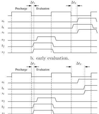
However as described by D. Suzuki [5], DPL logic can still leak information because “true” and “false” parts can evaluate at different time according to the inputs. The root of this problem is the early evaluation. As a matter of fact, such difference in delay time will appear when early evaluation is combined with other unbalance factors, such as: difference of logical paths or unbalance of dual
nets. Fig.1b illustrates the principle of early evaluation for a 2-input AND gate and its dual 2-input ORgate, as represented on the Fig. 1a.
‘True’ half OR ‘False’ half AND st sf at bt af bf a. WDDL circuit example. Precharge Evaluation bt bf sf af at ∆t1 ∆t2 st b. early evaluation. Precharge Evaluation bf sf ∆t1 ∆t2 st bt at af
c. early evaluation combined with unbalance of dual net.
Figure 1: Illustrations of dual-rail timing unbalance.
We observe that, depending on the inputs value, the switching delay time differs because of the early evaluation in AND and OR gates. In this example, it is clear that the OR gate evaluates as soon as one of its inputs is set to ’1’, on an other hand, the AND gate must wait until each of its entries are set to ’1’, in order to switch its output. Of course, the opposite behavior would take place if the first available input would have been set to ’0’ (the AND gate would have evaluated immediately and the OR gate would have waited for every inputs to be set).
Early evaluation is then linked to the equations defining the circuit and exhibits the timing difference between signal a and b. In addition, for dual-rail logic, the difference of delay time could also be strengthened by two main factors:
1. The unbalance between the “true” and “false” nets, due to placement and routing differences, produces a timing difference between the true and the false net of a dual rail signal. In fact, if btis slower than bf, the delay time ∆t2 could increase as shown on Fig.1c.
2. The unbalance of logical paths between inputs of a given logical gate, due to the fact that some inputs have to pass through more logical layers than others, leads to a timing difference between these input signals on each half path. In the same way, if a is slower than b, ∆t2
could also increase significantly.
To summarize, the switching time of output s (st,sf) depends on the inputs a (at,af) and b
(bt,bf). As well as the switching time difference between st and sf depends on the inputs. As a
consequence, if for one signal, ∆t defined as ∆t= ∆t. 1−∆t2, can be detected by an instrument, the
activity of the node could be monitored and this can lead to the secret key. In order to estimate if this vulnerability could be exploited on a real design, we have simulated the eight DES substitution boxes (S-Boxes) implemented in WDDL on an Altera Stratix FPGA and analyzed the switching timing delay for every node of the S-boxes.
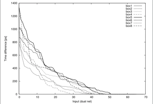
0 200 400 600 800 1000 1200 1400 0 10 20 30 40 50 60 70 Time difference [ps]
Input (dual net)
box1 box2 box3 box4 box5 box6 box7 box8
Figure 2: ∆t decrease for the eight DES 6 7→ 4 S-Boxes.
So far, difference in timing delay has only been studied on elementary designs, consisting of a single gate. Our objective is to assess whether or not this observation scales up to a full-fledged hardware encryption accelerator (in our case triple-DES on FPGA). To reach our goal, we first evaluate the vulnerability by simulation, and then effectively attack the physical implementation. The remainder of the paper is structured as follows: Sec.2 presents the methods used to analyze the timing unbalance in dual-rail logic, Sec.3presents how WDDL could be successfully attacked based on a criterion defined in Sec.2. Finally, the section4concludes this article. The appendixA
provides with some precisions about the simulations realized in Sec.2.
2
Timing Analysis of Differential Logic
We simulate the post-placed and routed compact substitution boxes (S-Boxes) designed specifically for FPGA as described in [1]. Each DES S-Box has a 6-bit input and a 4-bit output. The simulation environment provides the precharge and evaluation phases for all possible inputs. The main information extracted from the Value Change Dump (VCD) output file is the switching delay of each net during the precharge and evaluation phases. The switching delay is defined as the delay for one net to switch after the inputs are set. In our evaluations, we calculate for each node the absolute difference between the mean switching delay of the true net, and the mean switching delay of the false net. We call this difference ∆t. The nodes of the S-Box are then ordered in descending ∆t. The results are plotted for the eight S-boxes in Figure.2.
According to Figure.2, the most vulnerable S-Box seems to be box5 for two main reasons: ∆t is the highest and its decrease is the slowest.
The analysis yields a classification of the nodes according to their vulnerability, namely the ∆t. In order to exploit this information for real attack, the following methodology is applied:
1. First selection: find nodes where ∆t is higher than 1 ns (for experimental reasons: the timing difference should be visible with a sampling rate of 20 Gs/s and a bandwidth of 5 GHz).
2. Second selection: Among the nodes in the first selection, find the nodes where the dispersion of the switching delay do not overlap.
3. Third selection: Among the nodes in the second selection, select the ones having the smallest dispersion.
Figure. 3 presents the node selected for the eight S-Boxes of DES. It displays the repartition in time of the switching delay for the “true” and “false” nets. The node in box5 with nets wire e trueand wire 1 f alse is chosen as the most vulnerable and will be used for a DPA attack on the DES implementation on our Altera Stratix FPGA (model EP1S25, in 130 nm technology). The separation between “true” and “false” evaluation dates is especially eloquent for S-Boxes 3, 4, 5 & 8.
Moreover, the simulation on the 26
= 64 possible inputs for the S-Boxes is also an easy way to extract information on the activity of each node. In fact, to apply a DPA on power traces collected on a real implementation, one should be able to define the selection function which depends on the node under attack. Based on the simulation, we can extract for each net, the list of inputs that make it switch, and therefore the selection function for the DPA.
3
Practical Test on DES WDDL Implemented in an Altera
Stratix EP1S25 FPGA
In order to validate the results obtained by simulation, we have performed a DPA attack on the node identified as the more vulnerable. We mention that attacks based on correlations with one single bit do work in practice on unprotected implementations. A differential trace after a single-bit correlation can be seen in Fig. 2 of [3] or in Fig. 4.
As our objective here is only to validate that the timing difference for dual nets is visible, we make the correct assumption for the key and perform the DPA with the correct selection function. Figure. 5 shows the result of the DPA. We observe that the results match the expectation, e.g. that the DPA shows a spike that betrays the incriminated correlation.
4
Conclusion
Dual-rail with Precharge Logic (DPL) is a technique that ensures that upon execution, a circuit always toggles the same number of nodes during each clock cycle. This technique reduces signif-icantly the information leakage on the power side channel (see left part of Figure.5). With this technology, the attack based on the correlation between the key and the number of nodes toggled at a given clock cycle, is not possible anymore.
However some DPL technologies, such as WDDL, still leak information over the power side channel (see right part of Figure.5). The switching timing difference between dual nets of some internal nodes is correlated to the data being computed. The power consumption profile of such chip is therefore exploitable to lead a side-channel attack.
We conclude that this correlation can be exploited for some nodes where the timing difference is significant enough. In addition, the analysis of the simulation leads to a classification of the nodes according to their vulnerability. For the first time, it has been proved that such correlation could be exploited on experimental traces. Finally, this article leads to the conclusion that the timing unbalance of dual nets should allow power consumption attacks.
References
[1] Sylvain Guilley, Sumanta Chaudhuri, Laurent Sauvage, Tarik Graba, Jean-Luc Danger, Philippe Hoogvorst, Vinh-Nga Vong, and Maxime Nassar. Place-and-Route Impact on the Security of DPL Designs in FPGAs. In HOST, IEEE, pages 29–35, jun 2008. June 9, Anaheim, USA. ISBN = 978-1-4244-2401-6.
[2] Sylvain Guilley, Laurent Sauvage, Jean-Luc Danger, Nidhal Selmane, and Renaud Pacalet. Silicon-level solutions to counteract passive and active attacks. In FDTC, 5th Workshop on Fault Detection and Tolerance in Cryptography, IEEE-CS, pages 3–17, Washington DC, USA, aug 2008. (Up-to-date version on HAL:
http://hal.archives-ouvertes.fr/hal-00311431/en/).
[3] Thanh-Ha Le, C´ecile Canovas, and Jessy Cl´edi`ere. An overview of side channel analysis at-tacks. In ASIACCS, pages 33–43. ASIAN ACM Symposium on Information, Computer and Communications Security, 2008. DOI: 10.1145/1368310.1368319. Tokyo, Japan.
[4] P. Kocher and J. Jaffe and B. Jun. Differential Power Analysis. In Proceedings of CRYPTO’99, volume 1666 of LNCS, pages 388–397. Springer-Verlag, 1999. (PDF).
[5] Daisuke Suzuki and Minoru Saeki. Security Evaluation of DPA Countermeasures Using Dual-Rail Pre-charge Logic Style. In CHES, volume 4249 of LNCS, pages 255–269. Springer, 2006.
http://dx.doi.org/10.1007/11894063_21.
[6] Kris Tiri and Ingrid Verbauwhede. A Logic Level Design Methodology for a Secure DPA Resistant ASIC or FPGA Implementation. In DATE’04, pages 246–251. IEEE Computer Society, February 2004. Paris, France.
S-Box 1 S-Box 2 0 20 40 60 80 100 0 2 4 6 8 10 Bin count [%] Delay [ns] wire_9a7a_false wire_6585_true 0 20 40 60 80 100 0 2 4 6 8 10 Bin count [%] Delay [ns] wire_c3e45a1b_true wire_3c1ba5e4_false S-Box 3 S-Box 4 0 20 40 60 80 100 0 2 4 6 8 10 Bin count [%] Delay [ns] wire_c3b6_true wire_3c49_false 0 20 40 60 80 100 0 2 4 6 8 10 Bin count [%] Delay [ns] wire_4bb8_false wire_b447_true S-Box 5 S-Box 6 0 20 40 60 80 100 0 2 4 6 8 10 Bin count [%] Delay [ns] wire_e_true wire_1_false 0 20 40 60 80 100 0 2 4 6 8 10 Bin count [%] Delay [ns] wire_969b_true wire_6964_false S-Box 7 S-Box 8 0 20 40 60 80 100 0 2 4 6 8 10 Bin count [%] Delay [ns] wire_d835_true wire_27ca_false 0 20 40 60 80 100 0 2 4 6 8 10 Bin count [%] Delay [ns] wire_b1_true wire_4e_false
-0.2 -0.1 0 0.1 0.2 0.3 0.4 2 1 0 -1
Voltage drop across a 10
Ω resistor [mV] DES round (R0 ⊕ R1)[1] -0.2 -0.1 0 0.1 0.2 0.3 0.4 2 1 0 -1
Voltage drop across a 10
Ω resistor [mV] DES round (R0 ⊕ R1)[2] -0.2 -0.1 0 0.1 0.2 0.3 0.4 2 1 0 -1
Voltage drop across a 10
Ω resistor [mV] DES round (R0 ⊕ R1)[3] -0.2 -0.1 0 0.1 0.2 0.3 0.4 2 1 0 -1
Voltage drop across a 10
Ω
resistor [mV]
DES round
(R0 ⊕ R1)[4]
Figure 4: Example of four mono-bit differential trace on SecMatV1 DES [2, §2.1].
-0.0002 -0.00015 -0.0001 -5e-05 0 5e-05 1e-04 0.00015 0.0002 0 5000 10000 15000 20000
Side-channel leakage (EMA)
Samples [ 20Gsample/s]
Naturally balanced net
-0.0002 -0.00015 -0.0001 -5e-05 0 5e-05 1e-04 0.00015 0.0002 0 5000 10000 15000 20000
Side-channel leakage (EMA)
Samples [ 20Gsample/s]
Naturally unbalanced net
Figure 5: Experimental covariance between the power traces and a regular net (left – no leakage) & the most critical net value (right – very leaky, see peak around sample 5,000).
A
Appendix: Details on Simulation and Timing Analysis
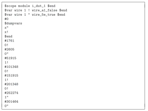
Table 1: Example of VCD file for a given gate.
$scope module i_dut_1 $end $var wire 1 ! wire_a1_false $end $var wire 1 " wire_5e_true $end #0 $dumpvars x" x! $end #1761 0! #2605 0" #51915 1! #101348 0! #151915 1! #201348 0! #252274 1" #301464 0"
The code snippet of Tab. 1 gives an example the VCD syntax. Tab.2 presents an extract of the nodes classification for S-Box 5.
Table 2: Extract of nodes classification for S-Box 5.
delta_t wire/port name activity mean delay(ps) std dev 1336 wire_9a95_false 32 5224.00 738.12 wire_656a_true 32 3888.00 318.50 1152 wire_e_true 48 1696.00 116.12 wire_1_false 16 2848.00 7.00 1104 wire_9569_true 32 5096.00 469.32 wire_6a96_false 32 3992.00 250.02 1024 wire_3a5c_false 32 4416.00 269.61 wire_c5a3_true 32 3392.00 222.74 976 wire_69_false 32 4656.00 199.41 wire_96_true 32 3680.00 197.14 848 wire_9a_false 32 4064.00 812.79 wire_65_true 32 3216.00 322.51 ...
![Figure 4: Example of four mono-bit differential trace on SecMatV1 DES [2, §2.1].](https://thumb-eu.123doks.com/thumbv2/123doknet/11461760.291172/8.892.126.769.225.671/figure-example-mono-bit-differential-trace-secmatv-des.webp)