Journal of Physics: Conference Series
PAPER • OPEN ACCESS
Deposition and study of N-In co-doped sol-gel ZnO films
To cite this article: T Ivanova et al 2020 J. Phys.: Conf. Ser. 1492 012027
View the article online for updates and enhancements.
21st International Summer School on Vacuum, Electron and Ion Technologies Journal of Physics: Conference Series 1492 (2020) 012027
IOP Publishing doi:10.1088/1742-6596/1492/1/012027
Deposition and study of N-In co-doped sol-gel ZnO films
T Ivanova1, A Harizanova1,4, T Koutzarova2 and B Vetruyen3
1
Central Laboratory of Solar Energy and New Energy Sources, Bulgarian Academy of Sciences, 72 Tzarigradsko Chaussee, 1784 Sofia, Bulgaria 2
Acad. Emil Djakov Institute of Electronics, Bulgarian Academy of Sciences, 72 Tzarigradsko Chaussee, 1784 Sofia, Bulgaria
3
GREENMAT, Institute of Chemistry B6, University of Liege, B6a Quartier Agora, Allee du Six Août, 13, 4000 Liège, Belgium E-mail: tonyhari@phys.bas.bg
Abstract. Single and doped ZnO films are successfully deposited by a sol-gel method. ZnO:N, ZnO:In and co-doped (N, In) ZnO films are thermally treated at 300 oC and 600 oC. Their structural, vibrational and optical properties are studied. The ZnO:In:N films crystallize in a wurtzite phase, revealing a preferential orientation in the 002 plane. FTIR analysis shows that the two dopants affect greatly the shapes and positions of the absorption features. The ZnO:N:In films are highly transparent above 90% in the visible spectral range. The ZnO:In and ZnO:N:In films annealed at 400-600oC show a tendency of narrowing the optical band gap compared to ZnO.
1. Introduction
Zinc oxide (ZnO) is a multifunctional semiconductor with a wide band gap (3.37 eV), a large exciton binding energy (60 meV) at room temperature, a high optical transparency, and low cost. ZnO as thin films is a candidate material for solid-state light emitters, photo-detectors and other optoelectronic devices, or as transparent electrodes in transistors and solar cells [1]. Other possible applications are spintronic devices, photocatalysts, gas sensors [2], nanogenerators, surface acoustic wave devices [3]. The properties of a semiconductor can be significantly modified by doping or alloying. In the case of ZnO, doping is an efficient approach to controlling the conductivity (n- or p-type) and improving the optical transparency. The co-doping process is applied to increase the solubility of the two dopants beyond the individual dopant solubility limit. Cation anion co-doping is performed to obtain free carriers from both the cations and anions through respective substitution of zinc and oxygen [4]. Incorporation of nitrogen (N) in ZnO results in a mixing of the N (2p) and O (2p) states, which narrows the band gap and enhances the optical properties [2]. P-type conductive ZnO films can be prepared by single doping by Li or N [3], but the reproducibility and stability of the p-type conductivity is still controversial. One positive way of solving this difficulty is co-doping simultaneously with acceptors and donors and increasing the N solubility in ZnO [3].
In this work, a detailed study is carried out on the structural, vibrational and optical properties of N, In co-doped ZnO films. The sol-gel method is used to deposit ZnO:N, ZnO:In and N, In co-doped ZnO films. The sol-gel deposition is a cost-effective, reproducible and controllable way of introducing multiple dopants in the ZnO host lattice. Also, the effect of thermal treatment on the film properties is investigated by X-ray diffraction, FTIR and spectrophotometric measurements.
21st International Summer School on Vacuum, Electron and Ion Technologies Journal of Physics: Conference Series 1492 (2020) 012027
IOP Publishing doi:10.1088/1742-6596/1492/1/012027
2
2. Experimental
The synthesis of 0.4 M sol solution for ZnO deposition was described in detail previously [5]. The Zn-N sol is prepared by adding 1 wt % ammonium acetate (CH3COONH4) into the corresponding Zn solution. The Zn-In sol is obtained by dissolving 2 wt % of InCl3 into the Zn sol. The In and N co-doped ZnO films are deposited from the obtained sol solutions by mixing in the corresponding molar ratio (3 Zn-N: 1 ZnO-In sols). The mixed sol is stirred by a magnetic stirrer (50 oC/2 h) to produce a homogeneous sol with appropriate film-forming properties. The ZnO:N:In films are deposited by spin coating at 4000 rpm/30 sec and preheated at 300 oC/10 min. The coating and preheating procedures are repeated five times. ZnO, ZnO:In and ZnO:N films are also prepared for comparison. The ZnO-based films are annealed at 300 oC and 600 oC. Silicon wafers are used for vibrational and structural studies, and quartz substrates for optical characterization.
X-ray diffraction (XRD) patterns are recorded by a Bruker D8XRD diffractometer using a Cu anode (λKα = 1.54056 Å) at a grazing angle of 2o and a step time of 8 s. The FTIR measurements are performed by an IR Prestige-21Shimadzu FTIR Spectrophotometer (spectral range 350 4000 cm-1). The optical studies are carrid out by a Shimadzu 3600 UV–VIS–NIR double-beam spectrophotometer (240 1800 nm).
3. Results and discussions
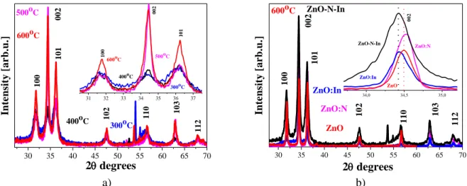
XRD patterns of ZnO:In:N films treated at temperatures ranging from 300 oC to 600 oC are presented in figure 1 (a). The film crystallization begins even at the lowest annealing temperature. The diffraction peaks observed correspond to a wurtzite phase (JCPDS 01-07-8070) without secondary phases. 30 35 40 45 50 55 60 65 70 112 103 110 102 101 002 100 600oC 500oC 400oC In te n si ty [ a r b .u .] 2degrees 300oC 31 32 33 34 35 36 37 101 002 100 600oC 500 oC 400oC 300oC 30 35 40 45 50 55 60 65 70 100 112 103 110 102 101 002 ZnO ZnO:In ZnO-N-In 600oC In te n si ty [ a r b .u .] 2degrees ZnO:N 34,0 34,5 35,0 002 ZnO ZnO:In ZnO-N-In ZnO:N a) b)
Figure 1. X-ray diffraction patterns of (a) ZnO:In:N films treated at different temperatures, and (b) comparison of ZnO, ZnO:N, ZnO:In and ZnO:In:N films annealed at 600 o
C.
The crystallization of the co-doped ZnO films is enhanced as the annealing temperature is increased. The ZnO-based films are polycrystalline after treatmet at 600 oC; however, a preferential orientation along the c-axis (the 002 peak has the highest intensity) is explicitly revealed for the ZnO:In and ZnO:In:N films.
The diffraction line is shifted from 34.497o (ZnO), to 34.506o (ZnO:N), to 34.447 o (ZnO:In); and for co-doped In, N-ZnO film, the line is at 34.413o. This is related to lattice strain caused by incorporating dopants atoms in the host lattice. The average crystallite sizes are estimated from the XRD peaks (100, 002 and 101 reflections) by using Scherrer’s formula; the determined lattice parameters are given in figure 2 b. The crystallites grow bigger as the annealing temperatures is raised up to 600 oC and strongly depend on the dopant used. It is seen that the crystallites of the ZnO:In:N films are the smallest. The lattice parameters of the ZnO:N films are somewhat different, especially for the annealing temperature of 400 oC.
21st International Summer School on Vacuum, Electron and Ion Technologies Journal of Physics: Conference Series 1492 (2020) 012027
IOP Publishing doi:10.1088/1742-6596/1492/1/012027 300 400 500 600 8 12 16 20 24 28 32 36 ZnO:N:In ZnO:In ZnO:N ZnO C r y st a ll it e s iz e [ n m ]
Annealing temperature [oC] 300 400 500 600
3,23 3,24 3,25 3,26 5,19 5,20 5,21 5,22 5,23 5,24 5,25 3,23 3,24 3,25 3,26 5,19 5,20 5,21 5,22 5,23 5,24 5,25 ZnO:In:N ZnO:In ZnO:N Annealing temperature [oC] a (Å) c (Å) ZnO a) b)
Figure 2. Dependence of the crystallite size (a) and the lattice parameters (b) on the annealing temperature.
The FTIR spectra of the studied sol-gel films treated at 300 oC and 600oC are presented in figure 3. Few absorption bands related to the OH stretching and bending vibrations at 3450 cm-1 and 1610 cm-1 are seen in the spectra of ZnO:In and ZnO:N:In films (not shown here). The OH species are present in the films with In content due to the higher OH adsorption energy on In-doped ZnO surfaces [6]. For single ZnO and ZnO:N films, there are almost no absorption features above 3000 cm-1. The IR lines at 2960 cm-1 and 2850 cm-1 are assigned to C-H stretching modes, while the absorption features at 2340 cm-1 are due to atmospheric CO2 (seen in all spectra) [7].
The main absorption band of the ZnO films shifts from 407 cm-1 to 395 cm-1 as the annealing temperature is raised, as seen in figure 3. The ZnO films possess an absorption band at 520 cm-1 for the sample annealed at 600 oC; it is known that the lines at 408 cm-1 and 513 cm-1 are theoretically assigned to wurtzite ZnO [8].
400 500 600 700 800 900 1000 ZnO:In ZnO ZnO:In:N T r a n sm it ta n c e [ a r b .u .] Wavenumber [cm-1] 300oC ZnO:N 400 500 600 700 800 900 1000 ZnO ZnO:In ZnO:N:In T r a n sm it ta n c e [ a r b .u .] Wavenumber [cm-1] 600oC ZnO:N a) b)
Figure 3. FTIR spectra of ZnO and doped ZnO films annealed at 300 o
C and 600 oC.
The nitrogen incorporation in ZnO can be expressed by modifying the absorption bands of hydroxyl group vibrations and the C-H, O-H and N-H bonds [9]. In our case, the ZnO:N films reveal strong and broad absorption features around 400 cm-1. The main band is split in two lines at 397 cm1 and 419 cm-1 for the film treated at 300 oC, the film treated at 600 oC exhibits one strong line at 407 cm-1. These bands are assigned to the Zn-O stretching vibrations [10]. The IR lines at 420 cm-1, 522 cm-1and 660 670 cm-1 are attributed to the stretching vibrations of Zn-O in a wurtzite structure [11]. Indium doping results in shifting and broadening of the main absorption bands, compared to
21st International Summer School on Vacuum, Electron and Ion Technologies Journal of Physics: Conference Series 1492 (2020) 012027
IOP Publishing doi:10.1088/1742-6596/1492/1/012027
4
those of the undoped ZnO and ZnO:N films. The characteristic vibrational modes of In2O3 are located at 609 cm-1, 540 cm-1, 429 cm-1 and 324 cm-1 (stretching modes) and a bending vibration at 847 cm-1 [8]. However, ZnO also possesses characteristical absorption features in this spectral range. The main IR lines are located at 405 cm-1 (for 300 oC temperature treatment) and at 420 cm-1 (600 oC) and are attributed to the stretching Zn-O mode. The FTIR spectra of ZnO:N:In films present strong and broad absorption bands at 402 cm-1 after treatment at 300 oC and 600 oC. The IR lines of the 300 oC-treated film are observed at 520 cm-1 and 488 cm-1, while the main absorption broad line is transformed into three bands at 446 cm-1, 426 cm-1 and 401 cm-1. These lines are related to the Zn-O vibrations [10]. The annealing at 600 oC provokes the appearance of new peaks at 672 cm-1and 653 cm-1 with a stronger and sharper main IR line. All IR lines are related to Zn-O vibrations, but the co-doping effect is observed in the changed shapes and positions of the absorption features. We thus conclude that nitrogen, indium and N, In incorporation affects the vibrational and structural properties of the ZnO films, but the wurtzite structure is maintained without secondary phases.
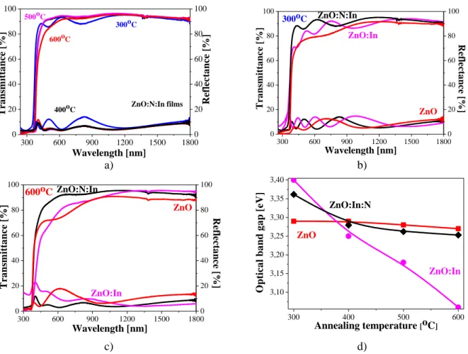
The transmittance and reflectance spectra of the sol-gel ZnO:In:N films are given in figure 4 a. The average transmission (T) and reflectance (R) of the co-doped ZnO films is 89,6 % and 8,3 % (300 oC), 92,9 % and 4,3 % (400 oC), 93,4 % and 4,8 % (500 oC) and 89,4 % and 5,0 % (600 oC), respectively, in the spectral range 450 900 nm. It is known that the ZnO films’s transmittance is closely related to the their surface morphology [12], homogeneous structure and crystallinity.
300 600 900 1200 1500 1800 0 20 40 60 80 100 0 20 40 60 80 100 600oC 500oC 400oC R e fl e c ta n c e [ % ] T r a n sm it ta n c e [ % ] Wavelength [nm] ZnO:N:In films 300oC 300 600 900 1200 1500 1800 0 20 40 60 80 100 0 20 40 60 80 100 ZnO ZnO:In R e fl e c ta n c e [ % ] T r a n sm it ta n c e [ % ] Wavelength [nm] 300oC ZnO:N:In a) b) 300 600 900 1200 1500 1800 0 20 40 60 80 100 0 20 40 60 80 100 ZnO ZnO:In R ef le ct a n ce [ % ] T ra n sm it ta n ce [ % ] Wavelength [nm] 600oC ZnO:N:In 300 400 500 600 3,10 3,15 3,20 3,25 3,30 3,35 3,40 ZnO:In:N ZnO:In ZnO O p ti c a l b a n d g a p [ e V ] Annealing temperature [oC] c) d)
Figure 4. Transmittance and reflectance spectra of a) ZnO:N:In films treated at different temperatures, b) and c) comparison of ZnO, ZnO:In and co-doped ZnO films annealed at 300 o
C and 600 oC, respectively, d) optical band gaps depending on the annealing temperature.
The high transparency of the ZnO:In:N films (around and above 90 %) implies a relatively compact and smooth surface that reduces light scattering. Figures 4 b and c present the transmittance and reflectance spectra of ZnO, ZnO:In and ZnO:In:N films. It can be seen that the co-doped ZnO:In:N films improve their optical transparency compared to the other films studied. The ZnO film has an
21st International Summer School on Vacuum, Electron and Ion Technologies Journal of Physics: Conference Series 1492 (2020) 012027
IOP Publishing doi:10.1088/1742-6596/1492/1/012027
average T = 80,6 % and R = 9,0 % (300 oC) and T = 77,9 % and R = 12,6 % (600 oC). The corresponding values for ZnO:In films are T = 86,0 % and R = 9,6 % (300 oC) and T = 9,3 % and R = 10,8 % (600 oC). The optical characterization reveals that the sol-gel ZnO-based films are highly transparent. Their transmittance is reduced after the annealing procedure at the highest temperature.
The dependence of the optical band gap (Eg) on the temperature treatment is presented in figure 4 d. The ZnO films show a slight change of the Eg values. The ZnO:In films exhibit a sharp decrease of the optical band gap with the rise of the annealing temperature. The commons tendency is of narrowing the optical band gap, with the exception of the sample annealed at 300 oC. A similar behavior is found for the ZnO:In:N films; however, the values differ. The changes in the optical band gap may be induced by various factors, including crystalline structure, stoichiometry, grain size, lattice parameters, defects, nature and concentration of impurities [13]. A narrowing of the optical band gaps has been reported for ZnO:In and ZnO: N films [14, 15]. It can be explained by the presence of defects induced by In and N doping in the ZnO host lattice.
4. Conclusions
Sol-gel technology was applied to depositing highly transparent and uniform thin films of nitrogen and indium co-doped ZnO films on different substrates. The ZnO:In:N films crystallize even after annealing at 300 oC in a wurtzite ZnO structure without other crystalline phases. The 002 diffraction line reveals a shift resulting from the doping, proving that In, N are successfully incorporated in the host lattice. The average crystallite size of the ZnO:In:N film is the smallest in comparison to the ZnO and ZnO:In films. The FTIR analysis also confirms that the N, In incorporation affects the vibrational and structural properties of the ZnO films without disrupting the wurtzite crystalline structure. Co-doping results in improved film transparency. The optical band gap is estimated and discussed. References
[1] You Q, Cai H, Hu Z, Liang P, Prucnal S, Zhou S, Sun J, Xu N and Wu J 2015 J. Alloys Comp. 644 528
[2] Kaur M, Kaur P, Kaur G, Dev K, Negi P and Sharma R 2018 Vacuum 155 689 [3] Kumar M, Kim S-K and Choi S-Y 2009 Appl. Surf. Sci. 256 1329
[4] Mallick A and Basak D 2018 Prog. Mater. Sci. 96 86
[5] Ivanova T, Harizanova A, Koutzarova T and Vetruyen B 2010 Mater. Lett. 64 1147
[6] Marikutsa A, Rumyantseva M, Gaskov A, Batuk M, Hadermann J, Sarmadian N, Saniz R, Portoens B and Lamoen P 2019 Fronties Mater. 6 art.43
[7] Gayathoie S, Ghosh O S N, Sathiskumar S, Sudhakara P, Jayaramudu J, Ray S S and Viswanath A K 2015 Appl. Sci. Lett. 1 8
[8] Yuvaraj D and Rao K N 2008 Vacuum 82 1274
[9] Keyes B M, Gedvilas L M, Li X and Coutts T J 2005 J. Crystal Growth 287 297 [10] Kumari R, Sahai A and Goswami N 2015 Prog. Nat. Sci.: Mater. Int. 25 300 [11] Zerdali M, Hanizaoui S, Teheran F H and Rogers P 2006 Mater. Lett. 60 504 [12] Yan W, Tan J, Zhang W, Meng X, Lei T, Li C and Sun X 2012 Mater. Lett. 87 28 [13] Girtan M, Socol M, Pattier B, Sylla M and Stanculescu A 2010 Thin Solid Films 519 573 [14] Bouaine A, Bourebia A, Guendouz H and Riane Z 2018 Optik 166 317