T
T
H
H
È
È
S
S
E
E
En vue de l'obtention du
D
D
O
O
C
C
T
T
O
O
R
R
A
A
T
T
D
D
E
E
L
L
’
’
U
U
N
N
I
I
V
V
E
E
R
R
S
S
I
I
T
T
É
É
D
D
E
E
T
T
O
O
U
U
L
L
O
O
U
U
S
S
E
E
Délivré par l'Université Toulouse III - Paul SabatierDiscipline ou spécialité : Electronique Moleculaire
Présentée et soutenue par
Ather Mahmood
Le 15 Juin 2009
Titre :
Towards Graphene based mono-molecular electronics:
Structural and electrical characterization of side-gated devices
JURY
Prof. Jean-Marc Broto Prof. Thomas Ebbesen
Dr. Annick Loiseau Dr. Paolo Samori Dr. Dominique Vuillaume Dr. Dimitri Roditchev Dr. Christian Joachim Dr. Erik Dujardin
Ecole doctorale : Ecole doctoral sciences de la matière
Unité de recherche : Centre d'Elaboration de Maté'riaux et d'Etudes Structurales Directeur(s) de Thèse : Christian Joachim, Erik Dujardin
Rapporteurs : Dr. Annick Loiseau
I am grateful to the director of CEMES, Dr. Jean-Pierre Launay, and the members of his secretariat, for providing me the opportunity to join the lab and helping me through all the administrative procedures required for the completion of the thesis.
My sincere thanks go to the thesis director and the group incharge, Dr Christian Joachim, who has been the source of inspiration throughout these years. It was within the early years of masters that the notion of mono-molecular electronics was introduced to me and perhaps remained an enigma for a long time.
It seems difficult to express my gratitude and thanks to Erik Dujardin for playing such an outstanding role in supervision of scientific matters and, sometimes, personal matters. He introduced me to the field of nanoscience and has guided my research from the first day at the AFM controls to the finer points of science. To him I owe my devotion to SPMs and all things “nano”. Throughout the thesis, I always enjoyed our long scientific sittings, which usually started from a specific question, gradually broadened into wider perspective, and finally ended only when it was too late to go home. I appreciate his encouragement and support of new ideas and am happy that I learned to do clean and careful experiments from him.
Many parts of this thesis would have remained incomplete without the collaboration of the group of Drs. Dominique Vuillaume, Thierry Mélin and Isabelle-Roch Jeunne at IEMN, Lille, and Drs. Marek Potemski, Duncan Maude and Clément Faugeras at GHMFL, Grenoble. Our group has collaborations with the two labs and I met these scientists/professors during meetings and conferences and benefited enormously from their expertise and knowledge.
During my time in CEMES, I constantly felt the support and encouragement from the members of the Group Nanosciences including Thierry Ondarçuhu, Sebastien Gauthier, David Martrou, André Gourdon, Xavier Boujou, Christian Girard, Christine Viala, and Mohammed Hliwa, to name a few. Surely, the colleagues within Erik’s team have direct or indirect contribution in my work. Among them, Jean-François Dayen joined as a post-doc in the second year of my PhD and we shared quite funny moments together. His replacement, Caterina Soldano, has also been helpful with valuable advices for writing the manuscript. Others, including Audrey Sanchot, Régis Diaz and Sebastien Linas joined the group at a later stage and I shared valuable moments with each one of them.
I would have never been able to accomplish this objective without the incessant support from my family and parents. During the months of writing of this manuscript, my wife Sarah, and children, Marusha and Mueen, endured my absence with patience, during evenings and over the week-ends. On the other hand, my parents remained a source of encouragement and patiently looked forward for my success during the last five years of my stay in France. I owe my thanks to their love, support and prayers for my success.
Finally, I am grateful for the financial support that I received as a scholarship from Higher Education Commission (HEC) of Pakistan. Most of the credit goes to the former chairman of HEC, Prof. Dr. Atta-ur-Rahman, who envisioned, obtained necessary funding, and chalked out a continued research program in a post-PhD scenario within the country.
Chapter 1 Introduction . . . 1
Chapter 2 Exploiting flat carbon sheets for mono-molecular electronics . 11 2.1 Scope of the chapter . . . 11
2.2 Molecular electronics . . . 14
2.2.1 Hybrid molecular electronics . . . 14
2.2.2 Establishing contact with molecules . . . . 15
2.2.3 Logic functions using hybrid molecular electronics . . 18
2.2.4 Open questions for hybrid molecular electronics . . 20
2.3 Mono-molecular electronics . . . 21
2.3.1 Complex logic functions using mono-molecular approach . 22 2.4 Electronic properties of graphene . . . 24
2.4.1 Band structure of graphene . . . 24
2.4.2 Electric field effect . . . 28
2.4.3 Other electronic properties . . . 30
2.5 Bilayer graphene . . . 33
2.6 Back to graphite . . . 35
2.7 Graphene nanoribbons . . . 36
2.7.1 Field effects on GNRs . . . 37
2.8 Epitaxial graphene . . . 38
2.9 Exploiting Graphene for mono-molecular electronics . . 39
2.9.1 Mono-molecular electronics revisited . . . 39
2.9.2 Suitability of graphene for MME . . . . 41
2.9.3 Proposed work . . . 43
Chapter 3 Preparation and characterization of graphene 57
3.0 Résumé du chapitre . . . 57
3.1 Scope of chapter . . . 59
3.2 Materials and methods . . . 59
3.2.1 Graphite sources . . . 59
3.2.2 Chemicals, solvents and gases . . . . 60
3.2.3 Instruments . . . 60
3.3 Thin graphitic microstructures and graphene monolayer . . 62
3.3.1 Deposition on substrates: parameters. . . . 62
3.3.2 Outline of proposed method for obtaining thin graphitic microstructures . . . 62
3.3.3 HOPG micro pillars . . . 64
3.3.4 Cantilever-borne graphite stamps . . . . 65
3.3.5 Direct manipulation and mechanical exfoliation . . 68
3.3.6 Manipulation on diverse substrates . . . . 70
3.3.7 Extension to other layered materials . . . . 71
3.4 Micromechanical exfoliation of graphite . . . . 73
3.5 Characterization of graphitic samples using scanning probes . 76 3.5.1 Structural characterization through AFM . . . 76
3.5.2 Estimating graphene substrate distance . . . 81
3.5.3 Revealing the interfacial layer . . . . 83
3.6 Other methods of characterization . . . 88
3.6.1 Signatures of Raman spectroscopy of graphene . . 88
3.6.2 Raman studies over exfoliated graphene and multilayered discs 91 3.7 Conclusion . . . 96
3.8 References . . . 97
Chapter 4 Electrical transport measurements of side-gated graphene devices 101 4.1 Introduction . . . 101
4.1.1 Objectives . . . 101
4.1.2 State of the art . . . 102
4.1.3 Challenges . . . 103
4.1.4 Strategies . . . 105
4.2.1 Principles of FIB . . . 106 4.2.2 Ion Sources, optics and detection . . . . 108
4.2.3 FIB milling . . . . . . 110
4.2.4 FIB induced deposition . . . 112 4.3 Electrical contacting of multi-layered graphene disks . . 113
4.3.1 FIB induced lithography . . . 114
4.3.2 Resist-free deposition of electrodes . . . . 117 4.3.3 Electrical characterization of FIB-deposited ohmic contacts 119
4.4 Tailoring graphene sheets by FIB lithography . . . 120 4.4.1 Characterization of graphite-ion interaction . . . 120
4.4.2 Device layout and fabrication . . . . 124
4.5 Field-effect cryotransport measurements . . . . 127
4.5.1 Variation of ribbon resistance . . . . 128
4.5.2 Side-gate dependency of I(V) characteristics . . 129 4.5.3 Model based on coulomb blockade . . . . 131 4.5.4 1-D array of tunnel junctions . . . 134
4.5.5 Recent experimental studies on nanoribbons . . 135
4.6 Conclusion and outlook . . . 140
4.7 Bibliography . . . 141
Chapter 5 Electrostatic Force Microscopy of graphene sheets and ribbons 147
5.1 Introduction and scope . . . 147
5.1.1 Charge distribution and screening in layered graphene:
an overview . . . 148
5.2 EFM: a brief introduction and its utility . . . . 150 5.3 Electrostatic variants of AFM modes . . . . 153
5.3.1 Kelvin probe microscopy . . . 153
5.3.2 Electrostatic force gradient . . . 156
5.3.3 EFM protocols for present study . . . . 157 5.4 EFM imaging of graphene on silicon/silica substrates . . 158
5.4.1 Experimental section . . . 158
5.4.2 EFM imaging of non-charged graphene islands . . 158 5.4.3 Influence of the silicon oxide thickness . . . 160 5.5 Surface potential of graphene and FLG . . . . 164
5.5.1 Experimental details . . . 164
5.5.2 Results and interpretation . . . 166
5.6 Quantitative analysis of injected charge densities . . . 169
5.6.1 Experimental protocol . . . 169
5.6.2 Abrupt discharge and charge evacuation . . . 170
5.6.3 Background information on surface charge density quantified by EFM . . . 172
5.6.4 Results and interpretation: Quantitative analysis of surface charge densities . . 173
5.6.5 Model and interpretation . . . 176
5.7 Charge delocalization in FLG transistor devices . . . 178
5.7.1 Device fabrication with AFM mechanical lithography . 179 5.7.2 Charge spread through FIB fabricated graphene constrictions 182 5.7.3 Side-gate effect for static charge . . . . 184
5.8 Conclusion . . . 188
5.9 Bibliography . . . 189
Chapter 6 Conclusion . . . 195
Introduction
La miniaturisation continue des dispositifs électroniques à base de silicium suit, depuis un demi-siècle, la loi de Moore selon laquelle le nombre de transistors par
unité de surface double tous les 18 mois
environ. Elle a conduit à des circuits toujours plus denses, plus rapides et plus efficaces. Mais, tandis que le motif
élémentaire approche de la taille critique de
22 nm, la poursuite des méthodes classiques
de l'industrie des semi-conducteurs doit faire face à de plus en plus de défis technologiques et fondamentaux. Plusieurs solutions alternatives sont proposées par l'International Technology Roadmap for
Semiconductors (ITRS) (1) soit pour stimuler des innovations supplémentaires de la
technologie conventionnelle dite
"complementary metal oxide semiconductor
(CMOS)", soit pour promouvoir la recherche de nouvelles technologies dans une vision post-CMOS de la microélectronique. Bien que les composants CMOS à effet de champ ont été considérablement améliorés ces
The continuous miniaturization or
'scaling' of silicon-based electronic devices, following the ubiquitous Moore's law, that holds that the number of transistors will
double approximately every eighteen
months, has led to denser, faster and more power efficient circuitry. But as device
features are pushed towards the sub-22-nm node, the conventional scaling methods of the semiconductor industry face increasing technological and fundamental challenges. Several solutions are proposed by the
International Technology Roadmap for
Semiconductors(1) (ITRS) for either boosting silicon workhorse in the conventional complementary metal oxide semiconductor (CMOS) technology, or
finding new technologies in 'beyond-CMOS' era. Although the CMOS field effect
approach has been improving steadily for the
last 5 decades(2), alternative strategies to
obviate size effects in silicon-based devices
are being explored and among them,
cinquante dernières années, (2) d'autres stratégies sont à l'étude pour pallier aux effets de taille dans les dispositifs nanométriques à base de silicium. Parmi
elles, les approches dite "bottom-up"
(ascendantes) basées sur des composés
moléculaires ont été considérées comme un
paradigme radicalement nouveau. En
particulier, une intégration réussie à l'échelle moléculaire offrirait un moyen considérable d'intégrer plus de puissance de calcul dans des circuits intégrés de taille
ultime. Cependant, le compromis de cette
deuxième voie est la nécessité de mettre au point (i) des architectures d'interconnexions
fiables de l'échelle macroscopique à la taille
moléculaire, c'est-à-dire typiquement 1 nm,
et (ii) de comprendre comment le calcul peut être effectué avec des molécules car il n'y a pas de raison particulière ni nécessité pour que les molécules se conforment au concept
CMOS, il leur suffirait de produire une
logique booléenne.
Dans ce scénario, l'accent est spécialement mis sur le développement de nouveaux dispositifs, de techniques de
lithographie, d'interconnexion et de
technologies de conditionnement. Parmi les solutions prometteuses à moyen terme une
des options, toujours dans l'option CMOS post-silicium, est l'introduction de
l'électronique à base de carbone. Du point
de vue des matériaux, les nanotubes de
have been considered as a radically new paradigm. In particular, molecular-scale electronics holds considerable appeal as a way to pack yet more computation power
into ultimately small integrated circuits. In
this regard, even the semiconductor
industry's ITRS calls for new approaches in computing and the integration of emerging technologies, including molecular
electronics, to make computational systems
with ever-shrinking device dimensions or
increased complexity. The trade-off, however, is the need to develop (i) reliable
interconnection architectures down to
molecular size, i.e. typically 1 nm, and (ii) to understand how computation can be performed with molecules since there is no specific reason for current CMOS framework
to be suitable with molecules.
In this far-fetched scenario, emphasis is specially laid on emerging devices, lithographic techniques, interconnection and packaging technologies, which will require new and improved properties. Among these
solutions one promising midterm option, still
within a post-silicon CMOS approach, is the
introduction of carbon-based electronics. From the material point of view, carbon
two-carbone (CNT) et le graphène sont les formes à une et deux dimensions du carbone
qui ont récemment émergées comme de bons
candidats pour une future électronique nanométrique. Les nanotubes mono-parois
(SWNTs) présentent des mobilités de porteurs de charges élevées, des densités de
courant dépassant 109A/cm² et, en transistor
à effet de champ, une pente sous le seuil proche de l'optimum (3-5). Mais les composants à nanotubes individuels ne
pourront sans doute pas trouver
d'applications du fait de leur faible courant
de sortie. La synthèse de nanotubes à propriétés électriques homogènes et le positionnement précis de transistors à
nanotubes individuels en circuits intégrés
reste un problème majeur (6). Quelques
études récentes ont démontré que l'utilisation
de faisceaux denses, parfaitement alignés de
SWNTs comme partie active de transistor à
film mince permettait de résoudre
partiellement la limitation en densité de
courant. Toutefois, une densité en nanotubes par micron dix fois supérieure est encore
nécessaire pour atteindre les performances
actuelles du silicium(7).
Le graphène a été l'objet essentiel de
ce travail de thèse et, dans le cadre de
l'électronique nanométrique, pourrait potentiellement s'affranchir des limitations
des nanotubes. Ce travail est une contribution à un nouveau domaine en
dimensional form of carbon, has recently emerged as a strong candidate for future
nanoelectronics. Single-walled carbon
nanotubes (SWNTs) show very high mobilities and current densities as high as
109A/cm² and ideal sub-threshold
characteristics(3-5). But single SWNT based devices might not be used as functional
elements due to their low current outputs and small active areas. Synthesizing electrically homogeneous tubes and accurately positioning single tube devices in scalable integrated circuits remains a very
challenging problem(6). A recent study has
demonstrated the use of densely packed, perfectly aligned horizontal arrays of non
-overlapping linear SWNTs as active thin
film electronic material, yet a ten-fold increase of the density is still required to meet current specifications of routine silicon
devices(7).
Graphene has been the centrestone of this thesis project and, in the course of it, has been revealed as potentially able to circumvent the CNT limitations. This work is a contribution to a quickly expanding new
expansion rapide de l'échelle nanométrique
électronique.
Le graphène est un feuillet
d'atomes de carbone hybridé sp² disposés, en
deux dimensions, suivant un réseau en nid
d'abeille. Bien que disposant d'une structure
atomique simple, le graphène est le siège
d'une physique complexe encore largement
inexplorée et fascinante. Il y a quatre ans seulement, il a été découvert que des feuillets de quelques voire une seule couche de graphène pouvaient être produits avec une facilité inattendue par exfoliation mécanique
du graphite au moyen d'un simple ruban
adhésif, ce qui a déclenché des recherches intenses au cours des quatre dernières
années(8,9). Les raisons de l'extraordinaire
intérêt pour le graphène est triple: (i) son
diagramme de bande particulier implique que ses porteurs sont bien décrits par
l'équation de Dirac plutôt que l'habituelle
équation de Schrödinger(10); (ii) son
épaisseur monoatomique pour une extension
latérale macroscopique lui confère une
morphologie plus facile à intégrer dans les
dispositifs que les CNT, donc plus adaptée
aux procédés technologiques connus (11);
(iii) les porteurs de charges peuvent être
confinés par la formation de rubans étroits, ce qui rend possible l'ingénierie de ses
propriétés électronique à l'échelle
nanométrique d'autant plus que les propriétés obtenues dépendront a priori très
Graphene refers to a sp² -bonded
sheet of carbon atoms arranged in a two-dimensional honey-comb lattice. Though possessing a simple atomic structure, graphene presents largely unexplored and yet
intriguingly complex physics. Recently, it
has been found that free-standing single or few layer sheets could be produced with unexpected ease by mechanical exfoliation of graphite, which triggered intensive
research efforts in the past four years. (8,9)
The reasons for the extraordinary interest in graphene are threefold: (i) its unusual electronic spectrum means that its carriers are well described by a version of the Dirac equation rather than the more usual
Schrödinger equation(10); (ii) its unique
one-atom thick yet macroscopic lateral extension
morphology rendering integration into
devices relatively easier than CNT, thus
more suitable for technological processes (11); (iii) electrons and holes can be further
confined by forming narrow ribbons, thus tailoring its nanoscale properties by opening
finement de la morphologie des rubans (12).
Du point de vue technologique, il est
important de réaliser que, si le graphène
possède des propriétés électroniques
comparables à celles des CNTs, il offre de
nombreuses possibilités de contourner les
limitations désormais bien identifiées des composants à CNT sur la voie de l'intégration tout en restant compatible avec
les technologies actuelles de lithographie. La
topologie bidimensionnelle du graphène
offre une occasion unique de réaliser des
motifs suffisamment petits pour pouvoir
intégrer, directement sur une seule et même feuille de graphène, plusieurs composants
actifs et passifs (13).
Ainsi, le graphène peut être considéré
comme un système mésoscopique π conjugué
qu'une structuration multi-échelle peut relier
à l'échelle moléculaire où les entités ultimes
sont des anneaux de benzène ou des chaines
d'atomes de carbones (14). Ces
caractéristiques répondent précisément aux
exigences du concept d'électronique mono-moléculaire qui propose une approche intra-moléculaire, selon laquelle des circuits et
dispositifs peuvent être intégrés dans une seule molécule. Cette approche repousse
toutes les interconnexions métalliques à l'échelle du micron alors que la molécule
exerce toutes les fonctions nanoscopiques. Dans ces conditions, le principal défi est alors l'identification des structures de
From the technological viewpoint, it is important to realize that apart from comparable electronic properties with CNTs, graphene has potential for circumventing many of the integration challenges faced by
CNT technology for fabrication of high mobility planar devices, compatible with the present day lithography technology. The 2-D expanse of graphene offers a unique opportunity where lithographic patterning at
a sufficiently small device feature size(13)
may be used to write device features directly onto a single sheet thus dividing it into active
and passive components, all incorporated
into the same sheet.
This meets precisely the idea of
mono-molecular electronics which proposes an intermolecular electronics concept, where circuits and devices may be integrated in a single molecule. This approach repels all
metallic interconnects at the micron scale while the molecule performs all nanoscopic functions from within. Ultimately structured
graphene can be considered as a mesoscopic
π-conjugated system connected to
molecular-scale features where the basic entities are
benzene rings.(14) However, the key challenge then becomes the identification of the graphene structures with geometries suitable for devices. New circuit rules and long range electron tunnelling effects have to be understood and mastered. The recent
graphène pertinentes pour réaliser des
dispositifs à calcul appropriés. De nouvelles règles de circuits électriques doivent être
comprises et rationalisées. Les progrès
rapides de ces dernières années dans le
contrôle de la découpe des rubans de graphène(15) et la compréhension des effets
de bord(16) et de la passivation des atomes
de carbone de bord indique que, tôt ou tard,
les techniques de lithographie seront
disponibles pour la réalisation dans une feuille de graphène de dispositif fonctionnels.
Tout en nous efforçant, au
cours de ce doctorat, de progresser vers cet
objectif ultime, nous avons développé des premières approches de la préparation du graphène, de la fabrication d'un premier
type de dispositif et de la caractérisation de
leurs propriétés électroniques comme preuve de principe de notre approche. Ces résultats sont décrits dans ce manuscrit. Par souci de clarté, le présent manuscrit a été divisé selon
le plan suivant.
Le Chapitre 2 aborde les concepts et
réalisations récentes qui sous-tendent l'électronique moléculaire. Le concept
d'électronique moléculaire hybride est présenté, qui repose sur l'interconnexion
d'entités moléculaires par des électrodes
métalliques afin de produire des dispositifs
rapid advances in controlling the size of
graphene ribbons(15) and understanding the
associated edge effects(16) and passivation of edge carbon atoms, is indicating that sooner or later lithography techniques will be
available for writing device functionalities
directly within a graphene sheet.
While striving to move towards this
ultimate goal in the course of this doctoral
work, we have taken the initial steps from
material preparation to proof-of-principle
device fabrication and characterization which are described in this manuscript. Electronic properties of graphene and fabrication of devices through scanning probe and ion-beam lithography, respectively, have been studied. For the purpose of clarity, the present manuscripthas been divided into chapters according to the
following scheme.
Chapter 2 discusses the concepts and recent developments underlying molecular electronics. The concept of hybrid molecular electronics is introduced that entails the
molecular entities being interconnected with metallic electrodes for complex device
fonctionnels complexes. L'électronique
mono-moléculaire est ensuite examinée en détail avec les principaux défis auxquels est
confronté sa mise en œuvre ainsi que les
récentes prédictions théoriques qui permettraient de surmonter certains d'entre
eux. Enfin, la structure électronique du
graphène est présentée. Tout en décrivant les propriétés spécifiques du graphène, un
accent particulier est mis sur celles qui ont
des conséquences directes sur la fabrication
et la caractérisation de dispositifs électroniques alors que le comportement dit
"relativiste" et les propriétés qui s'y
rattachent ne sont que brièvement
mentionnées.
Le Chapitre 3 détaille la préparation graphène et la caractérisation de ses propriétés structurales par sonde à balayage
et spectroscopie Raman. En particulier, la
méthodologie adoptée pour fabriquer les
plots micrométriques sur graphite
pyrolytique et la façon dont des disques
minces de graphite en ont été extraits par
micromanipulation puis déposés en un
endroit prédéfini entre les électrodes sont décrites. Enfin, la spectroscopie Raman a été
utilisée pour confirmer le nombre de couches
déterminé par les méthodes précédentes.
Au Chapitre 4, nous montrerons comment la lithographie à faisceau d'ions focalisé (Focused Ion Beam, FIB) peut être
then discussed in detail with the key challenges being faced for its implementation and the recent theoretical predictions to overcome some of them.
Finally, detailed description of graphene bandstructure and its implications are described. While describing the properties, a particular stress is laid on highlighting properties which have direct consequences on electronic device fabrication and
characterization, and only passing remarks
are given on relativistic and other properties.
Chapter 3 details the preparation of graphene and methodologies adopted to characterize the structural properties by scanning probe and Raman spectroscopy. In particular, the methodology adopted to fabricate micropillars on pyrolytic graphite
and the way thin discs were
micromanipulated and placed in between pre-defined electrodes are described. Finally, Raman spectroscopy has been used for
correlating the number of layers counting with that of data obtained from previous
methods.
In Chapter 4, we demonstrate how Focused ion Beam (FIB) lithography can be used to fully process graphene devices from
utilisée pour réaliser des dispositifs en graphène multicouche, depuis la fabrication
des contacts métalliques jusqu'à la nanostructuration du graphène avec une
résolution inférieure à 100 nm sans
contamination par les résines usuelles en
lithographie. Notre approche est illustrée par la fabrication de transistors en graphène
à double grilles latérales, ayant un canal de
2 µm de long et 80 - 250 nm de large. Les propriétés de transport des transistors graphitiques ont été étudiées en fonction de la largeur du canal, depuis la température
ambiante, jusqu'à 40 K. Les observations expérimentales ont été interprétées comme provenant d'une série 1-D de barrières
tunnel séparant des îlots de graphène le long du canal et un modèle simple rend bien
compte des caractéristiques I(V, T) .
Si FIB offre une voie potentielle à la fabrication de nanocomposants de graphène sans résine, elle ne permet pas de réaliser des contacts électriques de qualité avec le
graphène monocouche. Ainsi, nous
présentons, dans le Chapitre 5 une technique sans contact permettant de sonder des propriétés électroniques 2-D du feuillet et
des rubans graphène, à savoir la microscopie à force électrostatique (EFM).
Une pointe métallique EFM est utilisée
comme sonde à long distance des gradients
de champ électrique. Elle permet de déterminer le potentiel de surface et la
the fabrication of metallic contacts to the
sub-100 nm graphene nanopatterning without any resist contamination. Our
approach is exemplified with double side-gated all-graphene transistors with 2 µm long
and 80- 250 nm wide multi-layered graphene
channels. The gate-dependent charge transport properties through graphitic
channels of various widths were studied from ambient to low temperatures. The experimental observations were interpreted
and modelled as tunnelling through 1-D potential barriers formed within graphitic
channels.
While FIB offers a potential route to
device fabrication without resist, it suffers of
similar ion-damage related limitations as standard lithography approaches. Thus we
introduce, in Chapter 5 a contact-less
technique to probe the 2-D electronic properties of graphene sheets and ribbons,
namely Electrostatic Force Microscopy (EFM). EFM is used to probe the long range electric field gradients, determine the surface potential and the surface charge density of
the sample. By eliminating the tip-sample capacitive effects the surface potential of pristine graphene sheets ribbons, and the
densité surfacique de charge de
l'échantillon. En éliminant les effets
capacitifs entre la pointe et l'échantillon, le potentiel de surface des feuillets vierges de graphène, et la densité surfacique de charges injectées, ont été mesurés en fonction de
l'augmentation du nombre de couches de graphène. Les résultats de ces expériences
ont été appliqués à la caractérisation
statique de l'injection puis de la
délocalisation de charges dans des feuillets monocouches de graphène structurés en
transistor à double grille latérale comme au
Chapitre 4.
surface charge density of injected charge, were studied with respect to the increasing graphene layers. The experiences from this study were used to probe the static injected charge delocalization through graphene
channels of transistors having similar
Bibliography
1. Arden, W. (2006) Future semiconductor material requirements and innovations as projected in the ITRS 2005 roadmap. Materials Science and Engineering B-Solid State
Materials for Advanced Technology, 134, 104-108.
2. Schaller, R.R. (1997) Moore's Law: Past, present, and future. Ieee Spectrum, 34, 52-&. 3. Durkop, T., Getty, S.A., Cobas, E. and Fuhrer, M.S. (2004) Extraordinary mobility in
semiconducting carbon nanotubes. Nano Letters, 4, 35-39.
4. Yao, Z., Kane, C.L. and Dekker, C. (2000) High-Field Electrical Transport in Single-Wall Carbon Nanotubes. Physical Review Letters, 84, 2941 LP - 2944.
5. Zhou, X., Park, J.-Y., Huang, S., Liu, J. and McEuen, P.L. (2005) Band Structure, Phonon Scattering, and the Performance Limit of Single-Walled Carbon Nanotube Transistors. Physical Review Letters, 95, 146805.
6. Avouris, P., Chen, Z.H. and Perebeinos, V. (2007) Carbon-based electronics. Nature
Nanotechnology, 2, 605-615.
7. Kang, S.J., Kocabas, C., Ozel, T., Shim, M., Pimparkar, N., Alam, M.A., Rotkin, S.V. and Rogers, J.A. (2007) High-performance electronics using dense, perfectly aligned arrays of single-walled carbon nanotubes. Nature Nanotechnology, 2, 230-236.
8. Novoselov, K.S., Geim, A.K., Morozov, S.V., Jiang, D., Katsnelson, M.I., Grigorieva, I.V., Dubonos, S.V. and Firsov, A.A. (2005) Two-dimensional gas of massless Dirac fermions in graphene. Nature, 438, 197-200.
9. Novoselov, K.S., Geim, A.K., Morozov, S.V., Jiang, D., Zhang, Y., Dubonos, S.V., Grigorieva, I.V. and Firsov, A.A. (2004) Electric field effect in atomically thin carbon films. Science, 306, 666-669.
10. Semenoff, G.W. (1984) Condensed-Matter Simulation of a Three-Dimensional Anomaly. Physical Review Letters, 53, 2449 LP - 2452.
11. Geim, A.K. and Novoselov, K.S. (2007) The rise of graphene. Nature Materials, 6, 183-191.
12. Chen, Z.H., Lin, Y.M., Rooks, M.J. and Avouris, P. (2007) Graphene nano-ribbon electronics. Physica E-Low-Dimensional Systems & Nanostructures, 40, 228-232. 13. Ebbesen, T.W. and Hiura, H. (1995) Graphene in 3-Dimensions - Towards Graphite
Origami. Advanced Materials, 7, 582-586.
14. Chen, F. and Tao, N.J. (2009) Electron Transport in Single Molecules: From Benzene to Graphene doi:10.1021/ar800199a. Accounts of Chemical Research, 42, 429-438. 15. Han, M.Y., Ozyilmaz, B., Zhang, Y.B. and Kim, P. (2007) Energy band-gap
engineering of graphene nanoribbons. Physical Review Letters, 98.
16. Kobayashi, Y., Fukui, K., Enoki, T., Kusakabe, K. and Kaburagi, Y. (2005) Observation of zigzag and armchair edges of graphite using scanning tunneling microscopy and spectroscopy. Physical Review B, 71.
Exploiting flat carbon sheets for mono-molecular
electronics
2.1
Objectifs du chapitre
En soixante ans, l'électronique a maintenu sa suprématie sur le traitement de l'information grâce à une intégration
massive et continue des composants
élémentaires et des architectures de ses systèmes. Désormais, la taille minimale d'un composant de base, comme le transistor à effet de champ, approche le seuil de 10 nm en technologie CMOS. L'extrapolation naturelle vers des tailles plus petites encore
nous amène directement dans le domaine de l'électronique moléculaire, pour lequel des molécules, individuelles ou en petits ensembles, offrent la possibilité de traiter l'information à une plus petite échelle. Ce concept n'est pas apparu parce que
l'approche "top-down" dominante a atteint ses limites mais a été en fait proposé depuis plus de 30 ans.
Dans ce laps de temps, la
compréhension des processus électroniques
2.1
Scope of the chapter
In sixty years, electronics has been
maintaining its supremacy on information processing thanks to the tremendous and continuous improvement of integration and performance levels. As a consequence, the
minimal feature size is nearing the sub-10 nm range in CMOS technology. The
spontaneous extrapolation to yet smaller size meets the realm of molecular electronics, in which molecules, either individually or in
small ensembles, offer the opportunity to process information at a smaller scale. This concept did not appear because the dominant
"top-down" approach had reached its limits but was actually suggested more than 30
years ago.
In this time span, the understanding of electronic processes at the level of a few
au niveau d'un petit nombre de molécules a progressé régulièrement, tant sur le plan
théorique et des aspects expérimentaux. Les surfaces atomiquement planes peuvent être préparées, des molécules peuvent y être assemblées et accrochées, et donc des caractéristiques de transport électronique peuvent être mesurées sur une seule ou
quelques molécules. Toutefois, la
compréhension globale des propriétés
électroniques à l'échelle d'une seule molécule en est encore à ses débuts, et la conception de nouvelles molécules pour mieux contrôler le transport électronique à travers elles est uniquement guidée par quelques règles simples. Un aspect encore inexploré est la question du lien entre une simple fonction électronique tels que la conduction le long d'un fil ou la rectification du courant dans certaines petites molécules
qui peuvent réaliser, dans une certaine mesure, et le véritable traitement de l'information qui exige une capacité de
calcul. Comme les grands systèmes
moléculaires potentiellement capables de réaliser ces calculs sont encore hors de portée, les efforts de recherche, au cours des
dernières décennies, se sont tourné vers des structures intermédiaires, en particulier les nanotubes de carbone qui ont été incorporés dans divers composants. Bien que les nanotubes offrent une possibilité d'interfacer des espèces moléculaires, une autre forme
molecules has progressed steadily both on the theoretical and experimental aspects.
Atomically smooth substrate surfaces can be prepared, molecular species can be attached, organized transport characteristics is measured on single or few molecules. However, the generic understanding of electronic properties at the single molecule
level is still in its infancy. The design of new molecules for better controlling electronic transport through them is only guided by a few simple rules. One missing aspect is bridging the gap between a simple electronic function such as conducting, rectifying
which small molecules can, to a certain extent, achieve and actual information processing which requires calculation. Since
the larger molecular systems capable to
achieve such calculations are still out of
reach, research efforts in the past few
decades has turned towards intermediate species, particularly those made of carbon (e.g. nanotubes) which have been incorporated in different devices. While nanotubes offers some possibility of interfacing molecular species, another allotrope form of carbon could be more
allotrope de carbone pourrait être plus
adaptée: le graphène.
Ce chapitre comporte une
introduction brève et partielle de
l'électronique moléculaire. L'électronique moléculaire offre principalement deux perspectives à un traitement de l'information post-CMOS. La première, issue du paradigme proposé par Aviram et Ratner en 1974, propose de confier à une molécule individuelle le soin de moduler le transport
électronique. Elle remplit alors le rôle
"post-silicium" d'une diode, d'un fil voire d'un
transistor moléculaire pour une architecture
envisagée qui reste néanmoins
fondamentalement de type CMOS. La seconde, proposée en 1984 par F. Carter, suggère de s'affranchir des concepts de
l'architecture CMOS reposant sur
l'assemblage de transistors en portes
logiques elles-mêmes cascadées en fonctions supérieures capables de calculer, pour confier à un système moléculaire plus complexe le soin de réaliser en interne une fonction de calcul et d'interfaçage avec N entrées/sorties. Dans ce cas, la logique
booléenne serait conservée mais la topologie
moléculaire "post-CMOS" n'aurait aucune raison de ressembler à l'architecture des processeurs en silicium d'aujourd'hui.
La seconde moitié de ce chapitre est consacrée à la présentation des propriétés
électronique du graphène qui offrent peut
After a very succinct and partial introduction on some of the basic concepts underlying molecular electronics, this chapter compares two approaches, namely the hybrid
molecular and the mono-molecular
electronics to extract the salient features of the later concept for ultimate device
integration.
The second half of the chapter is dedicated to highlight the electronic
être une opportunité unique pour l'étude de composants et architectures nouvelles permettant un véritable traitement de
l'information à l'échelle moléculaire
properties of graphene which are relevant to
future molecular-scale electronic device
fabrication.
.
2.2
Molecular electronics
In this section we will present the concepts underlying molecular electronics and the many approaches adopted for their experimental realization.
The concept of device feature size reduction broadly falls under the domain of "top down" approach for miniaturization of electronic components. In 1960 Richard Feynman proposed the idea that no law in physics prohibits the assembly of individual atoms and molecules in order to realize calculating machines. The concept of molecular electronics appeared soon after, getting its major thrust after the birth of scanning tunneling microscopy, invented in 1980s. Later, Becker used it to modify the atomic surface of a germanium crystal[1]. Soon the manipulation of individual atoms on a surface, one by one, by the STM tip was demonstrated by D.M. Eigler[2] and this became the beginning of the approach called "bottom up" for fabricating nanostructures.
2.2.1 Hybrid molecular electronics
The first visionary device based on single organic molecule was a rectifier, proposed by Aviram and Ratner in 1974[3] and marked the birth of hybrid molecular electronics. This technology is called "hybrid since" a molecule is interconnected with metallic electrodes, as in CMOS circuits. The scheme presented the placement of a molecule consisting of an electron donor, connected to an electron acceptor via an "insulating" σ-electron organic bridge. Figure 2.1 displays the schematics of this concept along with the energy level diagram of its working. The built-in electronic asymmetry of the molecule may cause the rectification action: the two conjugated groups, acceptor and donor, have a strong electron affinity and weak ionization potentials, respectively. While the molecule is forward biased, the highest occupied molecular orbital, HOMO, of the donor is put into resonance with the lowest unoccupied molecular orbital, LUMO, which results into current flow. In the reverse bias, the
Figure 2.1: Aviram’s and Ratner’s molecular rectifier: (a) A donor-spacer-acceptor molecule is sandwiched between two electrodes. (b) Schematic of the electronic structure at zero bias. The Fermi-levels EF of the electrodes and the highest occupied and lowest unoccupied molecular orbital of the donor
and acceptor, HOMO and LUMO respectively, are depicted. (c) At sufficiently large negative bias at the acceptor electrode, electrons can tunnel from the donor’s HOMO to the electrode while the HOMO is refilled by electrons tunnelling through the LUMO of the acceptor. (d) At the same opposite bias no major tunnelling contributions can be expected due to the intrinsic asymmetry of the arrangement.
tunneling of the current is not possible due to the asymmetry of the molecule. This idea motivated numerous theoretical and experimental studies in the past 35 years that led to the development of several techniques to study electron transfer through the molecules to uncover electronic components as explained below.
2.2.2 Establishing contact with molecules
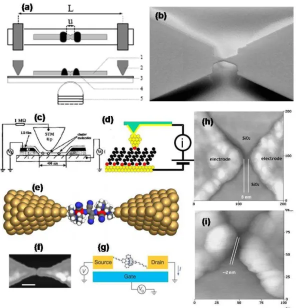
Several techniques have been used to approach and contact individual or ensembles of molecules; some of these contact methods are shown in Figure 2.2 and detailed below. Earliest techniques providing precision to fabricate molecular devices by film-forming molecules are Langmuir-Blodgett (LB) technique and self-assembled monolayer (SAM) fabrication method[4,5]. The former can be used to transfer amphiphilic molecules from water surface onto a solid substrate by slowly raising the substrate out of the water over which the film is spread. SAM fabrication method deals with monolayers of organic molecules chemically grafted on solid substrates. Two methods can then be used for studying the resulting monolayers: investigating long range tunneling through alkane chains or evaporating a second electrode on top. Some important results for device application include the observation of a current rectification[6,7] and the fabrication of molecular switches[8,9] based on LB films.
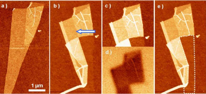
Figure 2.2: Various schemes of contacting molecules. (a) Schematics and (b) SEM image of a mechanically controllable break junction. (c) Contacting a Langmuir Blodget film through STM tip. (d) Alkane thiol adlayer with gold dot current collector measured using contact AFM. (e) Schematic structure of an MMM junction with a hypothetical conformation of the transition metal complex molecule represented in it. (f) SEM image of the realized experimental mesoscopic device[13] with the transistor configuration shown in (g). (h) and (i) AFM images of the narrow gap electrodes[14] fabricated through electron-beam lithography, show the distances of 8 and 2 nm, respectively.
A controlled addressing of single molecules is possible with STM which ensures contact with individual molecules[10-12] resulting also in two-terminal measurement (Figure2.2c). Examples include the electrical single-atom switching action using Xe[15] and first experimental realization of transistor based on C60 molecule[16,17]. However, the
measured resistance is of the metal-molecule-metal junction and not of the molecule itself; further the direct tunneling between tip and substrate is not uncommon in STM based studies. Similarly, the varying tip shapes from one experiment to the other render the contacts
asymmetric. The direct tunneling may arise from the gap between the STM tip and SAM surface thus rendering the estimation of true conductance dependant on careful data analysis and choice of experimental conditions[18]. New insights on the electronic properties of molecular junctions have been achieved through STM based break junctions, where STM tips can repeatedly make and break junctions with Au surface in a solution containing molecules of interest[19]. Statistical measurements of the conduction data have led to the analysis of the variability of conductance[19], role of metal-molecule chemical link[20], and on the influence of the atomic configuration of chemical link[21].
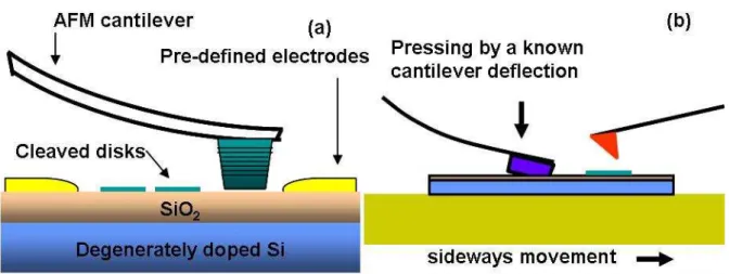
Conducting AFM (C-AFM) is an alternative for studying electron transport at the nanoscale where a metal probe will assist in taking topographical scans prior to establishing gentle mechanical contact[22,23] (Figure 2.2d). The advantage is a physical separation of tip-sample position control and current probing; this is different in the case of STM where same tunneling current controls the tip position and transport properties. However, an important consideration is the exertion of mechanical pressure on the molecules under study which might influence the electronic properties[24]. In certain cases this controlled pressure is an attribute where it can be used to change the molecular conformation and study its relationship with electronic properties[25].
An important technique for measuring molecular conduction between two metal electrodes in a planar geometry is Mechanically Controllable Break Junction (MCBJs) which was first introduced in 1990s for the molecular electronics studies[26-28]. A nanofabricated junction provides an electrode pair which is gently fractured by mechanical deformation by a piezoelectrically driven piston from below (Figure 2.2a). The gold wire breaks with two Au shards formed in between, with narrow gaps whose width is controllable to less than 0.1 nm by the piezo. The gap is atomically sharp, in which molecules are deposited by putting a drop of solution and letting the solvent evaporate. The pioneering measurements[26] revealed that the maximum conductance was that due to a single molecule (45 nS at 1V bias) which increased by a factor of 2 in case of two molecules. Although the configuration of interconnected molecules approaches the planar wiring, little knowledge of exact number and conformation of molecules is there for most of the cases. Very few experimental studies have been realized which target conduction through single (or a very few) molecules[27,29] with room temperature mechanical stability.
Other techniques have been used to determine electron transparency, including the experiments based on nanopore[30], electrodeposition[31], Coulomb blockade[32] and nanolithography[33]. It is difficult to determine the precise number of molecules trapped
Figure 2.3: Molecular scale devices: (a) A molecular rectifier constructed from donor (red), bridge (black), and acceptor (blue) components. (b) A single molecule transistor constructed from a symmetrical cobalt complex. S, source; D, drain; G, gate[34].
within the gaps and their exact conformation cannot be verified. However, molecular scale devices were realized (Figure 2.3) following the Aviram and Ratner's proposal: they ranged from rectifying diodes[6], molecular wires[35], and molecular memories for information storage[36].
2.2.3 Logic functions using hybrid molecular electronics
The progress in the last 30 years also furnished 3-terminal transistor devices[37-41] as being the key elements in the modern electronic architecture alloying switching and other logic operations. A molecular transistor design comprises of controlling the electron transfer rate through the molecule attached to metallic source-drain electrodes through the third external electrodes. This rate can be modified by the shift in energy of a given molecular level of the molecule, relative to the Fermi level of the electrodes, by the progressive closure of the HOMO-LUMO gap of the molecule or by a change of molecule/source and/or molecule-drain electronic coupling. Although not a molecule but a demonstration of transistor operation based on these principles involved a single walled carbon nanotube (SWCNT) FET device[42,43], which showed gain as function of its electronic structure (Figure 4b). Soon after, an implementation of a logic function involving voltage inverter operation was demonstrated where this logic function was performed using a chemically doped single nanotube bundle[44]. A conceptually different three-terminal device is the electromechanical amplifier based on C60 fullerene[17], where amplification was achieved by pressing with the
STM tip onto the buckyball (Figure 2.4c and d) which shifts and broadens its HUMO and LUMO and and increase the trannconductance to 3.9 µA/V.
Figure 2.4: A few proposed and realized molecular devices with three or more terminals. (a) Schematics of carbon nanotube transistors[43] are connected by gold interconnects to construct logic circuits. (b) Output voltage as a function of time for a nanotube ring oscillator. The three resistances are 100 megaohms, 100 megaohms, and 2 gigaohms[42]. (c) Electrical circuits of an electromechanical single C60 amplifier (in its
original scanning tunnelling microscope version[17]. (d) From (c), the transconductance dIdrain/dVgate of
the C60 amplifier is g = 3.9 X 10⁻⁶ A V-1. (e) Representative example of design of a hybrid molecular
electronic device. The figure shows the layout of a memory cell that consists of four individual C60
electromechanical transistors[45] (two for the trigger and two for the driving transistors) under a bias voltage VCC with respect to ground, GND. Inset, the equivalent electrical circuit diagram. b and b carry
the digital information to be stored in a memory cell, and the word line activates a line of memory cells for a storage operation.
The possibility of these devices being scalable to dimensions well below 50 nm and further, the demonstration of operation at a bandwidth of 10 THz implies an era of terahertz computing. This resulted into proposed study for interconnections of C60 electromechanical
transistors to form logic gates and memory cells[46] making use of its well-known equivalent circuit[45]. The operation of a class A amplifier, a NOT and NOR gate[46] and implementation of a static Random Access Memory (SRAM) (Figure 2.4e) has also been
demonstrated theoretically. This was explored in a hybrid technology as the electrodes/wires were not of the same material as the devices and the inter-device transport was not coherent. A hybrid molecular version of AND- and OR-gates was built by Heath and co-workers[47] where the wires were a few microns in section and redox-active molecules acting as diodes between them. By using the redox-properties of the molecule for reconfiguring, logic circuits and memories could be constructed.
2.2.4 Open questions for hybrid molecular electronics
Despite the immense progress in improving the techniques for measurement of single, few and ensembles of molecules in two-terminal electrode systems, probing the details of single molecule conductance has proven difficult. From the strategies available to overcome the problems of implementation of logic functions with molecules, one is termed hybrid molecular electronics where single molecule devices are interconnected by metallic electrodes[48]. However, the metallic interconnects and wires in hybrid devices are of mesoscopic dimensions with inter-device distances longer than the electron mean free path and phase coherence length[49]. As electrons tunnel through the molecule for rectification effects at each molecule-metal junction the transport through it is described in ballistic or tunneling regime. In contrast, the electron transport in metal wires can be described to lie in Boltzman regime[50] which is the case for CMOS technology thus posing difficulties for the compatibility in both regimes.
Furthermore, the technological realization of such structures necessitates scaling down of connections from the macroscopic contact pads, the microscopic wires interconnecting the active components to the placement of molecules in between them. Although this is a straight-forward and conventional approach as a concept, the recent work demonstrated that standard circuit laws, such as Kirchhoff laws, are not valid for wires shorter than 10 nm[51] since the transport regime is ballistic. This implies that, to conceive a complex circuit at room temperature, a minimum of 10-20 nm distance is always maintained between each molecular device for the quantum-to-classical conversion to be completed at the device level, device after device[52]. Thus, new intra-molecular circuit laws have been proposed[50], stressing the difficulties of a spatial extension of an intra-molecular circuit in order to support a complex digital logic circuit[52].
Apart from the device architecture design, the quest for new functions that can be performed by molecular scale devices is still on. Metal-molecule-metal junctions have shown non-linear transport characteristics but several questions remain unanswered as different
parameters of molecule/electrode interface influence the electron transport traversing the junction. These include geometrical aspects where the electrode-junction symmetry[53], the nature of metal-molecule contact[54], and the dimensions of the electrode[55], influence transport independently of the molecular structure.
Summarizing the above discussion, there exist many challenges in realizing such a circuit. First, for a complex logic circuit, it is well known that one needs devices with high gain in the circuit to maintain a good noise margin. Second, interconnections between the devices must be long enough to avoid quantification and coulomb blockade effects. For example, if the metallic interconnects are too short, locally the circuit becomes a succession of metal clusters separated by the molecules. Third, even a very clean parallel deposition process will lead to inaccuracies in positioning the molecules between junctions. Some junctions may even be found with no molecules at all. In a nutshell, functional nano-electronic circuits have to be dealt at the level of switches, interconnecting large number of devices at nanoscale and with external systems and design architecture for an easy communication with other systems[48].
2.3
Mono-molecular electronics
The problems faced with hybrid electronics approach will pose several difficulties in competing with current CMOS technology, although such devices can be designed in principle (Figure 2.5). Difficulties in realizing these devices will occur while scaling down such architectures at molecular level due to different transport regimes in metallic wires and molecules, where the later is based on the quantum transfer of electrons through a ballistic or tunneling molecular channel[52]. A conceptually comparable mono-molecular electronics (MME) approach was proposed in 1980s by F.L. Carter[56], where electronic function to be performed by the molecule is integrated with wiring into itself. The functions traditionally performed by wires, separators and the diodes are executed by the chemical groups attached to the molecule. Contrary to the hybrid approach where external leads provide electronic signals, these are provided elsewhere in the molecule. The molecule is made of functional chemical groups like molecular wires, intra-molecular switches and rectifiers etc., chemically bonded together to form single large molecules[48].
Figure 2.5: Original schematic drawing of a discrete single-molecule transistor. The valve action is supposed to be driven by the current intensity ig, with it the channel tunnelling current intensity. This
schematic shows the basic design behind all the molecular scale triode (or transistor) proposed today. It may be not appropriate at the nanoscale. An electromechanical effect for C60 or/and the electric field
effect for a single-wall nanotube are the only gating ‘extrinsic’ action actually working[57].
Theoretical considerations were later given[58] where it was assumed that the properties of composite molecule result as a superposition of its constituent parts. The detailed quantum mechanical computation of electron transfer shows that the π-conjugated ring provides alternative paths and the transfer rate of electrons is determined by quantum interference, one implication of which is the influence on electron transfer due to conformational changes. The experimental exploration of this approach[59] is based on bottom-up synthesizing complex molecules with well defined function and structure.
2.3.1 Complex logic functions using mono-molecular approach
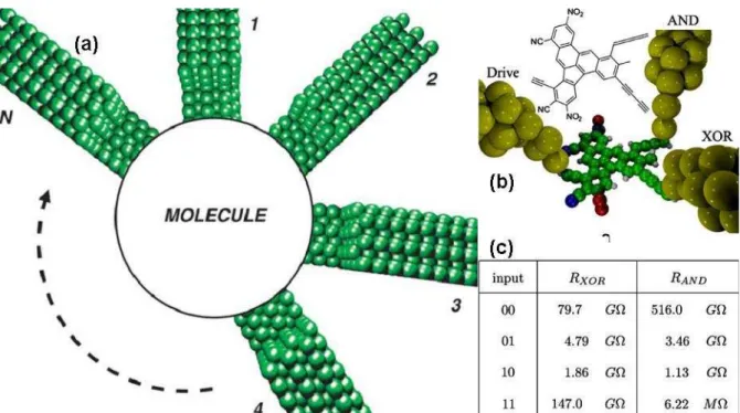
Contrary to the conventional electronic circuits, addition of new molecular wire or branch added to a molecule effectively results in creation of a 'new' molecule with a different electronic structure. As mentioned earlier, this condition renders the utility of standard circuit analysis laws inapplicable, which means that mesh Kirchoff's laws do not apply inside a molecule. Therefore a new intermolecular circuit simulator was used in studying the design of electronic logic functions (OR and AND) integrated inside a single molecule interconnected to the N-elecrodes[60] (Figure 2.6a). This simulator is called N-electrodes Elastic Scattering
Figure 2.6: (a) Structure of the scattering circuit made of a central molecule interacting with N electrodes. The full circuit is calculated with Extended Huckel Molecular Orbital EHMO–NESQC taking into account the EHMO valence molecular orbitals of the central molecule and the band structure of the electrodes in interaction with the molecule[60]. (b) The chemical structure of the molecule-1/2-adder with its dibenzo[a,e]fluoranthene CB skeleton and the nano-electrodes interconnects[61]. The conformation of each NO2 group encodes the logic input with a perpendicular conformation for a ‘0’ input and a planar
for a ‘1’. The output is encoded in the low voltage junction resistance between the drive and XOR (AND) nano-electrodes. A small resistance is encoding for a ‘1’. (c) The complete truth table for the XOR and the AND outputs. Notice the difference in magnitude between the XOR ‘1’ and the AND ‘1’.
Quantum Chemistry (N-ESQC)[62] working at the extended Huckel molecular orbital (EHMO) and can be thought of as a Simulation Program with Integrated Circuit Emphasis (SPICE) applicable at molecular level, permitting in obtaining its IV characteristics. ESQC was successfully used to study the scattering electronic properties of 4- electrodes and 2 electrodes mono-molecular Wheatstone bridges[50].
The 2-electrode mono-molecular Wheatstone bridge was theoretically considered more feasible than that of its 4-electrode counterpart, where the balancing of the bridge from inside the molecule is required using the central molecular branch as an intramolecular transducer detecting the electron transfer events inside the molecule.
Very recently, half adder logic function was suggested theoretically to work (Figure 2.6 b) in a single molecule (1/2 adder dinitro-anthracene), where the device architecture did not resemble CMOS[61] but that of a logic circuit configuration. The electron transparency of the molecule between three different leads is modulated and respect the truth table of an XOR and AND gate (Figure 2.6c).