HAL Id: tel-01763417
https://tel.archives-ouvertes.fr/tel-01763417
Submitted on 11 Apr 2018
HAL is a multi-disciplinary open access
archive for the deposit and dissemination of sci-entific research documents, whether they are pub-lished or not. The documents may come from teaching and research institutions in France or abroad, or from public or private research centers.
L’archive ouverte pluridisciplinaire HAL, est destinée au dépôt et à la diffusion de documents scientifiques de niveau recherche, publiés ou non, émanant des établissements d’enseignement et de recherche français ou étrangers, des laboratoires publics ou privés.
Thanyanan Phuphachong
To cite this version:
Thanyanan Phuphachong. Magneto-spectroscopy of Dirac matter : graphene and topological insula-tors. Materials Science [cond-mat.mtrl-sci]. Université Pierre et Marie Curie, 2017. English. �tel-01763417�
THESE DE DOCTORAT
DE L’UNIVERSITE PIERRE ET MARIE CURIE
Spécialité : Physique de la matière condensée
Ecole doctorale 397 Physique et Chimie des Matériaux
Réalisée au Laboratoire Pierre Aigrain
Département de Physique de l’Ecole Normale Supérieure
Magneto-spectroscopy of Dirac matter :
graphene and topological insulators
Présentée par
Thanyanan PHUPHACHONG
Pour obtenir le grade de
DOCTEUR DE L’UNIVERSITE PIERRE ET MARIE CURIE
Soutenue le 20 Septembre 2017
Devant le jury composé de :
M. Gwendal FEVE Président de jury
Mme Hélène BOUCHIAT Rapporteur
M. Frédéric TEPPE Rapporteur
M. Milan ORLITA Examinateur
Abstract
This thesis reports on the study under magnetic field of the electronic properties of relativistic-like Dirac fermions in two Dirac systems: graphene and topological insulators. Their analogies with high-energy physics and their potential applications have attracted great attention for fundamental research in condensed matter physics. The carriers in these two materials obey a Dirac Hamiltonian and the energy dispersion is analogous to that of the relativistic particles. The particle rest mass is related to the band gap of the Dirac material, with the Fermi velocity replacing the speed of light. Graphene has been considered as a “model system”, among quantum solids, that allows us to study the relativistic behavior of massless Dirac fermions satisfying a linear dispersion. When a Dirac system possesses a nonzero gap, we have massive Dirac fermions. Massless and massive Dirac fermions were studied in high-mobility multilayer epitaxial graphene and in topological crystalline insulators Pb1-xSnxSe and Pb1-xSnxTe. The
latter system is a new class of topological materials where the bulk states are insulating but the surface states are conducting. This particular aspect results from the inversion of the lowest conduction and highest valence bulk bands having different parities, leading to a topological phase transition. Infrared magneto-spectroscopy is an ideal technique to probe these zero-gap or narrow gap materials since it provides quantitative information about the bulk parameters via the Landau quantization of the electron states. In particular, the topological phase transition can be characterized by a direct measurement of the topological index.
Keywords:Dirac fermions, graphene, topological crystalline insulator, topological phase
transition, magneto-spectroscopy, Landau quantization.
Résumé
Ce travail consiste en l’étude sous champ magnétique des propriétés électroniques des fermions de Dirac relativistes dans deux systèmes: graphène et isolants topologiques. Leur analogie avec la physique des hautes énergies et leurs applications potentielles ont suscité récemment de nombreux travaux. Les états électroniques sont donnés par un Hamiltonien de Dirac et la dispersion est analogue à celle des particules relativistes. La masse au repos est liée au gap du matériau avec une vitesse de Fermi remplaçant la vitesse de la lumière. Le graphène a été considéré comme un « système école » qui nous permet d’étudier le comportement relativiste des fermions de Dirac sans masse satisfaisant une dispersion linéaire. Quand un système de Dirac possède un gap non nul, nous avons des fermions de Dirac massifs. Les fermions de Dirac sans masse et massifs ont été étudiés dans le graphène épitaxié et les isolants topologiques cristallins Pb1-xSnxSe et Pb1-xSnxTe. Ces derniers systèmes sont une nouvelle classe de matériaux
topologiques où les états de bulk sont isolants mais les états de surface sont conducteurs. Cet aspect particulier résulte de l’inversion des bandes de conduction et de valence du bulk ayant des parités différentes, conduisant à une transition de phase topologique. La magnéto-spectroscopie infrarouge est une technique idéale pour sonder ces matériaux de petit gap car elle fournit des informations quantitatives sur les paramètres du bulk via la quantification de Landau des états électroniques. En particulier, la transition de phase topologique est caractérisée par une mesure directe de l’indice topologique.
Mots clés: fermions de Dirac, graphène, isolants topologiques cristallins, transition de
Acknowledgements
First and foremost, I would like to begin by acknowledging the members of my thesis committee: Gwendal Fève, Hélène Bouchiat, Frédéric Teppe, and Milan Orlita. I thank them for taking the time out of their works and busy schedules to read this manuscript and participate in the thesis defense. I am extremely grateful to Frédéric and Milan who traveled very early in the morning from Montpellier and Grenoble to Paris, respectively, for being present at the thesis defense.
Secondly, my heart-felt thanks go to all the members (Yves Guldner, Louis-Anne de Vaulchier, Badih A. Assaf, and Gauthier Krizman) of the infrared and terahertz magneto-spectroscopy group at Laboratoire Pierre Aigrain (LPA), Department of Physics, Ecole Normale Supérieure, in Paris, France. Without their support, this work would not have been accomplished with extraordinary satisfaction that it was.
The first important person is Yves Guldner, my thesis supervisor, who provided me numerous great opportunities to do research on a fascinating topic in condensed matter physics. I thank him for his patience to supervise me and useful advice he gave me during three and a half years, since my master internship. He is a role model for hard work and determination. He showed me how to grow as a scientist, as a professional, as a teacher and as a person. He is more than a supervisor! I respect him as my grandfather and I feel always happy to go to work because this group is my second home.
The second one is Louis-Anne de Vaulchier, my thesis co-supervisor, who dedicated his time at the beginning of my research to teach me how the experimental setup works. He constantly encouraged me when experiments failed. He occasionally taught me some French slang words and phrases during our discussions or helium transfer. However, my academic French is usually corrected by his attention. It was amusing to spend time with him apart from physics discussion to discover French cultures and share Thai traditions. Most importantly, he always listens to me when I need to talk and never leaves my side in the most difficult times. This is the reason why I respect him as my father. His remarkably generous support is one of essential factors which brings me success.
The third one is Badih A. Assaf, postdoctoral fellow - Junior Research Chair at Ecole Normale Supérieure, who spent much time with me in the topological crystalline
to his remarkable characteristics. He is extremely active, always motivated by new interesting things in his research area, and enthusiastic about puzzling topics in physics. Most importantly, he always has positive attitude to overcome any problem encountered. I learned a lot from him how to bring out my potential to do my best in order to reach any goal.
The last one is Gauthier Krizman who joined the group for his master internship. He is very nice, generous, and disciplined. With his strong academic background in physics and mathematics, I am sure that he will move forward the research of the group and will be successful in his Ph.D. thesis.
Thirdly, I would like to convey my sincere gratitude to all the principle collaborators in France and in Austria who have prepared high-quality Dirac matter samples allowing me to accomplish this thesis.
Paola Atkinson and Mahmoud Eddrief from Institut des Nanosciences de Paris (INSP) fabricated thin films of Bi2Se3 topological insulator.
Abdelkarim Ouerghi from Laboratoire de Photonique et de Nanostructures (LPN), at Marcoussis, not far from Paris, prepared high-quality multilayer epitaxial graphene. Günther Bauer, Valentine Volobuev and Gunther Springholz from Johannes Kepler
University (JKU) Linz, in Austria, fabricated high-quality films of Pb1-xSnxSe and
Pb1-xSnxTe topological crystalline insulators.
I would also like to show my appreciation to the following individuals, working at Ecole Normale Supérieure, for their help and support.
Olivier Andrieu and Florent Perrin from cryogenic service of LPA prepared liquid helium for all the experiments carried out at low temperatures.
Anne Matignon, Olga Hodges, Fabienne Renia, Cécile Margossian, Alina Corches, Julie Loussier and Marie Chayla from administration team facilitated my administrative documents.
Pascal Morfin and Jules Silembo from technical service constructed and repaired experimental setup and essential equipment of the group.
I thank Juliette Mangeney for the opportunity she gave me to work with her team and Robson Ferreira for the theoretical explanations of my experimental results of graphene.
I especially thank Ph
.
D.
students (Sylvain Massabeau, Rémi Bisognin, Valentino Pistore, Holger Graef, Danijela Markovic, and Christophe Raynaud), postdoctoral fellows (Federico Valmorra and Hanond Nong), and young doctors (Ombline Lafont, Sarah Houver, Adrien Jeantet, Arthur Marguerite, Andreas Inhofer, Laure Bruhat, and Feihu Wang) for their help and friendship, and I also thank all the members of Ecole Normale Supérieure that I could not put their names on this page.In addition, I would also like to thank my friends in Paris, in Europe and in Thailand for their help, strong friendship and spiritual support.
French friends from Université Pierre et Marie Curie (UPMC Paris VI) since 2009 who taught me how to take notes, study, and write scientific reports in French style: Tabatha Sauvaget, Suzanne Dang, Myriam Rollat, Marina Vannier, Lucas Grosset, and Abderrezak Torche.
Thai friends in Paris who hung out, chilled out and strolled out in Paris with me: Suwanna Dolparadorn, Kantika Lohawiboonkij, Saroch Leedumrongwatthanakul, Nathassidh Comson, Theera Rungtheera, Teerawat Kulsuwan, Yotsakorn Klaewkla, Arinch Tanunkat, andPossathorn Sriya.
France alumni/Thai students in Europe/Mahidol Wittayanusorn friends/Buriram friends. In completing this independent study with the foremost success, I could not have accomplished this work without financial support and spiritual support from the following organizations.
“Mahidol Wittayanusorn” scholarship of Thai government which financially supported my whole life during memorable period (almost ten years) in France.
“Franco-Thai” scholarship of French government which financially supported my studies in doctoral degree and my accommodation during my last three years in France.
Office of the Education Council, Royal Thai Embassy in Paris, which took care of me about ten years in France.
The last three important people of my life to thank are 1st LTN Sekson Somnam and my beloved parents. I thank the first one for his encouragement and driving force he gave me to write this manuscript, and his spiritual support in tough periods during the last year in France. Last but not least, I would like to thank my beloved parents, Mr. Wattanai Phuphachong and
France, when I was just an eighteen-year-old girl, to study physics during a really long period. This chance allows me to discover Europe, and to gain very precious and unforgettable experiences.
Again, I would like to express that I am very grateful to have had received encouragement and supports from all of these individuals whose names are written down above, including some not mentioned here. Without them, I would not have been able to accomplish this solid work the way I have.
Vouloir, c’est pouvoir
.
List of abbreviations
Acronym
Definition
AFM atomic force microscopy
ARPES angle-resolved photoemission spectroscopy
BHZ Bernevig-Hughes-Zhang
BZ Brillouin zone
CR cyclotron resonance
CVD chemical vapor deposition
DFT density functional theory
FCC face-centered-cubic
FIR far-infrared
FIR-MT far-infrared magneto-transmission FTIR Fourier transform infrared interferometer
IQHE integer quantum Hall effect
IR infrared
LL Landau level
MBE molecular beam epitaxy
MDC momentum distribution curve
MEG multilayer epitaxial graphene
NEXAFS near-edge X-ray absorption fine structure
PMMA Poly(methyl methacrylate)
QAHE quantum anomalous Hall effect
QSHE quantum spin Hall effect
RHEED reflection high energy electron diffraction STEM scanning tunneling electron microscopy
STI strong topological insulator
STM scanning tunneling microscope
SWM Slonczewski-Weiss-McClure
TCI topological crystalline insulator
TI topological insulator
TKNN Thouless-Kohmoto-Nightingale-Nijs
TSS topological surface states
UHV ultra-high vacuum
VTI variable temperature insert
WTI weak topological insulator
XPS X-ray photoelectron spectroscopy
XRD X-ray diffraction
Contents
Introduction
1
Chapter 1 – Investigation techniques of Dirac matter:
ARPES and IR magneto-spectroscopy
5
1. Angle-resolved photoemission spectroscopy (ARPES) 7
2. Magneto-optical absorption spectroscopy 11
2.1. Sample preparation for measurement 12
2.1.1. Sample probe 12
2.1.2. Sample holder 13
2.1.3. Bolometer 14
2.2. Fourier transform infrared (FTIR) interferometer 14
2.2.1. Operating principle of the FTIR interferometer 14 2.2.2. Infrared light sources 16 2.3. Cryostat and superconducting coil 17
2.4. Data acquisition 18
References 21
Chapter 2 – Magneto-optics in multilayer epitaxial graphene
23
1. Electronic properties of graphene 25
1.1. Ideal graphene 26
1.2. Bilayer graphene 30
1.3. Trilayer graphene 32
1.4. Multilayer graphene 35
2. Fabrication methods of graphene 36
2.1. Mechanical exfoliation 36
2.2. Chemical exfoliation 37
2.3. Chemical vapor deposition 38
3. Magneto-spectroscopy in graphene 41 3.1. Ideal graphene 41 3.2. Bilayer graphene 44 3.3. Trilayer graphene 45 4. Experimental results 46
4.1. C-terminated face multilayer epitaxial graphene 46
4.1.1. Fabrication of C-terminated MEG samples 46 4.1.2. Dirac Landau level spectroscopy in monolayer and bilayer
graphenes 47
4.1.3. Disorder effect on magneto-optical transitions 53 4.2. Si-terminated face multilayer epitaxial graphene 58
4.2.1. Fabrication of Si-terminated MEG samples 58 4.2.2. Electronic band structure of trilayer graphene from ARPES
experiment 59
4.2.3. Infrared magneto-transmission results of trilayer graphene 62
5. Conclusion 64
References 67
Chapter 3 – A brief overview of topological matter
71
1. Topological insulators 73
1.1. Historical overview 73
1.1.1. Quantum Hall effect 73
1.1.2. Quantum spin Hall effect 76 1.2. Theoretical notions of topological states of matter 77
1.2.1. Berry phase 78
1.2.2. Topological invariants 79 1.3. Theoretical prediction and experimental realization of
Z2 topological insulators 81
1.3.1. 2D topological insulator: QSHE in CdTe/HgTe/CdTe
quantum wells 82
1.3.2. 3D topological insulator: Bi-based compounds 84
2. Topological crystalline insulators 89
2.1. Crystal structure 90
2.2. Band inversion 90
2.3. Topological surface Dirac cones in different bulk Brillouin zone
2.4. Electronic band structure of Pb1-xSnxSe and Pb1-xSnxTe 94
2.4.1. Electronic band structure of nontrivial Pb1-xSnxTe alloy 95
2.4.2. Electronic band structure of nontrivial Pb1-xSnxSe alloy 97
2.5. Valley anisotropy 100
3. Bernevig-Hughes-Zhang Hamiltonian for topological matter 102
References 105
Chapter 4 – Magneto-optical investigation of topological crystalline
insulators: IV-VI compounds
109
1. Dirac Landau levels of IV-VI semiconductors 111
1.1. Landau levels of the longitudinal valley 111
1.2. Landau levels of the oblique valleys 116
1.3. Landau levels of the topological surface states 116
2. Growth and characterization of (111) Pb1-xSnxSe and
Pb1-xSnxTe epilayers 117
2.1. Molecular beam epitaxy growth 117
2.2. X-ray diffraction 118
2.3. Electrical transport characterization 119
3. Magneto-optical Landau level spectroscopy of Dirac fermions
in (111) Pb1-xSnxSe 121
3.1. Bulk states in (111) Pb1-xSnxSe 121
3.2. Topological surface states in (111) Pb1-xSnxSe 131
4. Magneto-optical Landau level spectroscopy of Dirac fermions
in (111) Pb1-xSnxTe 133
4.1. Bulk states in (111) Pb1-xSnxTe 133
4.2. Topological surface states in (111) Pb1-xSnxTe 142
5. Magneto-optical determination of a topological index 145
5.1. (111) Pb1-xSnxSe 146
5.2. (111) Pb1-xSnxTe 149
6. Validity of the massive Dirac approximation 151
7.1. Pb1-xSnxSe 154
7.2. Pb1-xSnxTe 155
8. Absence of the band gap closure across the topological phase transition
in Pb1-xSnxTe 157
9. Conclusion and perspectives 159
References 162
Conclusion and outlook
165
Introduction
This thesis focuses on the magneto-optical study of the electronic properties of Dirac fermions and their relativistic behavior in two extensively studied Dirac materials: graphene (Nobel Prize 2010) and topological insulators (Nobel Prize 2016). Such materials have recently become of great interest in solid state physics owing to their analogies with high-energy physics and their potential for promising technological applications.
The first Dirac system studied in this work is graphene known as the first truly two-dimensional crystal, composed of carbon atoms, ever found in nature. In condensed matter physics, graphene has been considered as "the model system" for studying the behavior of relativistic-like electrons known as massless Dirac fermions owing to its gapless and linearly dispersing electronic band structure at low energies. These massless Dirac particles in the vicinity of the corners of the hexagonal Brillouin zone of graphene (Dirac cone) can be described by a Dirac Hamiltonian with a Fermi velocity 300 times smaller than the speed of light.
Recently, the search for other solid systems of which the carriers exhibit relativistic-like properties as those in graphene has become very active. Topological insulator is a new class of materials that provides access to the description of both relativistic massless and massive Dirac fermions. Note that the energy dispersion of massive Dirac fermions resembles that of graphene but there exists a mass term corresponding to the energy gap of the material. A notable characteristic of such material is that its bulk insulating states are coexisting with its surface conducting states occurring at the boundaries of the solid. This intriguing particular aspect originates directly from the spin-orbit coupling which invert the lowest conduction and the highest valence bulk bands of the material. The band inversion results in linearly dispersing spin-momentum locked topological surface states which are protected by time-reversal symmetry.
Such a physical phenomenon can be observed in narrow gap semiconductors where the role of the spin-orbit interaction is important enough to invert the bulk band ordering. The topological nature of condensed materials is thus fundamentally governed by the parity and orbital ordering of the conduction and valence bands. The material is in the trivial regime when the bands are normal (with positive band gap) and is in the nontrivial regime when the bands are inverted (with negative band gap). The material musts undergo a topological phase transition for changing the band ordering from trivial phase to nontrivial phase.
Another novel class of topological matter, so-called topological crystalline insulator, has been shown to display similar bulk and topological surface state properties as in the case of topological insulator, but the topological surface states are protected by the crystalline symmetry of the system. Narrow gap rocksalt IV-VI semiconductors such as Pb1-xSnxSe and Pb1-xSnxTe
were demonstrated to exhibit these topological properties. In this thesis, we chose these lead-tin chalcogenides as the second Dirac system to study the relativistic behavior of their massless and massive Dirac fermions, owing to their mirror-like conduction and valence bands. The topological phase transition resulting from the bulk band inversion can be studied by tuning the chemical Sn composition. For a given temperature, there exists a critical Sn content xc at which
the topological phase transition occurs in Pb1-xSnxSe and Pb1-xSnxTe. For x < xc, the system is
trivial and has a positive gap, while it is nontrivial and has a negative gap when x > xc.
In this work, magneto-optical absorption spectroscopy in the infrared domain (4-930 meV) is the principal technique used to investigate these zero gap (graphene) and narrow gap (topological crystalline insulators) semiconductors having the energy gap less than 1 eV.When a magnetic field is applied perpendicular to the crystal surface, the electron states are quantized into Landau levels. Optical transitions between Landau levels can be observed at the minima of the transmission spectra. This allows us to extract the band parameters, i.e. the Dirac mass or the energy gap and the Dirac velocity, of the material using the Dirac fermion model analysis. The obtained physical quantities of the bulk bands allow us to study the bulk band inversion or equivalently the topological phase transition of the topological system, making magneto-spectroscopy an ideal tool for probing topological material. Additionally, magneto-transport experiment, presented in the Appendix, can also be used as a technique to examine the topological character of a topological material via its bulk properties. Moreover, transport technique was used by M. König et al. in 2007 to demonstrate the quantum spin Hall effect in Hg1-xCdxTe/HgTe quantum wells, classified later as the first two-dimensional topological
insulator.
The present thesis is organized in two major parts, dealing successively with two Dirac matter systems: graphene and topological crystalline insulators. The magneto-optical study of relativistic-like Dirac fermions accommodated in these two quantum materials will be presented in this manuscript as follows:
1. The first chapter presents two investigation techniques that can be used to study the electronic properties of Dirac fermions: angle-resolved photoemission spectroscopy (ARPES) and IR magneto-optical absorption measurement. ARPES is a surface sensitive probe, while magneto-spectroscopy is essentially a bulk sensitive probe. The latter is the principal technique employed to realize this work and it allows us to investigate not only the bulk states, but also the surface states of solid materials.
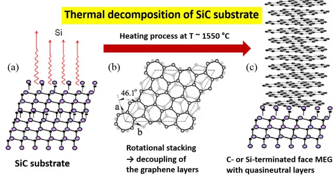
2. The second chapter is completely devoted to graphene. The electronic properties of single-layer graphene and graphene stacks (bilayer, trilayer, and multilayer) will be introduced. Several methods of graphene fabrication will be briefly described. The Landau quantization, in the presence of an external magnetic field, of the energy of Dirac fermions in different types of graphene stacking will be given. Magneto-optical results were mainly obtained from high-quality multilayer epitaxial graphene prepared by thermal decomposition of SiC substrates on both the C- and Si-terminated surfaces.
3. The third chapter briefly overviews the characteristic aspects of topological matter: topological insulators and topological crystalline insulators. The first section regarding topological insulators starts with historical overview, then theoretical notions of topological states of matter, and finishes with presenting some well-known two-dimensional and three-dimensional Z2 topological
insulators. We then describe topological crystalline insulator in the second section. This new kind of topological matter consists of narrow gap rocksalt IV-VI semiconductors such as Pb1-xSnxSe and Pb1-xSnxTe alloys. The
electronic band structure of different surface orientations and the valley anisotropy in both systems will be described in details. This facilitates the interpretation of the transmission spectra shown in the upcoming chapter. The last section shows a Bernevig-Hughes-Zhang Hamiltonian model, equivalent to a three-dimensional Dirac Hamiltonian, that can be used to describe the topological nature of relativistic-like massive Dirac fermions in both topological insulators and topological crystalline insulators.
4. The heart of this thesis is presented in the last chapter. This chapter shows the magneto-optical experimental findings of high-quality (111)-oriented Pb 1-xSnxSe and Pb1-xSnxTe films grown on BaF2 substrates by molecular beam
epitaxy. A systematic study, using Dirac Landau level magneto-spectroscopy, of the topological character of these chemical tuning systems across the topological phase transition is presented in details. From the bulk band parameters extracted, the valley anisotropy in Pb1-xSnxSe and Pb1-xSnxTe can
be studied in the vicinity of the topological phase transition. The most important aspect of our analysis is the ability to verify whether a material is trivial or nontrivial via its topological index that can be measured experimentally by magneto-spectroscopy. This important result demonstrates that the topological character of the material can be directly determined via the bulk properties.
5. Finally, we will conclude the ensemble of main results presented in this thesis and confirm that magneto-spectroscopy is a powerful investigation technique for Dirac matter. We will also give a few perspectives for future magneto-optical studies of the topological phase transition in various Dirac systems that can be described by a Bernevig-Hughes-Zhang Hamiltonian.
6. Another approach to determine the topological character via the bulk band properties of solids is represented in the Appendix. Performing magneto-transport experiment, high-quality (111) Pb1-xSnxSe epilayers were
demonstrated to exhibit the topological phase transition when the negative longitudinal magnetoresistance is observed and the system is in the nontrivial regime. The origin of this phenomenon will be described.
Chapter 1
Investigation techniques of Dirac matter:
ARPES and IR magneto-spectroscopy
Numerous investigation techniques are efficient to study the electronic band structure of quantum solids. In this chapter, we present two representative techniques used to probe Dirac fermions and allowing us to study the band dispersion in Dirac matter. The first one is the angle-resolved photoemission spectroscopy which allows a direct experimental study of the electron distribution in the reciprocal space. It is a surface sensitive probe for the electron surface states. The second one, which is essentially a bulk sensitive probe, is the magneto-optical spectroscopy in the infrared domain. We will show in the Chapter 4 that this technique can be used to probe not only the bulk states, but also the surface states of solid materials.
Chapter 1 - Investigation techniques of Dirac matter: ARPES and
IR magneto-spectroscopy
1. Angle-resolved photoemission spectroscopy (ARPES)
7
2. Magneto-optical absorption spectroscopy
11
2.1. Sample preparation for measurement 12
2.1.1. Sample probe 12
2.1.2. Sample holder 13
2.1.3. Bolometer 14
2.2. Fourier transform infrared (FTIR) interferometer 14
2.2.1. Operating principle of the FTIR interferometer 14 2.2.2. Infrared light sources 16
2.3. Cryostat and superconducting coil 17
2.4. Data acquisition 18
References
21
1. Angle-resolved photoemission spectroscopy (ARPES)
Angle-resolved photoemission spectroscopy (ARPES) is one of the photoelectron spectroscopy techniques based on the photoelectric effect first observed by H. Hertz 1 and later explained by A. Einstein for the quantum description of light 2. In other words, this technique relies fundamentally on the detection of photoemitted electrons allowing to probe directly the momentum-dependent electronic band structure and provide detailed information about the band dispersion and Fermi surface of solids. To obtain ARPES spectra, the kinetic energy and angular distribution of the electrons photoemitted from a material under sufficiently high-energy illumination are measured and analyzed. Up to now, ARPES reaches 2 meV high-energy resolution and 0.2° angular resolution 3 which lead to better reveal the behavior of the electrons
propagating inside a material through a penetration length of a few nanometers. This improvement has played a key role in enhancing the potential of ARPES to become a more sophisticated precision tool for the investigation of complex phenomena.
As mentioned earlier, the fundamental objective of an ARPES experiment is to detect the photoemission from the photoelectric effect occurring in a material. Within the non-interacting electron scheme and the energy conservation law, one can thus relate the kinetic energy (𝐸𝐸𝑘𝑘𝑘𝑘𝑘𝑘) of the photoelectron in vacuum to the binding energy (𝐸𝐸𝐵𝐵) of the electronic state inside the material by the following expression:
𝐸𝐸𝑘𝑘𝑘𝑘𝑘𝑘= ℎ𝜈𝜈 − 𝜙𝜙 − ǀ𝐸𝐸𝐵𝐵ǀ (1.1)
where ℎ is the Planck constant, 𝜈𝜈 is the photon frequency, and 𝜙𝜙 is the material work function. The latter represents the potential barrier at the surface that prohibits the valence electrons from escaping.
Fig. 1.1 schematically illustrates the photoemission occurring in a sample using ARPES probe under ultra-high vacuum (UHV) condition (𝑃𝑃 < 4 × 10-11 mbar) in order to minimize surface contamination and maximize the mean free path of the emitted electrons 3. A monochromatized light beam of energy ℎ𝜈𝜈 is incident on the sample. Light sources of energy between 10 and 200 eV are, for example, plasma helium discharge lamp, synchrotron radiation, or lasers. As a consequence, the electrons will be emitted by photoelectric effect and escape in all directions in vacuum. The hemispherical electron energy analyzer is employed to collect the photoelectrons (denoted as e- in Fig. 1.1). Such photoelectrons are directed onto a 2D multi-channel plate. The kinetic energy 𝐸𝐸𝑘𝑘𝑘𝑘𝑘𝑘 of the photoemitted electrons can then be measured for a given emission direction specified by the azimuthal (𝜑𝜑) and polar (𝜃𝜃) angles.
Figure 1.1. Photoemission geometry of an ARPES experiment. The incident photon of energy hν
causes the photoemitted electron (e-) escaping from the sample in vacuum. The emission direction of the photoelectron is identified by the azimuthal (𝜑𝜑) and polar (𝜃𝜃) angles. An electron energy analyzer collects the photoelectrons.
The wave vector or momentum of the photoelectrons in vacuum can be determined as 𝐾𝐾��⃗ = 𝑝𝑝⃗/ħ and its modulus is equal to 𝐾𝐾 = �2𝑚𝑚0𝐸𝐸𝑘𝑘𝑘𝑘𝑘𝑘/ħ, where ħ is the reduced Planck constant and 𝑚𝑚0 is the electron rest mass. The components parallel (𝐾𝐾��⃗∥ = 𝐾𝐾��⃗𝑥𝑥+ 𝐾𝐾��⃗𝑦𝑦) and perpendicular (𝐾𝐾��⃗⊥= 𝐾𝐾��⃗𝑧𝑧) to the sample surface can be obtained in terms of the emission angles (𝜑𝜑 and 𝜃𝜃) defined in
Fig. 1.1 as follows:
𝐾𝐾𝑥𝑥 =1ħ�2𝑚𝑚0𝐸𝐸𝑘𝑘𝑘𝑘𝑘𝑘sin(𝜃𝜃)cos(𝜑𝜑) (1.2a)
𝐾𝐾𝑦𝑦 = 1ħ�2𝑚𝑚0𝐸𝐸𝑘𝑘𝑘𝑘𝑘𝑘sin(𝜃𝜃)sin(𝜑𝜑) (1.2b)
𝐾𝐾𝑧𝑧= 1ħ�2𝑚𝑚0𝐸𝐸𝑘𝑘𝑘𝑘𝑘𝑘cos(𝜃𝜃) (1.2c)
Since the objective of ARPES measurement is to construct the electronic dispersion relation between the binding energy 𝐸𝐸𝐵𝐵 and the wave vector or momentum 𝑘𝑘�⃗ of the electrons propagating inside the material, we have to determine the two components of 𝑘𝑘�⃗ which are 𝑘𝑘�⃗∥ and 𝑘𝑘�⃗⊥. Here 𝑘𝑘�⃗∥ = 𝑘𝑘�⃗𝑥𝑥+ 𝑘𝑘�⃗𝑦𝑦 is the component parallel to the material surface while 𝑘𝑘�⃗⊥ = 𝑘𝑘�⃗𝑧𝑧 is the component perpendicular to the material surface. Note that ARPES measurement requires sufficiently clean surfaces in order to establish a definite relationship between the crystal wave vector (𝑘𝑘�⃗) and the measured wave vector (𝐾𝐾��⃗) of the extracted photoelectron. 𝑘𝑘�⃗∥ is conserved in the process. For a pristine sample, 𝑘𝑘∥ reads:
𝑘𝑘∥ = 𝐾𝐾∥= 1ħ�2𝑚𝑚0𝐸𝐸𝑘𝑘𝑘𝑘𝑘𝑘sin(𝜃𝜃) (1.3)
Contrary to 𝑘𝑘�⃗∥, 𝑘𝑘�⃗⊥ is not conserved but is necessary to map the electronic band structure. To calculate 𝑘𝑘⊥, we can adopt a nearly-free-electron description for the final bulk Bloch states 4.
We thus get: 𝐸𝐸𝑘𝑘𝑘𝑘𝑘𝑘+ 𝜙𝜙 =ħ 2𝑘𝑘�⃗2 2𝑚𝑚0 − |𝐸𝐸0| = ħ2(𝑘𝑘�⃗ ∥ 2+𝑘𝑘�⃗ ⊥2) 2𝑚𝑚0 − |𝐸𝐸0| (1.4)
Here, 𝐸𝐸0 corresponds to the energy at the bottom of the band with respect to the Fermi energy. As we can calculate the value of 𝑘𝑘�⃗∥2 from Eq. 1.3, the expression of 𝑘𝑘⊥ can thus be written as:
𝑘𝑘⊥ =1ħ�2𝑚𝑚0(𝐸𝐸𝑘𝑘𝑘𝑘𝑘𝑘𝑐𝑐𝑐𝑐𝑐𝑐2(𝜃𝜃) + 𝑉𝑉0) (1.5)
where the inner potential 𝑉𝑉0 = |𝐸𝐸0| + 𝜙𝜙 represents the energy of the bottom of the band referenced to the vacuum level.
The electronic band structure of a material can be established by studying the momentum-dependent binding energy (𝐸𝐸𝐵𝐵(𝑘𝑘�⃗ )). Only occupied electronic states can be observed by ARPES. Fig. 1.2 represents ARPES spectra obtained from different Dirac systems accommodating 2D and 3D topological Dirac fermions. These ARPES data clearly show the surface electronic structure dispersion map for the 2D topological surface Dirac cone in 3D topological insulator Bi2Se3 5, 3D tunable topological insulators TlBi(S1-xSex)2 with x = 0.5 6
and (Bi1-xInx)2Se3 with x = 0.04 7, and the 3D bulk Dirac cone in 3D Dirac semimetal Cd3As2 8. Moreover, ARPES measurement allows us to estimate the surface state band velocity from
Figure 1.2. ARPES measurements in different Dirac systems. ARPES spectra show the surface
electronic band structure of (a) 3D topological Dirac semimetal Cd3As28, (b) 3D topological insulators Bi2Se3 5, (c) TlBi(S0.5Se0.5)26 and (d) (Bi0.96In0.04)2Se37 in topologically nontrivial phase. Modified from 8.
In summary, ARPES is an ideal surface sensitive probe used to investigate the electronic band structure of quantum materials due to the improvements of energy and angle resolutions and data acquisition efficiency. There are also many exciting developments trying to add new dimensions into this technique leading to the spin-resolved ARPES and time-resolved ARPES. With the efforts put into its development, this powerful tool will continue playing an irreplaceable role in the search for novel phenomena of complex materials. The ARPES results that will be presented later in this work were obtained by our collaborators.
2. Magneto-optical absorption spectroscopy
In the previous section, ARPES as surface sensitive probe is shown to be a powerful tool allowing us to study the electronic band structure of Dirac materials. In this section, infrared magneto-optical absorption spectroscopy, the technique we used in this thesis to probe and characterize Dirac matter, will be described. When the crystal surface is subjected perpendicular to an applied magnetic field 𝐵𝐵, the electron states will be quantized into relativistic Landau levels dispersing as √𝐵𝐵 or �𝛼𝛼2+ 𝛽𝛽𝐵𝐵, where 𝛼𝛼 and 𝛽𝛽 are band parameters. This is a typical characteristic feature of Dirac fermions. The optical transitions occurring between these Landau levels give important information about the physical parameters of the electronic band structure of bulk states as well as surface states. Infrared spectral range is chosen thanks to the energy compatibility for probing semiconductors of which the energy gap is less than 1 eV. This is the primary reason why magneto-optical absorption spectroscopy in the infrared domain is primarily used in this thesis to investigate Dirac matter.
Fig. 1.3 shows the whole experimental setup used to probe Dirac fermions. The principal element is the Oxford Instruments 1.5K/17T cryostat, situated at the center of the photo, equipped with a superconducting coil. It allows us to do experiments in the temperature range 1.5 K < 𝑇𝑇 < 220 K and under magnetic fields 𝐵𝐵 = 0-17 T. The Fourier transform infrared (FTIR) interferometer (Bruker VERTEX 80V), located in the upper left hand corner of the photo, is employed as the infrared light source and the spectral analysis apparatus at the same time. These two essential elements are connected by a coupler containing a parabolic mirror. Detailed information about the experimental setup and the data acquisition will be described in the following subsections.
2.1. Sample preparation for measurement
Samples are first prepared and attached at the bottom of the sample probe for magneto-optical absorption measurement. In this subsection, three important parts will be described: the sample probe, the sample holder and the bolometer used as a detector of transmitted signals.
2.1.1. Sample probe
Figure 1.4. Different parts of the sample probe. (a) The sample is placed at the bottom of the sample
probe for measurement. The sample probe envelope is used to avoid any contact between the sample and the exterior environment. (b) Zoom of the top of the sample probe.
A 1.5 m long sample probe was designed to mount samples for magneto-optical absorption measurement and to maintain three electrical channels carried by two nonmagnetic coaxial cables (Fig. 1.4(b)). The inner walls of the sample probe guide the incident infrared light reaching towards the sample. The three channels are used for the ±18 V bolometer power supply, the signal acquisition of the bolometer and the ground. The sample probe envelope (Fig. 12
1.4(a)) is necessary for protecting the cables, the bolometer and the sample from the exterior environment when the sample probe is immersed in the cryostat filled with liquid helium. After the sample is mounted and sealed, the sample probe is primarily evacuated down to ~ 1 × 10⁻²
mbar. It is then filled with helium exchange gas, up to a pressure of 80-800 mbar at room temperature to ensure sample thermalisation, before being put into the variable temperature insert (VTI) of the cryostat for measurement. The pressure in the sample probe is maintained owing to a diamond window located at the connection between the sample probe and the coupler. The diamond window enables also an optimal passage of the transmitted signals throughout the infrared range. For the investigation of Dirac fermions in graphene and topological insulators, the pressure of the helium exchange gas is about 100-120 mbar at room temperature.
2.1.2. Sample holder
Fig. 1.5(a) shows two kinds of sample holders: sample holder with one hole and rotating sample holder with two holes. The sample holder used for the transmission experiment has several diameters. An appropriate diameter for a given sample is chosen for maximizing the transmitted signals. Fig. 1.5(b) shows a sample bonded on a sample holder. The rotating sample holder can mount two pieces of samples as seen in Fig. 1.5(c). The rotating system (Fig. 1.4(b)) joining the rotating sample holder allows switching from one sample to another sample in situ. This is very practical for a measurement requiring a normalization between two consecutive transmission spectra at the same applied field. To glue a sample on a sample holder, we use silver paste or PMMA (Poly(methyl methacrylate)).
Figure 1.5. Examples of sample holders. (a) Examples of a sample holder (with one hole) and a rotating
sample holder (with two holes). There are several diameters adapting to the dimension of the sample. (b) A sample glued with silver paste to the sample holder. (c) A sample and a substrate glued with silver paste to the rotating sample holder.
2.1.3. Bolometer
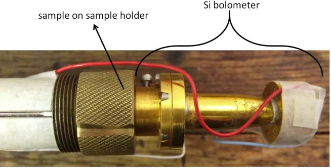
Figure 1.6. Infrared Si-composite bolometer with a diamond window. The Si bolometer and the
sample are attached to the bottom of the sample probe.
The bolometer is a photo-detector used for spectrum measurement. Its operating principle is to convert the energy of the incident electromagnetic radiation on the surface of a metallic or semiconductor absorber into heat. A Si-composite bolometer (Infrared Laboratories) equipped with a diamond window was used in this thesis for infrared magneto-optical absorption measurement. It is used to collect the transmitted light directly below the sample (Fig. 1.6). The signal from the bolometer passes through an external preamplifier before being transmitted to the FTIR interferometer for analysis. It is possible to adjust the amplification factor (200, 2,000 and 5,000) of the preamplifier to obtain satisfying signal intensity.
2.2. Fourier transform infrared (FTIR) interferometer
Infrared magneto-optical spectroscopy is a technique employed to obtain transmission spectra of a sample (intensity as a function of energy) in the infrared domain (30-7500 cm-1 or 4-930 meV). The laboratory is equipped with a Bruker VERTEX 80V Fourier transform infrared (FTIR) interferometer monitored by the OPUS operating software. This spectrometer plays two essential roles as infrared light source and spectral analysis tool.
2.2.1. Operating principle of the FTIR interferometer
As represented in Fig. 1.7, The FTIR interferometer possesses two infrared light sources: far-infrared (FIR) source for 30-700 cm-1 and mid-infrared (MIR) source for 700-7500
cm-1. The light beam is collimated and directed towards a beam splitter and a system of 14
associated mirrors. The half portion of the signal is transmitted to a mobile mirror which can move on nitrogen cushion thanks to a motor. When the mirror moves, each wavelength is periodically blocked or transmitted by the interferometer by interference phenomenon. Finally, the light emerging from the spectrometer is sent towards the cryostat using a vacuum coupler with a parabolic mirror. The incident light is then focused on the sample placed above the bolometer. The detector measures the light intensity remaining after passing through the sample and sends the transmitted signal, after amplification, to the FTIR interferometer for spectral analysis.
Figure 1.7. Schematic representation of the FTIR interferometer (Bruker VERTEX 80V).
The FTIR interferometer obtains the signal from the bolometer as an interferogram (the transmitted light as a function of mobile mirror position) (Fig. 1.8) and then changes it into a spectrum (the transmitted light as a function of energy) using the calculation of the Fourier transform (Eq. 1.6). Here, 𝐷𝐷(𝛿𝛿) is the intensity of the interferogram as a function of phase difference proportional to the mobile mirror displacement 𝛿𝛿. 𝐼𝐼(𝜈𝜈) refers to the intensity of the spectrum as a function of frequency 𝜈𝜈.
Figure 1.8. OPUS control window showing an interferogram. The central peak corresponds to the
zero path difference (ZPD) position of the mobile mirror at which the maximum of light passes through the interferometer towards the detector.
In order to get a good signal/noise ratio, each final spectrum is obtained after acquisition and average of several spectra. The number of averaged spectra is proportional to a parameter which is the number of scans. It can typically be selected among the values of 64, 128 or 256 scans. Furthermore, the maximal spectral resolution can be adjusted up to 0.2 cm-1. The spectral
resolution chosen for our magneto-optical absorption experiment is 5 cm-1. Note that the vacuum is essential during the measurement in the FTIR interferometer, the entire optical path and inside the coupler in order to avoid the absorption of the infrared light beam by the atmospheric gases (H2O, O2, CO2, etc.).
2.2.2. Infrared light sources
The typical characteristics of FIR and MIR light sources of the FTIR interferometer are summarized in Table 1.1.
Characteristics Far-infrared (FIR)
Mid-infrared (MIR)
Source mercury vapor lamp SiC rod heated to 𝑇𝑇 > 100 ℃
Beam splitter Mylar-Multilayer (CsI) KBr
Filter polyethylene diaphragm of adjustable diameter
Wavenumber range 30-700 cm-1 700-7500 cm-1
Wavelength range 14-333 μm 1.3-14 μm
Energy range 4-87 meV 87-930 meV
Table 1.1. Characterictics of FIR and MIR light sources.
The operating software OPUS represents a spectrum in a function of wavenumber 𝜎𝜎. Some useful formulas regarding the conversion between the energy 𝐸𝐸, the wavelength 𝜆𝜆, the wavenumber 𝜎𝜎 and the frequency 𝜈𝜈 are written in Table 1.2.
Energy (𝑬𝑬) Wavelength (𝝀𝝀) Frequency (𝝂𝝂)
𝐸𝐸(𝐽𝐽) =𝜆𝜆(𝑚𝑚) ℎ𝑐𝑐 𝜆𝜆(𝑚𝑚) =𝜎𝜎(𝑚𝑚1−1) 𝜈𝜈(𝐻𝐻𝐻𝐻) = 𝐸𝐸(𝐽𝐽)ℎ 𝐸𝐸(𝑚𝑚𝑚𝑚𝑉𝑉) = 𝜆𝜆(𝑐𝑐𝑚𝑚) × 10ℎ𝑐𝑐 × 1000−2× 1.6 × 10−19 = 𝜆𝜆(𝑐𝑐𝑚𝑚) 0.124 𝜆𝜆(𝜇𝜇𝑚𝑚) = 𝜎𝜎(𝑐𝑐𝑚𝑚10000−1) 𝜈𝜈(𝑇𝑇𝐻𝐻𝐻𝐻) = 𝐸𝐸(𝑚𝑚𝑚𝑚𝑉𝑉) × 10ℎ × 10−3× 1.6 × 1012 −19 =𝐸𝐸(𝑚𝑚𝑚𝑚𝑉𝑉)4.1
Table 1.2. Conversion formulas between 𝑬𝑬, 𝝀𝝀, 𝝈𝝈 and 𝝂𝝂.
Here, ℎ is the Planck constant (ℎ = 6.626 × 10⁻³⁴ J.s) and 𝑐𝑐 is the speed of light in vacuum (𝑐𝑐 =
2.997 × 10⁸ m/s).
2.3. Cryostat and superconducting coil
As illustrated in Fig. 1.9(a), the cryogenic storage dewar of total volume of 85 L contains a superconducting coil at the bottom of the cryostat and a variable temperature insert (VTI), resulting finally in a capacity of 46 L of liquid helium. The VTI is separated from the exterior container by the inner vacuum shield, consequently, the temperature of the sample can be varied to be different from the temperature of liquid helium (4.2 K). To decrease the temperature below 4.2 K, we introduce liquid helium from the exterior container into the VTI via the needle valve and then pump out the pressure in the VTI. To increase the temperature above 4.2 K, we use the Oxford Instruments ITC503 automated control/heater apparatus that allows us to fix the
superconducting coil as seen in Fig. 1.9(b). The sample holder is surrounded by the sample probe envelope to avoid any direct contact between the sample and liquid helium. The control and power supply of the superconducting coil are provided by the Oxford Instruments IPS120-10 apparatus, enabling to work at fixed magnetic fields and to sweep the field with a maximum speed of 1 T/minute.
Figure 1.9. Schematics of the cryostat equipped with a superconducting coil.(a) The dewar consists of two containers: an interior one or the variable temperature insert (VTI) and an exterior one containing the superconducting coil immersed in liquid helium. The maximum and minimum filling levels of liquid helium are indicated. The opening of the needle valve lets flow liquid helium from the exterior container into the VTI. (b) Zoom of the superconducting coil and the bottom of the sample probe. The heat exchange between the sample and the VTI is via a helium exchange gas of a pressure of 80-800 mbar at room temperature.
2.4. Data acquisition
In this thesis, all experimental results were obtained from infrared magneto-optical absorption measurement. Fig. 1.10 displays the whole experimental setup used to probe Dirac fermions in graphene and topological insulators. The process of spectra acquisition is as follows.The infrared light beam generated from FIR or MIR sources passes by the beam splitter and the system of associated mirrors in the vacuum FTIR interferometer and is then transmitted to the entrance of the sample probe using the vacuum coupler. The parabolic mirror inside the coupler bends the light beam to propagate directly to the sample placed at the center of the superconducting coil. The magnetic field is oriented perpendicular to the sample surface in Faraday geometry and can be varied up to 𝐵𝐵 = 17 T. Each measurement is performed at a constant magnetic field. The temperature is fixed at 4.5 K. The Si bolometer detects the transmitted light directly below the sample. The transmission signals are acquired, then amplified and sent to the FTIR interferometer for spectral analysis. The corresponding 18
interferogram is obtained after the analysis and will then be converted by Fourier transform calculation to the transmission spectrum.
The transmission spectra measured at different magnetic fields will be manipulated in order to obtain and analyze the relative transmission and the transmittance. As a result, we are able to extract valuable quantitative information about the physical properties, for instance, the Dirac velocity, the Dirac mass or the energy gap of a Dirac material. The relative transmission is defined to be the normalization of the sample transmission at a given magnetic field 𝑇𝑇(𝐵𝐵) by a zero-field sample transmission 𝑇𝑇(0). This indicates the absorption due to the transitions of carriers between different Landau levels.The transmittance at a fixed magnetic field is defined as the sample transmission 𝑇𝑇𝑐𝑐𝑇𝑇𝑚𝑚(𝐵𝐵) normalized by the corresponding substrate transmission 𝑇𝑇𝑐𝑐𝑢𝑢𝑢𝑢(𝐵𝐵). This allows us to gain the information about the absorption of the free carriers and to determine the absorption threshold of the sample.
Infrared magneto-optical absorption spectroscopy represents the powerful ability to investigate the volume of a quantum solid. It is shown to be a bulk efficient sensitive probe, yet not blind to the surface, used to reveal the electronic band structure of solids via physical parameters obtained from the measurement.
Figure 1.10. Experimental setup of infrared magneto-optical absorption measurement.
References
1. Hertz, H. Ann. Phys. 17, 983 (1887). 2. Einstein, A. Ann. Phys. 31, 132 (1905).
3. Lee, W. S., Vishik, I. M., Lu, D. H. & Shen, Z.-X. A brief update of angle-resolved photoemission spectroscopy on a correlated electron system. J. Phys. Condens. Matter
21, 164217 (2009).
4. Damascelli, A. Probing the Electronic Structure of Complex Systems by ARPES. Phys.
Scr. T109, 61–74 (2004).
5. Xia, Y. et al. Observation of a large-gap topological-insulator class with a single Dirac cone on the surface. Nat. Phys. 5, 398–402 (2009).
6. Xu, S.-Y. et al. Topological Phase Transition and Texture Inversion in a Tunable Topological Insulator. Science 332, 560–564 (2011).
7. Brahlek, M. et al. Topological-metal to band-insulator transition in (Bi1-xInx)2Se3 thin films. Phys. Rev. Lett. 109, 186403 (2012).
8. Neupane, M. et al. Observation of a three-dimensional topological Dirac semimetal phase in high-mobility Cd3As2. Nat. Commun. 5, 3786 (2014).
Chapter 2
Magneto-optics in multilayer epitaxial graphene
In this work, the study of Dirac matter was first devoted to graphene: the first truly two-dimensional crystal, composed of carbon atoms, ever found in nature. The fundamental study of the theoretical aspects and experimental realization of graphene has always retained this research area active in condensed matter physics after the 2010 Nobel Prize in Physics was awarded jointly to A. K. Geim and K. S. Novoselov for "groundbreaking experiments regarding the two-dimensional material graphene". In particular, the most intriguing typical characteristic of graphene, at low energies, is that its unusual linear energy-momentum dispersion is similar to the physics of quantum electrodynamics for massless fermions but the Dirac velocity of these particles is 300 times smaller than the speed of light. This completely differs from ordinary electrons when subjected to magnetic fields. Graphene is thus a model system of Dirac matter allowing us to study the relativistic behavior of Dirac fermions in analogy with high-energy physics.
In this chapter, the electronic properties of an ideal graphene and graphene stacks will be addressed by magneto-optical spectroscopy. Different methods of graphene fabrication will be briefly described. We will essentially focus on the behavior of Dirac fermions in multilayer epitaxial graphene, fabricated by thermal decomposition of SiC substrates, which were investigated using infrared magneto-optical absorption measurements. Experimental results of multilayer epitaxial graphene on the C-terminated and Si-terminated faces of SiC substrates will be shown.
Chapter 2 – Magneto-optics in multilayer epitaxial graphene
1. Electronic properties of graphene
25
1.1. Ideal graphene 26
1.2. Bilayer graphene 30
1.3. Trilayer graphene 32
1.4. Multilayer graphene 35
2. Fabrication methods of graphene
36
2.1. Mechanical exfoliation 36
2.2. Chemical exfoliation 37
2.3. Chemical vapor deposition 38
2.4. Epitaxy by thermal decomposition of SiC substrate 40
3. Magneto-spectroscopy in graphene
41
3.1. Ideal graphene 41
3.2. Bilayer graphene 44
3.3. Trilayer graphene 45
4. Experimental results
46
4.1. C-terminated face multilayer epitaxial graphene 46
4.1.1. Fabrication of C-terminated MEG samples 46 4.1.2. Dirac Landau level spectroscopy in monolayer and bilayer
graphenes 47
4.1.3. Disorder effect on magneto-optical transitions 53
4.2. Si-terminated face multilayer epitaxial graphene 58
4.2.1. Fabrication of Si-terminated MEG samples 58 4.2.2. Electronic band structure of trilayer graphene from ARPES
experiment 59
4.2.3. Infrared magneto-transmission results of trilayer graphene 62
5. Conclusion
64
References
67
1. Electronic properties of graphene
From a purely theoretical point of view, graphene is a two-dimensional (2D) one-atom-thick allotrope of carbon. As represented in Fig 2.1(a), graphene is the mother for other carbon materials in different dimensionalities owing to the flexibility of the carbon-carbon bonding present in its honeycomb lattice structure. One can obtain a fullerene molecule (0D) from wrapped-up graphene with the introduction of pentagons (Fig. 2.1(b)), a carbon nanotube (1D) by rolling up graphene along a chosen direction (Fig. 2.1(c)), and a graphite (3D) by stacking many graphene layers connected by van der Waals force (Fig. 2.1(d)).
Figure 2.1.Allotropes of carbon.(a) Graphene is a 2D honeycomb lattice structure of carbon atoms. It is a mother building material for carbon materials in other dimensionalities. (b) Fullerene (C60) is a 0D buckyball molecule constructed by wrapping graphene with the introduction of pentagons on the hexagonal lattice. (c) Carbon nanotube is a 1D material that can be obtained by rolling up a graphene layer. (d) Graphite is a 3D
Graphene was isolated for the first time, in the experiment carried out by K. S. Novoselov and A. K. Geim in 2004, by repeated peeling or mechanical exfoliation of pyrolytic graphite allowing to obtain few-layer graphene to measure its optical effects on top of the Si/SiO2
substrate 1.They found that the electronic properties of their graphene with few layers on the Hall bar devices are different from those of 3D graphite. After this discovery, graphene has attracted great interest in both its fundamental physics study and enormous range of promising applications 2–7. Graphene was shown to possess remarkable physical properties which are fundamentally different from those of metals and conventional semiconductors such as transparency, elasticity, impermeability to any gases, outstanding intrinsic strength, high electronic and thermal conductivities, and high carrier mobility. As a consequence, graphene has become a candidate material for a wide range of applications, for example, a new generation of nanoscale ultra-fast transistors or flexible displays.
As seen previously, graphene presents generally in the form of a stack of several monolayers electronically disconnected from each other. However, stacking in a regular order can change considerably the electronic properties of layered graphene. In this section, the electronic properties of graphene corresponding to the number of graphene sheets and their stacking order will be described.
1.1. Ideal graphene
An ideal graphene is a 2D single crystal layer consisting of carbon atoms arranged in a hexagonal lattice structure shown in Fig. 2.1(a) as a honeycomb. The physical properties of graphene can be explained by the special arrangement of carbon atoms.
Interestingly, four valence electrons of a carbon atom (1s22s22p2) in graphene have a
particular electron configuration. In other words, three of them form an sp2 hybridization between one s orbital and two p orbitals, and the last electron is arranged in the other p orbital as shown in Fig. 2.2(a). The robustness of the honeycomb lattice structure of graphene results from the formation of a 𝜎𝜎 bond, owing to the sp2 hybridization, between two carbon atoms separated by a distance 𝑎𝑎 ~1.42 Å as shown in Fig. 2.2(b). Three 𝜎𝜎 bonds construct a trigonal planar structure with the angle 120° among them. Since the 𝜎𝜎 bond is fully filled of electrons, this covalent bonding between two adjacent carbon atoms is thus strong. The p orbital perpendicular to the trigonal planar structure will be bound with the p orbitals of neighboring carbon atoms, forming a half-filled 𝜋𝜋 bond which is not strong (Fig. 2.2(b)).
Figure 2.2. Origin of the robustness of graphene. (a) Orbital hybridization of a carbon atom in
graphene. Four valence electrons (2s22p2) form three sp2 hybridized orbitals and one half-filled p orbital. (b) 𝜎𝜎 and 𝜋𝜋 bonds between two neighboring carbon atoms separated by a distance 𝑎𝑎 ~ 1.42 Å. The angle between two 𝜎𝜎 bonds is 120°, yielding a trigonal planar structure.
The electronic band structure of single-layer of graphene was first proposed by P. R. Wallace in 1947 via tight-binding approach for band description in bulk graphite 8. He
considered the perpendicular p orbital, forming the 𝜋𝜋 bond (Fig. 2.2(b)), that is responsible for the electronic band structure of graphene. Fig. 2.3(a) shows the hexagonal crystalline structure of graphene composed of carbon atoms arranged in two different sites: A and B. In the tight-binding approximation, the nearest-neighbor hopping energy or the necessary energy for electrons to hop from one site to both nearest- (𝑡𝑡) and next-nearest-neighbor (𝑡𝑡′) sites is defined. A unit cell (green shaded area in Fig. 2.3(a)) contains two carbon atoms (A and B) and its lattice vectors can be written in the (𝑒𝑒𝑥𝑥, 𝑒𝑒𝑦𝑦) basis as:
𝑎𝑎⃗1 = 𝑎𝑎2(3, √3) and 𝑎𝑎⃗2 =𝑎𝑎2(3, −√3) (2.1)
where 𝑎𝑎 ~1.42 Å is the distance between the nearest two carbon atoms. The lattice parameter 𝑎𝑎 ǀ𝑎𝑎⃗ ǀ = ǀ𝑎𝑎⃗ ǀ = √3𝑎𝑎 ~ Å.
Figure 2.3. Ideal graphene crystalline structure. (a) Hexagonal lattice structure of graphene in the
real space. Carbon atoms are arranged in two different sites A and B. The unit cell of graphene is represented in the green shaded area containing two atoms (A and B) and can be identified by two lattice vectors 𝑎𝑎⃗1 and 𝑎𝑎⃗2. (b) Corresponding hexagonal Brillouin zone centered at the Γ-point in the reciprocal space. High-symmetry points 𝐾𝐾, 𝐾𝐾′ and 𝑀𝑀 are also shown. The reciprocal lattice vectors 𝑏𝑏�⃗
1 and 𝑏𝑏�⃗2 form a unit cell enclosing the 𝐾𝐾 and 𝐾𝐾′
points where the Dirac cones are located.
The corresponding Brillouin zone is also hexagonal (Fig. 2.3(b)). Its reciprocal lattice vectors 𝑏𝑏�⃗1 and 𝑏𝑏�⃗2, verifying 𝑎𝑎⃗𝑖𝑖 ∙ 𝑏𝑏�⃗𝑗𝑗 = 2𝜋𝜋𝛿𝛿𝑖𝑖𝑗𝑗 with 𝛿𝛿𝑖𝑖𝑗𝑗 = 0 for 𝑖𝑖 ≠ 𝑗𝑗 and 𝛿𝛿𝑖𝑖𝑗𝑗 = 1 for 𝑖𝑖 = 𝑗𝑗, can be
expressed in the (𝑒𝑒𝑥𝑥, 𝑒𝑒𝑦𝑦) basis as follows:
𝑏𝑏�⃗1 = 2𝜋𝜋3𝑎𝑎(1, √3) and 𝑏𝑏�⃗2 = 2𝜋𝜋3𝑎𝑎(1, −√3) (2.2)
The fundamental physics of graphene occurs at the high-symmetry points 𝐾𝐾 and 𝐾𝐾′ situated at
the corners of the Brillouin zone (Fig. 2.3(b)). Their positions in the (𝑒𝑒𝑥𝑥, 𝑒𝑒𝑦𝑦) basis are given by:
𝐾𝐾��⃗ = (2𝜋𝜋3𝑎𝑎,3√3𝑎𝑎2𝜋𝜋 ) and 𝐾𝐾����⃗ = (′ 2𝜋𝜋 3𝑎𝑎, −
2𝜋𝜋
3√3𝑎𝑎) (2.3)
The energy dispersion in the momentum space derived from the tight-biding calculation reads:
𝐸𝐸±�𝑘𝑘�⃗� = ±𝑡𝑡�3 + 𝑓𝑓(𝑘𝑘�⃗) − 𝑡𝑡′𝑓𝑓(𝑘𝑘�⃗) (2.4a)
with 𝑓𝑓�𝑘𝑘�⃗� = 2 cos�√3𝑘𝑘𝑦𝑦𝑎𝑎� + 4 cos(√3
2 𝑘𝑘𝑦𝑦𝑎𝑎) cos( 3
2𝑘𝑘𝑥𝑥𝑎𝑎) (2.4b)
where ± signs refer to the upper 𝜋𝜋 band energy and the lower 𝜋𝜋 band energy, respectively. Generally, the band structure of graphene is asymmetric because of the nonzero values of 𝑡𝑡 and 𝑡𝑡′. Most theoretical calculations found 𝑡𝑡 ~ 3 eV 3,4, while the value of 𝑡𝑡′ is not well
known and it could be 0.02𝑡𝑡 ≤ 𝑡𝑡′≤ 0.2𝑡𝑡 9. We notice that if we neglect the hopping energy between two same sublattices 𝑡𝑡′ = 0, the band structure will become symmetric around zero energy as displayed in Fig. 2.4.
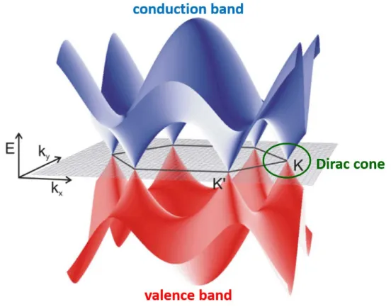
Figure 2.4. Electronic band structure of graphene. The band structure of graphene in the momentum
space is symmetric when 𝑡𝑡′ = 0. The upper 𝜋𝜋 band and lower 𝜋𝜋 band correspond respectively to the conduction and valence bands. In the vicinity of the Dirac points (𝐾𝐾 or 𝐾𝐾′), the energy dispersion is linear and forms a Dirac cone as can be seen in the green circle. Adapted from 4.
Now, we consider the graphene band structure in the vicinity of the 𝐾𝐾 or 𝐾𝐾′ points. To do this, we write 𝑘𝑘�⃗ = 𝐾𝐾��⃗ + 𝑞𝑞⃗. Here, 𝑞𝑞⃗ is the momentum measured relatively to the 𝐾𝐾 or 𝐾𝐾′ points and |𝑞𝑞⃗| ≪ �𝐾𝐾��⃗� . We thus get:
𝐸𝐸±(𝑞𝑞⃗) ≈ ±ћ𝑣𝑣𝐹𝐹|𝑞𝑞⃗| (2.5)
Here, ћ is the reduced Planck constant. This shows that the energy-momentum dispersion given in Eq. 2.4a (for 𝑡𝑡′ = 0) becomes nearly linear and rotationally symmetric close to the 𝐾𝐾 or 𝐾𝐾′ points, yielding a Dirac cone as can be seen in the green circle of Fig. 2.4. Hence,
conduction and valence bands touch or cross at the 𝐾𝐾 or 𝐾𝐾′ points, named as Dirac points. Note that in pristine graphene, the Fermi energy is situated at the Dirac points.
The parameter 𝑣𝑣𝐹𝐹 having a dimension of a velocity is known as Fermi velocity. This physical quantity is directly related to the coupling strength between the adjacent carbon atoms or the nearest-neighbor hopping energy 𝑡𝑡. The expression of 𝑣𝑣𝐹𝐹 is given by:
𝑣𝑣𝐹𝐹 =3𝑡𝑡𝑎𝑎2ћ (2.6)
One can estimate the value of 𝑣𝑣𝐹𝐹 ~ 1 × 10⁶ m/s for 𝑡𝑡 ~ 3 eV. The Fermi velocity is approximately 300 times smaller than the speed of light 𝑐𝑐 ~ 3 × 10⁸ m/s. This shows the
unusual semimetallic behavior of charge carriers in graphene. In other words, they behave as relativistic particles moving with the Fermi velocity 𝑣𝑣𝐹𝐹 and their rest mass is zero. These particles are known as massless Dirac fermions that can be described by a Dirac Hamiltonian. Interestingly, these important results analogous to high-energy physics show that quantum relativistic phenomena can also be investigated and observed in low-energy physics. The particular properties seen in an ideal graphene are therefore an essential starting point to study the electronic properties of carbon-based materials in other dimensionalities.
1.2. Bilayer graphene
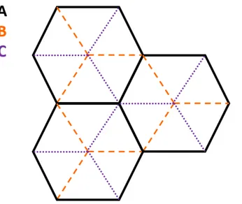
The electronic properties of a single layer of graphene or monolayer graphene have been described in the previous subsection. In reality, a monolayer graphene is very difficult to be isolated experimentally. Naturally, graphene presents in the form of several monolayers stacked in a regular order. Fig. 2.5 clearly shows three possible orientations of graphene layers: A, B and C. The influence of particular stacking orders on the electronic properties of graphene will be discussed later in the text 10,11.
Figure 2.5. Schematic of three different orientations of graphene layers. ABA (Bernal) stacking is
found in bilayer and trilayer graphenes. ABC (rhombohedral)stacking can be found in trilayer graphene. 30