UNIVERSITÉ DE MONTRÉAL
ELECTROLYTE-GATED TUNGSTEN OXIDE TRANSISTORS: FABRICATION, WORKING MECHANISM, DEVICE PERFORMANCE
XIANG MENG
DÉPARTEMENT DE GÉNIE PHYSIQUE ÉCOLE POLYTECHNIQUE DE MONTRÉAL
THÈSE PRÉSENTÉE EN VUE DE L’OBTENTION DU DIPLÔME DE PHILOSOPHIAE DOCTOR
(GÉNIE PHYSIQUE) SEPTEMBRE 2017
ÉCOLE POLYTECHNIQUE DE MONTRÉAL
Cette thèse intitulée :
ELECTROLYTE-GATED TUNGSTEN OXIDE TRANSISTORS: FABRICATION, WORKING MECHANISM, DEVICE PERFORMANCE
présentée par : MENG Xiang
en vue de l’obtention du diplôme de : Philosophiae Doctor a été dûment acceptée par le jury d’examen constitué de :
M. YELON Arthur, Ph. D., président
Mme SANTATO Clara, Doctorat, membre et directrice de recherche M. DESJARDINS Patrick, Ph. D., membre
Mme HEMMER Eva, Dr. Ing., membre
ACKNOWLEDGEMENTS
First and foremost, I would like to express my deepest thanks to my supervisor, Professor Clara Santato, for giving me the opportunity to work in the Advanced Electroactive Materials group, and for her inspiring enthusiasm, scientific guidance, support and encouragement during these last five years. This thesis would never have become reality without her. I also very much appreciate her moral support.
I thank Professor Francesca Soavi for her support and help during my pre-doctoral exam and for working with me on my first paper. I thank Professor Fabio Cicoira for the opportunity to access his lab and for his valuable advice and discussions.
Many thanks to all the colleagues that have contributed to my research projects over the last years. I am very grateful to Patricia Moraille for help in AFM, Dr. Josianne Lefebvre for support during XPS measurements, Christophe Clément for assistance in microfabrication, Dr. Nima Nateghi for assistance in XRD measurements, Dr. Marta Maria Natile for assistance in BET measurements and Dr. Samir Elouatik for assistance in Raman and ATR-FTIR measurements. I also want to thank Yves Drolet, Francis Boutet and Daniel Pilon for their technical assistance in the laboratory. Not less important, I would also like to thank my other colleagues and friends, former and present, Francis, Frederic, Shuang, Hao, Dilek, Jonathan, Julia, Prajwal, Irina, Fanny, Gaia, Guido, Martin, Eduardo, Tian, Xu, Zhaojing and Mengjiao for their support and advice in my research or just interesting discussions outside the laboratory. I will always remember them with their warm hearts and big smiles. Special thanks to Michelle Alexandra Gaspard for proofreading the French abstract. Financial support from the China Scholarship Council is gratefully acknowledged. I am also grateful to CMC Microsystems for the funding provided for microfabrication through programs MNT Financial Assistance and Solutions.
Furthermore, I am grateful to the jury members, Profs. Arthur Yelon, Patrick Desjardins, Kirk Bevan and Eva Hemmer for their time and interest in my work.
Finally, I would like to give a very special thanks to my beloved husband and colleague, Shiming Zhang. We went through all the good and bad moments together in the past 8 years. At last, I would never forget to mention my little one, Mark, who makes my life different!
RÉSUMÉ
Le transistor est l'un des composants clés des ordinateurs, des téléphones cellulaires intelligents, des moniteurs et d'autres produits électroniques qui ont affecté le progrès technologique et scientifique de notre société.
Ces dernières années, l'attention a été consacrée à l'étude des transistors utilisant la commutation électrolytique, au lieu de diélectriques solides conventionnels. Bien que l'utilisation d'électrolytes dans l'électronique ne soit pas un nouveau concept, la commutation électrolytique est importante pour le développement de l’électronique flexible et biocompatible.
Les transistors à commutation électrolytique ont, en effet, attiré l'attention en raison de leur faible tension d'alimentation (< 2 V) ainsi que de la possibilité d'obtenir une densité de charge aussi élevée que 1014-1015 cm-2 en raison de la capacité élevée de l’interface électrolyte/canal du transistor
(1-10 μF·cm-2). Mis à part leur intérêt technologique intrinsèque, les transistors à commutation
électrolytique constituent aussi une plateforme expérimentale pour étudier des aspects fondamentaux. Ils sont en effet utilisés pour étudier le transport combiné électronique et ionique, le transport de charge à haute densité de charge et le contrôle électrique des transitions de phase. Différents électrolytes ont été utilisés comme grille électrolytique, tels que des solutions aqueuses d'électrolyte, des polyélectrolytes, des polymères électrolytiques et des liquides ioniques. Parmi ceux-ci, les liquides ioniques se distinguent par leurs propriétés physico-chimiques uniques. En effet, les liquides ioniques peuvent être conçus pour posséder des caractéristiques de volatilité limitée, bonne conductivité ionique, faible viscosité, stabilité thermique élevée et large fenêtre de stabilité électrochimique (jusqu'à environ 5 V), en sélectionnant la structure appropriée pour le cation et l'anion.
Les oxydes métalliques sont de candidats prometteurs en tant que matériaux de canal pour les transistors à grille électrolytique. Les semi-conducteurs à base d'oxydes de métaux ont été intensément étudiés au cours des dernières décennies pour les transistors, en particulier pour des applications de type affichage, en raison de leur mobilité de charge élevée, de leur transparence optique, de leur stabilité chimique, facilité de mise en forme et faible coût.
Dans cette thèse, nous nous concentrons sur l'oxyde de tungstène qui peut être synthétisé par de simples méthodes en solution, est sensible à la lumière visible et présente de transitions intéressantes isolant-métal (métallisation).
Le noyau de cette thèse est consacré à une meilleure compréhension du mécanisme de fonctionnement des transistors à grille électrolytique à base d’oxydes de métaux, afin d'optimiser leurs performances et de développer de dispositifs optoélectroniques flexibles. Pour étudier le processus de dopage aux interfaces oxyde/électrolyte, une combinaison de voltammétrie cyclique, diffraction aux rayons X et caractérisation de type transistor, complétée par des études spectroscopiques (Raman et infrarouge), a été utilisée. Sur la base de cette étude, un mécanisme de fonctionnement pour les transistors à commutation électrolytique à base d'oxyde de tungstène nanostructuré a été proposé, impliquant le dopage électrostatique, le dopage électrochimique conventionnel et le dopage électrochimique confiné à l'interface.
L'effet de la température du traitement thermique de couches minces semiconductrices d'oxyde de tungstène sur la performance de phototransistors correspondants a été étudié. A cet effet, des couches minces d'oxyde de tungstène traitées thermiquement à 300 °C et 550 °C ont été caractérisées pour leur comportement transistor et phototransistor. En absence de lumière, les transistors à base de couches minces traitées à basse température (300 °C) ont montré des ratios ON/OFF plus élevés que celles traitées à haute température (550 °C). Sous illumination, les couches minces traitées à 550 ºC, sous vide, montrent un phénomène de photoconductivité persistante, limitant ainsi leur intérêt pour des applications de type phototransistor. D'autre part, les couches minces traitées à 300 °C, ne montrent pas de photoconductivité persistante.
Compte tenu des applications optoélectroniques, la principale contribution de cette thèse est le développement de phototransistors flexibles à commutation électrolytique. En particulier, en ce qui concerne les substrats de SiO2, les dispositifs fabriqués sur un polyimide flexible présentent des
performances améliorées en termes de rapport ON/OFF et de photosensibilité. Ces couches minces d’oxyde de tungstène traitées à basse température, caractérisées pour leur performance de type transistor, photosensibilité et photoresponsivité, sont prometteuses pour une nouvelle génération de détecteurs de lumière flexibles de grande surface.
Cette thèse fournit de nouvelles hypothèses sur le mécanisme de fonctionnement des transistors à commutation électrolytique. La thèse démontre aussi la nécessité de considérer les effets de la température du traitement thermique et de la nature du substrat sur la performance de phototransistors. Nos résultats et les techniques que nous avons employées ouvrent la voie à une compréhension globale de la dynamique complexe de dopage à l'interface entre les oxydes métalliques et les électrolytes.
ABSTRACT
Transistors are one of the key components in computers, smart cell phones, monitors and other electronics products, which have affected the technological and scientific progress of our society. In recent years, attention has been dedicated to the study of electrolyte-gated transistors, which utilize electrolytes as the gating layer instead of conventional solid dielectric. Although the use of electrolytes in electronics is not a new concept, new printable, fast-response electrolytes are expanding the potential applications of electrolyte-gated transistors in flexible, rollable and biocompatible electronics.
Electrolyte-gated transistors are indeed attracting attention because of their low driving voltages (< 2 V) as well as the possibility of achieving charge carrier density as high as ca. 1014 −1015 cm−2, owing to the high capacitance of the electrolyte/transistor channel interface (ca. 1−10 μF·cm−2). The intrinsic technological interest of electrolyte-gated transistors is paralleled by their relevance as experimental platforms to study fundamental aspects of electrochemistry, solid state physics and electronic engineering. Particular attention is devoted to combined electronic and ionic transport, charge carrier transport at high charge density and electrical control of phase transitions.
Different electrolytes have been used as gating media in electrolyte-gated transistors, such as aqueous electrolyte solutions, polyelectrolytes, electrolyte polymers and ionic liquids. Among these, ionic liquids stand out due to their unique physicochemical properties. Indeed, ionic liquids can be designed to exhibit limited volatility, good ionic conductivity, low viscosity, high thermal stability, and a wide electrochemical stability window (up to ca. 5 V) by appropriate choice of structure for the cation and anion.
Promising channel material candidates for electrolyte-gated transistors are metal oxides. Metal oxide semiconductors have been intensively investigated over the past decades for transistors, particularly in display applications due to their high charge carrier mobility, high optical transparency, chemical stability, low temperature processability and low cost. In this thesis, we focus on tungsten oxide that features solution processability, insulator-to-metal transition and visible light sensitivity.
The core of this thesis is devoted to a better understanding of the operational mechanism of ionic liquid-gated metal oxide transistors, to optimize their performance and to develop flexible
optoelectronics. To investigate the doping process at oxide/electrolyte interfaces, a combination of cyclic voltammetry, X-ray diffraction, and transistor performance characterizations, complemented by spectroscopic (Raman and infrared) investigations were employed. We correlated the metal oxidation state and the charge transport properties of the metal oxide. Based on this study, a working mechanism for the ionic liquid-gated tungsten oxide was proposed, involving the electrostatic doping as field-effect, conventional electrochemical doping and nonconventional interface-confined electrochemical doping.
The effect of the thermal treatment temperature of the tungsten oxide semiconducting films on corresponding (photo)transistor performance was demonstrated. For this purpose, 550 °C and 300 °C thermally treated tungsten oxide films were characterized for their transistor and photoresponse behavior. In dark condition, low temperature (300 °C) tungsten oxide electrolyte-gated transistors showed higher ON/OFF ratios than high temperature (550 ºC) ones due to the amorphous structure. Under illumination, films treated at 550 ºC, operated in vacuum conditions, show persistent photoconductivity, thus limiting their interest for phototransistor applications. On the other hand, films treated at 300 °C, are persistent photoconductivity-free.
In view of optoelectronics applications, the main contribution of this thesis is the development of flexible electrolyte-gated phototransistors. In particular, with respect to SiO2 substrates, devices fabricated on flexible polyimide show improved performance in terms of ON/OFF ratio and photosensitivity. These low temperature tungsten oxide films, characterized for their transistor, photosensitivity and photoresponsivity behavior, are promising for a new generation of large-area light detectors.
This thesis provides new insights into the working mechanism of electrolyte-gated transistors. It demonstrates the necessity to consider the effects of film thermal treatment temperatures and substrates on the device performance. Our findings and the techniques we employed pave the way for a comprehensive understanding of complex doping dynamics at the interface between metal oxide films and electrolytes and for developing flexible electronics.
TABLE OF CONTENTS
ACKNOWLEDGEMENTS ... III RÉSUMÉ ... V ABSTRACT ...VII TABLE OF CONTENTS ... IX LIST OF TABLES ... XIII LIST OF FIGURES ... XIV LIST OF SYMBOLS AND ABBREVIATIONS... XIX LIST OF APPENDICES ... XXIII
CHAPTER 1 INTRODUCTION ... 1
1.1 Introduction to MOSFET ... 2
1.1.1 Working principle of MOSFET ... 2
1.1.2 Voltage-current characteristics of MOSFET ... 4
1.1.3 Transfer characteristics of MOSFET ... 8
1.1.4 Short channel effect and subthreshold region ... 8
1.1.5 Figures of merit of MOSFET ... 9
1.1.6 Thin film transistors ... 11
1.2 From FET to electrolyte-gated transistors (EGT) ... 12
1.3 Research issue ... 14
1.4 Motivation ... 14
1.5 Objectives ... 15
1.6 Organization of the work ... 16
2.1 Metal oxide semiconductors ... 17
2.2 Tungsten oxide ... 18
2.2.1 Structural, electronic, optical and (electro)chemical properties of WO3 ... 18
2.2.2 Nanostructured WO3 ... 22
2.3 Electrical double layer ... 23
2.3.1 Ionic liquid based EDL ... 24
2.3.2 Capacitance of solid-ionic liquid interfaces ... 25
2.4 Ionic liquid-gated transistors ... 27
2.4.1 Channel materials ... 28
2.4.2 Device architecture ... 35
2.4.3 Working mechanism of ionic liquid-gated metal oxide transistors ... 36
CHAPTER 3 EXPERIMENTAL METHODS AND TECHNIQUES ... 41
3.1 Materials ... 41
3.1.1 WO3 synthesis ... 41
3.1.2 Ionic liquids ... 41
3.1.3 Activated carbon paper ... 42
3.1.4 SiO2/Si and polyimide substrates ... 42
3.2 Microfabrication and substrate cleaning ... 42
3.3 Fabrication: thin film and device ... 43
3.4 Techniques ... 44
3.4.1 Electrochemical characterization ... 44
3.4.2 Transistor characterization ... 46
3.4.3 Structural and compositional characterizations ... 46
3.4.5 Other characterization ... 49
CHAPTER 4 ARTICLE 1: ELECTROLYTE-GATED WO3 TRANSISTORS: ELECTROCHEMISTRY, STRUCTURE, AND DEVICE PERFORMANCE... 51
4.1 Authors ... 51
4.2 Abstract ... 52
4.3 Introduction ... 52
4.4 Experimental Method ... 55
4.4.1 Microfabrication, materials and device assembly ... 55
4.4.2 Characterization ... 55
4.5 Results and Discussion ... 57
4.5.1 Electrochemistry and XRD characterization ... 57
4.5.2 Transistor characterization ... 60
4.5.3 Mechanism of doping ... 63
4.6 Conclusions ... 64
4.7 Acknowledgments ... 64
CHAPTER 5 ARTICLE 2: ELECTROLYTE-GATED PHOTOTRANSISTORS BASED ON TUNGSTEN OXIDE FILMS... 65
5.1 Authors ... 65
5.2 Abstract ... 66
5.3 Introduction ... 66
5.4 Results and Discussion ... 68
5.4.1 Photosensitive electrolyte-gated transistors (EGT) based on polycrystalline tungsten oxide films, operated in ambient conditions and under vacuum ... 68 5.4.2 Electrolyte-gated phototransistors based on tungsten oxide films treated at 300 C . 72
5.4.3 Structural and electrochemical characterization of tungsten oxide films on polyimide
and corresponding ionic-liquid gated phototransistors ... 75
5.5 Conclusions ... 76
5.6 Experimental Section ... 77
5.7 Acknowledgements ... 79
CHAPTER 6 GENERAL DISCUSSION ... 80
CHAPTER 7 CONCLUSION AND RECOMMENDATIONS ... 85
BIBLIOGRAPHY ... 87
LIST OF TABLES
Table 2-1 Specific capacitance calculated from different theoretical models for Pt-ionic liquid interfaces. Capd indicates the capacitance obtained by fitting their EIS data to the RC-RC-model (the electrical double layer at the Pt-ionic liquid interface is considered as a capacitor with a resistive component, in parallel whereas the bulk ionic liquid is considered as a resistor with a capacitive component, in parallel). Cape is the capacitance calculated from impedance analysis according to Z´´= -1/C2πƒA, where ƒ is the frequency of the ac perturbation, A is the electrode area. Maximum capacitance, Capf, is measured with LCR meter using the Cp-mode (resistor and capacitor in parallel) on a Pt/IL/Pt configuration at 20 Hz, dc bias 0 V. (Adapted with permission from Ref. 81, Copyright (2012) American Chemical Society). ... 26 Table 2-2 Capacitance of EDL at 0.1 Hz for the Octathio[8]circulene electrical double layer organic
transistors. (Adapted with permission from Ref. [83]. Copyright (2012) American Chemical Society). ... 27 Table 3-1 Physicochemical properties of the ionic liquids considered in this PhD work.134 ... 42 Table 6-1 Comparison of the device performance of ionic liquid-gated WO3 transistors. ... 82
LIST OF FIGURES
Figure 1-1 Basic structure of a PNP MOSFET showing gate, bulk (n-Si), source (p-doped Si) and drain (p-doped Si) electrodes. The gate is separated from the bulk semiconductor by an oxide layer. ... 2 Figure 1-2 The energy-band diagram of a PNP MOSFET under (a) an applied positive gate bias,
(b) a moderate negative gate bias, and (c) a “large” negative gate bias. ... 3 Figure 1-3 Inversion layer formed (a) at the n-Si/dielectric interface in a PNP MOSFET induced
by applying a large negative bias at the gate; and (b) at the p-Si/dielectric interface in an NPN MOSFET induced by applying a large positive bias. ... 4 Figure 1-4 Ids vs Vds profile in the linear region of the NPN MOSFET represented in the scheme
included in the figure. The black region in the scheme indicates the inversion layer thickness across the channel. ... 5 Figure 1-5 Ids vs Vds profile of the MOSFET represented in the scheme included in the figure,
working at the pinch-off point. The black region in the device scheme indicates the inversion layer thickness across the channel. ... 6 Figure 1-6 Ids vs Vds profile of the MOSFET represented in the scheme included in the figure,
working in the saturation region. The black region of the scheme indicates the inversion layer thickness across the channel. ΔL indicates the length of the pinch-off extension. ... 7 Figure 1-7 Ids vs Vds profile of the MOSFET represented in the scheme included in the figure,
working in the breakdown region. ... 8 Figure 1-8 Illustration of a typical transfer curve (Ids vs Vgs) of a MOSFET. ... 8 Figure 1-9 TFT structures: a) top gate, top source-drain contact; b) top gate, bottom source-drain
contact; c) bottom gate, top source-drain contact; and d) bottom gate, bottom source-drain contact. ... 12 Figure 1-10 Working mechanism of an electrolyte-gated n-type transistor based on (a) electrostatic
Figure 2-1 Schematic of (a) bandgap formation mechanism and (b) carrier transport paths for covalent (silicon) and ionic oxide semiconductors. (Reprinted with permission from Ref. 42, Copyright © 2010, Nature Publishing Group) ... 18 Figure 2-2 Structural models for tungsten oxide: (a) low temperature monoclinic, triclinic; (b) room
temperature monoclinic; (c) orthorhombic; (d) tetragonal and (e) simple cubic. (Reprinted with permission from Ref. 52, Copyright 2000, International Union of Crystallography) .... 19 Figure 2-3 DOS of cubic WO3. When energy is below 0 eV, filled states are found; empty states
are found when energy is above 0 eV. (Reprinted with permission from Ref. 53, Copyright © 1996, American Physical Society) ... 20 Figure 2-4 Transmission spectra of radio-frequency (RF) magnetron sputtered WO3 films on
optical grade quartz substrates with different substrate temperatures (Reprinted with permission from Ref. 59, Copyright 2010, AIP Publishing LLC) ... 21 Figure 2-5 Scheme of the (a) Helmholtz, (b) Gouy-Chapman and (c) Gouy-Chapman-Stern Models
for the electrical double layer at an electrolyte/electrode interface. ... 23 Figure 2-6 (a) Scheme of the multilayer model for electrical double layers at ionic liquid/ electrode
interface. (b) Potential changes in an electrode/ionic liquid/semiconductor configuration. .. 25 Figure 2-7 Cross section of a rubrene ionic liquid-gated transistor. (Reprinted with permission from
Ref. 102, Copyright (2011) American Chemical Society). ... 29 Figure 2-8 (a) Molecular structures of the ionic liquid, [DEME][TFSI] (top) and the cross-section
of ionic liquid-gated ZnO transistors (bottom). (b) Sheet carrier density and Hall mobility as a function of gate voltage at 300 K, determined by Hall effect measurements. (Reprinted with permission from Ref. 92. Copyright 2009 WILEY ‐VCH Verlag GmbH & Co. KGaA, Weinheim) ... 31 Figure 2-9 (a) Schematic and optical image of an ion-gel-([EMI][TFSI]+PS-PMMA-PS)-gated
solution processed In2O3 transistor. (b) Electron density from Hall effect (nHall), and from displacement current (nFET) versus Vg. (c) Hall mobility (μHall) versus Vg; nHall is labeled in correspondence of each point. (Reprinted with permission from Ref. 116, Copyright 2017 WILEY‐VCH Verlag GmbH & Co. KGaA, Weinheim.) ... 32
Figure 2-10 (a) Temperature dependence of the sheet resistance (Rs) for VO2 film with different gate voltages (Vg). (b) Temperature dependence of Rs for VO2 film with different thickness, 10-, 20- and 70-nm, showing both initial (Vg = 0 V) and electric-field-induced metallic states. (Reprinted with permission from Ref. 118, Copyright 2012 Nature Publishing Group.) ... 33 Figure 2-11 (a) Schematic of charge accumulation by an electric double layer formed at an interface
between [DMIM][TFSI] and ZrNCl. (Reprinted with permission from Ref. 122, Copyright 2009 Nature Publishing Group.) ... 34 Figure 2-12 (a) Schematics of the VO2 EGT devices with planar (top) and vertical (bottom) gate
geometry. (b) Parameters (top) (gate geometry, channel dimension, and the ionic liquid material) for different VO2 EGT devices and their performance (bottom) at 25 °C. (Reprinted with permission from Ref. 123, Copyright 2012 AIP Publishing LLC.) ... 35 Figure 2-13 The θ-f plots in (a) Pt/ionic liquid/Pt and (b) Pt/ionic liquid/ZnO structures at varied
biases. Inset: equivalent electric circuit and cross section of positively biased ZnO electrical double layer transistor. (c) Charge carrier densities as a function of Vg from Hall measurement (red dots) and from the C-Vg integration (blue dots for 1 Hz and green dots for 0.1 Hz). (d) Temperature-frequency mapping for the phase angle of the Bode plot. (Reprinted with permission from Ref. 124, Copyright (2010) American Chemical Society.) ... 37 Figure 2-14 Scheme of the Hall bar device geometry to test for long-range effects in oxide thin
films away from the area being charged. The spacing of voltage contacts was 300 μ m for all devices. (Reprinted with permission from Ref. 125, Copyright © 2016, X. Leng, A. T. Bollinger and I. Božović) ... 38 Figure 2-15 Suppression of the metal-insulator temperature in VO2 films. (a) Sheet resistance vs
temperature for various gate voltages for VO2/TiO2 (001). (b) Resistivity of VO2 vs temperature as a function of oxygen pressure during film deposition. (c) Sheet resistance of VO2 electrolyte-gated devices on TiO2 (001) and Al2O3 (1010) and electron carrier density ne from Hall measurements for an electrolyte-gated device fabricated from VO2/TiO2 (001), vs Vg. The dashed line is a guide to the eye. (d) Source-drain current (device fabricated from VO2/Al2O3 (1010)) vs time as oxygen pressure was varied from 150 torr to 10−5 torr to 130 torr and to 10−5 torr at Vg = 3 V. (Reprinted with permission from Ref. 37, Copyright © 2013, American Association for the Advancement of Science.) ... 40
Figure 3-1 Device structure of electrolyte-gated WO3 transistor fabricated on a SiO2 substrate with patterned Au source and drain electrodes. A Pt wire was used as a probe to contact the gate electrode. ... 44 Figure 3-2 Cyclic voltammetry three electrode system cell (a), potential—time profile to perform
cyclic voltammetry (b), (c) Cyclic voltammogram depicting the peak positions, EP, and peak height, IP.137 ... 45 Figure 4-1 Schematic of the ionic liquid-gated WO3 EG transistor studied in this work. Durapore®
GVHP membrane filter soaked with the ionic liquid was put on top of the transistor channel, carbon paper coated with high surface area carbon ink was set in contact with the membrane and used as the gate electrode. Molecular structures of the ionic liquids [EMIM][TFSI] and [PYR14][TFSI] were used to gate the transistors. ... 56 Figure 4-2 Cyclic voltammetry of the WO3 channel in transistor configuration with [EMIM][TFSI]
(a) or [PYR14][TFSI] (b) as the electrolyte, at various scan rates (10, 50, and 100 mV/s). XRD patterns in the 20°-60° (c) and in the zoomed 25°-60° region (d) obtained from: as-prepared WO3 films -on-ITO (A), WO3 films-on-ITO electrodes biased for 5 min at -0.6 V (B) and -1 V (C), in [EMIM][TFSI]. ... 58 Figure 4-3 Transfer characteristics of (a) [EMIM][TFSI]-gated and (b) [PYR14][TFSI]-gated WO3
transistors in the saturation regime (Vds = 1 V). Ids (left axis, black solid line) and Igs (gate-source current, right axis, gray dotted line) plotted vs. Vg, scan rate is 10 mV·s-1. Inset: output characteristics, Vg = 0 V to 0.8 V in steps of 0.2 V, Vds scan rate is 10 mV·s-1. ... 61 Figure 5-1 [EMIM][TFSI]-gated photosensitive transistors based on tungsten oxide films (483 ± 47
nm-thick) treated at 550 °C on SiO2 substrates, characterized in ambient conditions. (a) Transfer characteristics in the linear regime (Vds = 0.2 V), Vg scan rate 10 mV·s−1, in the dark (black) and under illumination (red). (b) Output characteristics in the dark and under illumination, Vg = 0, 0.4, 0.6, 0.8 V, Vds scan rate 10 mV·s−1. (c) Transient (Ids - time) measurements under chopped light (light on, light off indicated by red line) at Vds = 0.2 V, Vg = 0.1 V. ... 69 Figure 5-2 [EMIM][TFSI]-gated photosensitive transistors based on tungsten oxide films (483 ± 47
nm-thick) treated at 550 °C on SiO2 substrates characterized in vacuum. (a) Transfer characteristics in the linear regime (Vds = 0.2 V), Vg scan rate 10 mV·s−1, in the dark (black)
and under illumination (red). (b) Output characteristics in dark and under illumination, Vg = 0, 0.6, 0.8, 1.0, 1.2 V, Vds scan rate 10 mV·s−1. (c) Ids-time measurements under chopped light (indicated by red line) at Vds = 0.2 V, Vg = 0.1 V. ... 70 Figure 5-3 [EMIM][TFSI]-gated phototransistors based on tungsten oxide films (120 ± 26 nm-thick) treated at 300 °C on SiO2 substrates, characterized in vacuum. (a) Ids-time measurements under chopped light (indicated by red line), at Vds = 0.2 V, Vg=0.1 V. (b) Transfer characteristics in the linear regime (Vds = 0.2 V), Vg scan rate 10 mV·s−1; dark (black) and illumination (red) conditions. (c) Output characteristics under dark and illumination conditions, Vg=0, 0.6, 0.8, 1.0, 1.2 V, Vds scan rate 10 mV·s−1. (d) Responsivity and sensitivity vs Vg recorded at Vds = 0.2 V; lines are guides for the eye. ... 73 Figure 5-4 [EMIM][TFSI]-gated phototransistors based on tungsten oxide films (153 ± 25 nm-thick) treated at 300 °C on polyimide substrates, characterized in vacuum. (a) Au-patterned PI substrates. (b) Responsivity and sensitivity vs Vg recorded at Vds = 0.2 V. Lines are guides for the eye. ... 75
LIST OF SYMBOLS AND ABBREVIATIONS
Beti Bis(pentafluoroethylsulfonyl)imideBMIM 1-butyl-3- methylimidazolium BMMIM 1-buyl-2,3-dimethylimidazolium
c Light speed
CBM Conduction band minimum C0 Specific capacitance
CMOS Complementary metal–oxide–semiconductor CPU Central processing unit
c-Si Crystalline silicon CV Cyclic voltammetry d Dielectric thickness
De- Electrondiffusion coefficient
DEME N, N-diethyl-N-(2-methoxyethyl)-N-methylammonium DM+ Ion (M+) diffusion coefficient
DOS Density of state
e Elementary charge
E Electric field
EC Conduction band energy ECT Electrochemical transistor EDL Electrical double layer
EDLT Electrical double layer transistor
EF Fermi level
Eg Bandgap
EG Electrolyte-gated
EMI 1-ethyl-3-methyl imidazolium EMIM 1-ethyl-3-methylimidazolium EMMIM 1-ethyl-2,3-dimethylimidazolium
EV Valance band energy
ƒ Frequency of the ac perturbation FAP Tris(perfluoroethyl)trifluorophosphate FET Field-effect transistors
gm Transconductance h Planck constant H Hydrogen HMIM 1-hexyl-3-methylimidazolium HMDS Hexamethyldisilazane Ids Source-drain current
Idsat Saturation source-drain current
IL Ionic liquid
Im bis(triflouromethylsulfonyl)amide Ioff Off state current
Ion On state current ITO Indium tin oxide
JFET Junction field effect transistors
L Channel length
MO Metal oxide
MOSFET Metal–oxide–semiconductor field-effect transistor NMP N-methyl pyrrolidone
NPN p-Si bulk, n-doped Si electrodes OTf Trifluoromethanesulfonate
p Charge carrier density
P13 N-methyl-N-propyl-pyrrolidinium P14 1-butyl-1-methylpyrrolidium P3HT Poly(3-hexylthiophene-2,5-diyl) PEG Poly (ethylene glycol)
PEN Polyethylene naphthalate PF6 Hexafluorophosphate
PNP n-Si bulk, p-doped Si electrodes PQT-12 Poly (3,3‴-didodecylquaterthiophene PVDF Polyvinylidene fluoride Q Doping charge RC Resistor-capacitor S Subthreshold swing TCB Tetracyanoborate TFSI Bis(trifluoromethylsulfonyl)imide TFT Thin film transistor
TMI Metal-insulator transition temperature
VBM Valence band maximum
Vgs Gate-source voltage Vth Threshold voltage W Channel width α Absorption coefficient µn Electron mobility ν Photon frequency
ʋn Electron drift velocity ɛ0 Vacuum permittivity
ɛ Relative permittivity of dielectric
LIST OF APPENDICES
APPENDIX A – SUPPORTING INFORMATION FOR ARTICLE 1 ... 98 APPENDIX B – SUPPORTING INFORMATION FOR ARTICLE 2 ... 110 APPENDIX C– LIST OF PUBLICATIONS IN POLYTECHNIQUE MONTREAL NOT
INCLUDED IN THE THESIS ... 121 APPENDIX D – PARTICIPATION AT CONFERENCES ... 122
CHAPTER 1
INTRODUCTION
In this chapter, we give a brief overview of transistor technology as well as the structure and the working principle of metal oxide semiconductor field-effect transistors, MOSFET, to provide the background needed to understand the scientific and technological findings of this PhD thesis. Electrolyte gating principles are also discussed. Research issues, motivation, main objective, specific objectives and organization of the work are included.
History of transistors
Two revolutionary historic events changed the communication between human beings. The first one, the “Age of Discovery,” started in the early 15th century and continued to the 17th century. During this period, Europeans explored Africa, America, Asia and Oceania, connecting humans geographically. The second one is the development of the “Internet” in the early 1960s, which rapidly spread to the whole world, and connected and synchronized our thinking.1 Mobile electronic devices are the carriers of the Internet and the “brain” of mobile devices is the central processing unit (CPU). The CPU contains billions of tiny field-effect transistors (FET) to manipulate the flow of electrons in semiconductors, to allow the processing or storage of information. In 1926, the first FET was patented by Lilienfeld but FET failed to achieve fame at that time because of the poor quality of semiconductor materials.2 In 1950, the more practical junction FET (JFET) was invented by the Japanese engineers Nishizawa and Watanabe.3 In 1952, the researchers Bardeen, Brattain, and Shockley of Bell Labs independently invented the JFET.4 In particular, Shockley’s attempt to commercialize the FET in the 1950s led to California's "Silicon Valley" that became a hotbed of electronics innovation. Finally, in 1956, these three scientists were jointly awarded the Nobel Prize in Physics for “their researches on semiconductors and their discovery of the transistor effect.”5 In 1959, Kahng and Atalla at Bell Labs invented the MOSFET.6 Since then, MOSFET has become the most common transistor used in digital circuits. Two complementary configurations of MOSFET, the n-channel MOSFET and the p-channel MOSFET, were then fabricated.7 Electronic circuit design becomes very versatile when these two types of devices are used in the same circuit. These circuits are referred to as complementary MOS (CMOS) circuits. Millions of CMOS FET integrated together build the basic units of a memory chip, microprocessor and CPU, which are the fundamental units of the electronics we are using now, such as cameras, smart phones and the computers.
Transistors, featuring different structures, are presently experiencing an explosive evolution towards lightweight, flexible, stretchable and biocompatible electronics, e.g. for next-generationwearable and textile integrated systems,8-10 flexible and rollable displays,11, 12 medical implants13 and artificial skin.14, 15
1.1 Introduction to MOSFET
1.1.1 Working principle of MOSFET
Here we will discuss the working principle of the MOSFET, which is important to understand the content of this thesis. The core of a MOSFET is analogous to a capacitor where one plate is the gate electrode and the other plate is the semiconductor (Figure 1-1). A dielectric layer is sandwiched between these two plates. For a PNP MOSFET, when we apply a negative electrical bias to the gate, positive charge accumulates on the semiconductor side. In the case of the N-silicon channel shown in Figure 1.1, this happens via hole transport from the bulk of the semiconductor to the interface with the dielectric.
Figure 1-1 Basic structure of a PNP MOSFET showing gate, bulk (n-Si), source (p-doped Si) and drain (p-doped Si) electrodes. The gate is separated from the bulk semiconductor by an oxide layer.
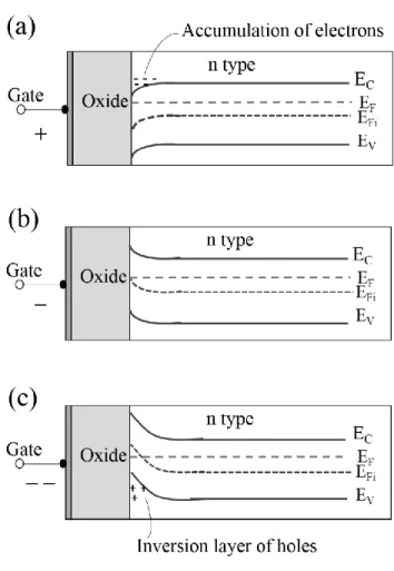
The hole accumulation at the dielectric/semiconductor interface can be related to the energy level bending, as shown in Figure 1-2. For n-Si, upon application of a positive bias at the gate, the conduction band (EC), valence band (EV), and the intrinsic Fermi energy (EFi) levels all “bend down” (Figure 1-2a). Therefore, Ec is closer to the Fermi level (EF), indicating a higher electron density at the interface with the dielectric. Analogously, when we apply a negative bias, a corresponding positive net charge will be induced at the n-silicon/dielectric interface. The positive
charge “bends up” the energy levels so that EV is closer to EF, indicating a higher hole density in the channel (Figure 1-2b).
Figure 1-2 The energy-band diagram of a PNP MOSFET under (a) an applied positive gate bias, (b) a moderate negative gate bias, and (c) a “large” negative gate bias.
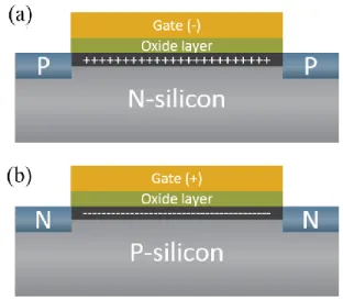
When we continue to increase the negative bias, the bands will bend up more strongly. When a sufficiently large bias is applied, the EFi can bend above EF. This is of great importance since it means the holes became the majority charge carrier at the interface. In this case, the conduction type in n-Si at the interface with the insulator has been inverted from n- to p-type (Figure 1.2c). This p-type surface layer is induced not by chemical doping but simply by applying an electrical bias to the gate (electrostatic doping). An analogous mechanism is applicable to NPN MOSFET in which the conduction type in the p-Si can be inverted from p- to n-type. The inversion layer is the
key to MOSFET operation because it creates a connection between source and drain electrodes, creating current flow between them (Figure 1-3).
Figure 1-3 Inversion layer formed (a) at the n-Si/dielectric interface in a PNP MOSFET induced by applying a large negative bias at the gate; and (b) at the p-Si/dielectric interface in an NPN MOSFET induced by applying a large positive bias.
1.1.2 Voltage-current characteristics of MOSFET
For an NPN MOSFET, the n-type source and drain regions are diffused into a lightly doped p-type substrate and an oxide layer separates the gate electrode from the semiconductor. No significant current flows from source to drain without applying gate voltage (Vgs). When a positive Vgs is applied, the electron concentration increases in the channel. If we further increase Vgs, an inversion layer forms and the channel changes to n-type. The minimum Vgs required to invert the semiconductor from p-type to n-type is called threshold voltage (Vth). When Vgs =Vth, a current flow occurs from the source to the drain. However, actually, Vgs should be larger than Vth because of the presence of the source-drain voltage, Vds.
In the following, we will discuss in detail the operation of an NPN MOSFET. An analogous behavior, taking into account the opposite polarities, is observed with PNP MOSFET.
i) Cut-off region of the transistor (Vgs<Vth)
In the cut-off region, as Vgs<Vth, the electron density increases because of the action of Vgs, but the surface of the semiconductor is either still p-type or a depletion layer is formed. In this mode, there
is negligible current flow from source to drain. However, when we shrink the device dimension (the channel length), the diffusion and drift of the electrons from the source electrode will result in a significant increase of the transistor current even when Vgs < Vth. In this case, the device works in the subthreshold region (details will be discussed later).
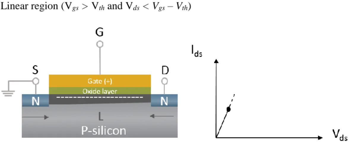
ii) Linear region (Vgs > Vth and Vds < Vgs – Vth)
Figure 1-4 Ids vs Vds profile in the linear region of the NPN MOSFET represented in the scheme included in the figure. The black region in the scheme indicates the inversion layer thickness across the channel.
When we increase Vgs, an inversion layer forms at the interface and an n-type conducting channel is induced. Electrons are able to flow from the source to the drain upon application of a small Vds. In this case, the channel behaves like a resistor. Ids increases linearly with Vds (Figure 1-4). The Ids profile can be described by equation (1):
(1)
Where C0 = ɛ0ɛ/d is the dielectric specific capacitance, ɛ0 is the permittivity of the vacuum and has the value of 8.85 × 10⁻¹² F·m−1, ɛ is the relative permittivity for a given gate dielectric material, d is the thickness of the dielectric, µn is the electron mobility, W is the channel width and L is the channel length.
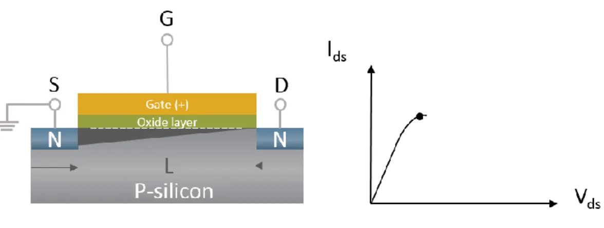
iii) Channel pinch-off (Vds =Vgs –Vth)
gs th
ds n ds V V V L W C I 0 Figure 1-5 Ids vs Vds profile of the MOSFET represented in the scheme included in the figure, working at the pinch-off point. The black region in the device scheme indicates the inversion layer thickness across the channel.
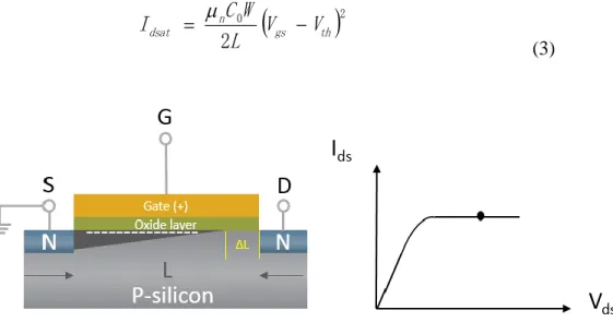
Pinch-off is a key phenomenon in MOSFET. The effective voltage drop at the semiconductor/insulator interface is Vgs –Vds. When Vds is small, Vgs –Vth >> Vds, device works in the linear region. However, when we further increase Vds until Vgs –Vth = Vds, the inversion layer thickness at the drain electrode will become zero. This is the channel pinch-off (Figure 1-5). The minimum Vds required for the channel pinch-off is named Vd sat, and the corresponding Ids is named Id sat.
iv) Saturation region (Vgs –Vth < Vds)
When Vds further increases and Vds > Vgs –Vth, the pinch-off point moves towards the source electrode (Figure 1-6). The additional voltage Vds –Vd sat drops only on the pinch-off region (space charge region). The extension of the pinch-off region increases with increasing Vds, but because the space charge region has much higher resistance compared to the inversion layer and much smaller length (ΔL) compared to the total channel length (L), the electrical field E = (Vds –Vd sat)/ΔL is very strong. In this case, electrons flow in the channel from the source through the inversed channel toward the drain; they are then injected into the pinch-off area, where they are quickly swept by the strong E (even though the region is non-conductive) to the drain electrode. When we further increase Vds, Ids will saturate since the additional voltage applied (Vds –Vd sat) will be absorbed by the pinch-off area (ΔL). For Vds > Vd sat, the current does not change and Vd sat can be described as follows:
(2)
Considering the channel length L –ΔL ≈ L, the current-voltage profiles in equation (1) can be described by:
(3)
Figure 1-6 Ids vs Vds profile of the MOSFET represented in the scheme included in the figure, working in the saturation region. The black region of the scheme indicates the inversion layer thickness across the channel. ΔL indicates the length of the pinch-off extension.
v) Breakdown region
When Vds reaches higher values than the reverse breakdown voltage for the PN junction at the drain region, the saturation current sharply increases and MOSFET starts to work in the breakdown region (Figure 1-7). This situation should be prevented since in most cases, the voltage-current characteristics are non-reversible and may destroy the MOSFET.
th gs dsat
V
V
V
2 0 2 gs th n dsatV
V
L
W
C
I
Figure 1-7 Ids vs Vds profile of the MOSFET represented in the scheme included in the figure, working in the breakdown region.
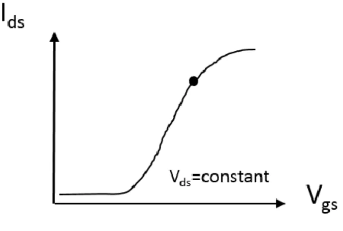
1.1.3 Transfer characteristics of MOSFET
The transfer characteristics relate Ids to the input Vgs, at constant Vds. When Vgs < Vth, the device works in the cut-off region, so the transistor current is negligible. When Vgs > Vth, Ids increases with increasing Vgs due to the channel inversion (Figure 1-8).
Figure 1-8 Illustration of a typical transfer curve (Ids vs Vgs) of a MOSFET.
1.1.4 Short channel effect and subthreshold region
The assumption, L –ΔL ≈ L, for devices working in the saturation region is a good approximation only for long channel MOSFET. However, when the device dimension shrinks (e.g. the Intel 22 nm technology)16 the channel length becomes very small. As a result, the ratio ΔL/L dramatically
increases and causes a considerable decrease in the effective channel length. This is the channel length modulation effect. In this case, the effective channel length L – ΔL decreases with increasing Vds and consequently results in a resistance decrease. Thus, following equation (1), Ids increases with Vds and does not show saturation as Vds increases. This is the short-channel effect. In the cut-off region, we discussed that the Ids is negligible. This is a good approximation for long-channel devices. Taking the example of an NPN MOSFET, when the channel length decreases, the electrons from the source region can diffuse into the weak inversion layer (Vgs < Vth). In the weak inversion layer, the hole concentration decreases, so the electrons can travel through the P channel and can be collected by the drain region. As a result, a short channel device works even in the cut-off region (Vgs < Vth), i.e. there is Ids flow in the device. Short-channel devices working in this mode are called to work in subthreshold mode.
1.1.5 Figures of merit of MOSFET
ON/OFF ratio: In a MOSFET, the saturation current (Idsat) is referred to as the on-state current, Ion. The leakage current (cut-off region) is referred to as off-state current, Ioff. Ion/Ioff is the ON/OFF ratio. A high Ion/Ioff indicates good switching properties, which is required for digital circuits application. In particular, a low Ioff is needed in real devices. A small leakage current through the channel means that the device consumes less electricity, i.e. it requires a low standby power. Transconductance: It is the change in Ids with respect to the corresponding change in Vgs, expressed as follows:
(4)
It indicates the Ids sensitivity to Vgs; it is an important parameter, e.g. for sensor applications of transistors. Following equation (1), the gm in the linear region is obtained:
(5) Following equation (3), the gm in the saturation region is obtained:
const m Vds gs ds V I g const m ds V gs ds V I g ds n V L W C0
(6)
Mobility: In a semiconductor, the electron drift velocity (ʋn) is proportional to the applied electric field (E).
(7)
The proportionality factor (μn) is the electron mobility, with units of cm2 V-1 s-1. A high mobility is attractive for high frequency electronic devices.
The Vth and the mobility μn of semiconductor in a MOSFET can be calculated by linear fitting the equation (5). In the saturation region, both Vth and μn can be obtained by fitting the Ids1/2 versus Vgs using equation (3) as:
(8)
The slope permits us to extract μn and the intercept of Ids at the Vgs axis permits us to extract Vth. μn is usuallydifferent from theintrinsic mobility of bulk material. This is because charge transport in MOSFET occurs in a narrow channel region close to the gate dielectric/semiconductor interface, where different sources of scattering are happening, such as Coulomb scattering from dielectric charges, surface roughness scattering and others.17
Subthreshold swing: As previously discussed, for a MOSFET, when there is a small increment in Vgs, a weak inversion layer changes to strong inversion layer and the device starts to work in the linear region. The subthreshold swing, which reflects the change of Vgs required to increase Ids by an order of magnitude in the subthreshold region, is described by the following equation:
(9)
A small subthreshold swing demonstrates a fast transition between the ON state and OFF state of a MOSFET, thus it is an important parameter in digital circuits or electrical switches that use ON (0) and OFF (1) as the fundamental units.
gs th
n V gs ds m V V L W C V I g ds 0 constE
v
n
n
gs th
n at V V L W C I 2 0 ds
ds
gs I d dV S log For more details of MOSFET model establishment, theory, equation derivation, one can refer to classic books on semiconductor physics and devices.18-20
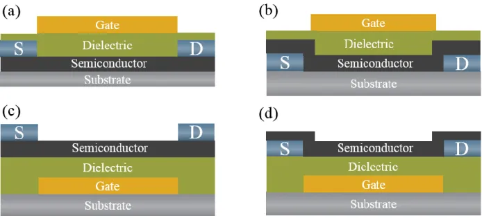
1.1.6 Thin film transistors
The thin film transistor (TFT) is a special kind of field-effect transistor where the semiconductor is deposited as a thin film on an insulating substrate, such as glass or plastic. The first thin film FET was developed at RCA laboratories by Weimer in 1961 with polycrystalline cadmium sulphide (CdS) as the semiconducting thin film and silicon monoxide (SiO) as the dielectric.21 Semiconductors used in TFT are commonly amorphous silicon and polysilicon.22 Cadmium selenide,23 metal oxides17, 24, 25 and organic materials26, 27 have also been widely used. The working principle of TFT refers to that of a MOSFET. One of the differences between the two types of transistors is that the source and drain regions are made of metal electrodes (rather than heavily doped p(n)-type regions in the n(p)-type substrate) so that the p(n)-type inversion layer is not needed to connect the p(n)-type source and drain regions. In this Ph. D. thesis, we will study metal oxide TFT, working in n-type accumulation mode.
Figure 1-9 shows four common device configurations used for TFT. The figure includes: (a) top gate (gate deposited on top of the dielectric), top source-drain contact (the contacts are deposited atop the semiconductor); (b) top gate, bottom contact (the contacts are deposited under the semiconductor); (c) bottom gate (dielectric deposited on top of the gate), top source-drain contact and (d) bottom gate, bottom source-drain contact. Selecting a proper device configuration is important since the configuration can affect the morphology of the channel material, the charge carrier mobility and other device characteristics.
Figure 1-9 TFT structures: a) top gate, top source-drain contact; b) top gate, bottom source-drain contact; c) bottom gate, top source-drain contact; and d) bottom gate, bottom source-drain contact.
1.2
From FET to electrolyte-gated transistors (EGT)
Using transistors for applications such as in vivo,28, 29 wearable30, 31 and low power consumption requires transistors operating at low voltage.32 To decrease the operation voltage, a high capacitance gate dielectric layer is needed. Towards this goal, many different strategies can be used, such as reducing the thickness of the gate dielectric and employing a high permittivity (κ) gate dielectric material.33 The former strategy is often accompanied by a high leakage current; a decreased charge carrier mobility has been frequently reported for the latter,34 due to additional energetic disorder that enhances charge carrier localization.
An interesting way to achieve high capacitance is electrolyte-gating, i.e. the use of electrolytes and ion including media (e.g. ionic liquids) as the gating medium. The key concept behind electrolyte-gating is the electric double layer (see Section 2.3). The capacitance of electrical double layers is typically on the order of 10 µF/cm2, which makes it possible to operate electrolyte-gated transistor (EGT) at relatively low gate voltages (< 2 V) achieving large charge carrier densities (~1015 cm-2) in the channel. This high charge carrier density explains the significant impact of EGT in solid-state physics; EGT enable novel functions and properties, which are extremely difficult or even impossible in conventional all-solid electronic devices (see section 2.4).
As in conventional FET, the gating dielectric, electronically insulating yet ionically conductive, is used to bridge the gap between the metal gate electrode and the channel. The redistribution of the ions at the electrode/electrolyte and electrolyte/channel interfaces upon application of gate voltage results in accumulation (depletion) of charge carriers in the channel. In terms of operating mechanism, EGT can be divided, at least, into two kinds of transistors, i.e. electrical double layer transistors (EDLT) and electrochemical transistors (ECT).35 In case of EDLT, the semiconductor channel is impermeable to the ions of the electrolyte. Therefore, the application of an electrical bias to the gate electrode will cause migration of ions at the electrolyte/gate and electrolyte/semiconductor interfaces, paralleled by accumulation/depletion of charge carriers in the transistor channel, at the interface with the electrolyte (Figure 1-10a).36 The resulting doping is electrostatic. In ECT, the semiconductor channel material allows the ions to enter the film (Figure1-10b). A reversible electrochemical doping (dedoping) process takes place. The doping/dedoping process is responsible for the conductivity change of the channel. Beside these two mechanisms, in 2013, Parkin et al. reported a different operating mechanism for metal oxide EGT. They found that the strong electric field between the ionic liquid gating medium 1-hexyl-3-methylimidazolium bis(trifluoromethylsulfonyl)-imide (HMIM-TFSI) and the VO2 channel material induces oxygen vacancies in the VO2 channel.37 These results demonstrate that EGT permit the study of electronic phase transitions of metal oxide semiconductors.
Figure 1-10 Working mechanism of an electrolyte-gated n-type transistor based on (a) electrostatic and (b) electrochemical doping mechanism.
1.3 Research issue
Despite the growing interest in EDLT and ECT, the physicochemical processes determining the device characteristics are still not well understood.
In particular, the nature of the electrical double layer at the interface between ionic media and porous semiconductors, e.g. nanostructured metal oxides, is still largely undiscovered. This type of interface is much more complex than a geometrically well-defined interface because the electrolyte can penetrate into the porous semiconductor. A slightly different doping mechanism can be hypothesized for these materials, in addition to electrostatic and conventional electrochemical doping, i.e. electrochemical doping confined at the electrolyte/metal oxide interface, especially for electrolytes made up of ions with relatively large size (e.g. ionic liquids), which may not be able to be inserted in the oxide lattice. Therefore, an in-depth study of the working mechanism of EGT based on nanostructured metal oxide channels and ionic liquid gating media could help to advance the knowledge of the doping mechanism at the fundamental level. From an application point of view, while EGT offer great potential for flexible electronics, fabrication of high performance transistors with low processing temperature (e.g. 150 ºC in the case of polyethylene naphthalate (PEN) and 350 ºC for polyimide) is still a challenge. In addition, even though EGT have been used in logic circuits and memory devices, little is known about their application in optoelectronics, e.g. light-emitting transistors and phototransistors.
1.4 Motivation
Among metal oxide semiconductors, tungsten oxide is a promising material for applications such as electrochromic displays,38, 39 gas sensors40 and photodetectors41. Electrolyte gating is attracting growing interest for low operating voltage < 2 V transistors and high charge carrier density (up to 1015/cm2) possibly leading to the discovery of novel electronic phases. Furthermore, electrolyte gating ideally suits possible flexible electronics developments. Fabricating electrolyte-gated transistors based on solution-processed nanostructured tungsten oxide thin films and shedding light on the transistor working principle will permit us to better assess their potential in the field of printable, flexible electronics and, considering the optical absorption properties of tungsten oxide, optoelectronics (e.g. phototransistors).
1.5 Objectives
The main objective of this thesis is to design, fabricate and characterize tungsten oxide transistors using the electrolyte gating approach, for flexible electronics applications.
Solution-processed tungsten oxide thin films with mesoporous nanostructure and high surface area are expected to have a peculiar doping mechanism, different from the mechanism proposed for its single crystal and nonporous film counterparts. Therefore, the first specific objective of this PhD thesis is:
1) Study the electrolyte gating process in transistors based on tungsten trioxide films with mesoporous nanostructure interfaced to ionic liquids to shed light on the doping mechanism. The objective has been accomplished by extended cyclic voltammetry (CV), X-ray diffraction (XRD) and device characterization of EG transistors. The results enrich the current understanding of electron/ionic electroactivity at metal oxide/electrolyte interfaces.
Since the performance of transistors strongly depends on the morphology and structure of the channel materials, the second specific objective is:
2) Investigate the effect of the temperature of thermal treatment of the films and nature of the film substrate (conventional SiO2 vs plastic) in establishing the transistor characteristics, to explore possible flexible developments of the devices.
The use of substrates different from conventional thermal silicon dioxide or glass, e.g. plastics, requires the use of low temperatures of thermal treatment. This temperature affects the morphology and structure of the channel, in turn affecting the doping process. Scanning Electron Microscopy, Atomic Force Microscopy, electrochemical and device characterization of novel electrolyte-gated transistors on polyimide were conducted.
Electrolyte-gated transistors based on photosensitive semiconductors can be interesting from the photodetection point of view because the high density of accumulated charge carriers can improve their photoresponsivity. The third specific objective is therefore the following:
3) Fabricate phototransistors in electrolyte gating configuration, exploiting the multifunctionality of metal oxides.
The combined electrical and photo response of tungsten oxide thin films in EGT configuration were investigated; the results permit to shed light on the working principle of electrolyte-gated phototransistors, in particular the photoresponsivity when the transistor is ON. In turn, the dual optical/electrical effect of such transparent transistors (90% transmittance at 600 nm of the semiconducting tungsten oxide films) can be relevant for numerous applications, such as touch screen, optical switch and photodetecting devices.
1.6 Organization of the work
An introduction to metal oxides and detailed physical and chemical properties of WO3 are contained in Chapter 2. In this same chapter, we include a literature review about electrolyte-gated metal oxide transistors (channel materials, device structures, working mechanisms). Chapter 3 is the experimental part, where materials and techniques used in this thesis are described. Chapter 4, which addresses the first objective of this PhD thesis, is the reproduction of article “Electrolyte-Gated WO3 Transistors: Electrochemistry, Structure, and Device Performance” published in the Journal of Physical Chemistry C. The electrochemical, structural, and device characteristics of EG transistors making use of mesoporous nanostructured WO3 thin film channels and ionic liquids as the gating media were reported in this article. On the basis of the experimental results, several contributions were considered to explain the doping process. Chapter 5, corresponding to the second and third objectives, is the reproduction of article “Electrolyte-gated phototransistors based on tungsten oxide films” submitted to Advanced Materials Interfaces. This manuscript compares the performance of electrolyte-gated phototransistors that make use of tungsten oxide film channels on SiO2 and on polyimide substrates, where the films have been treated at different thermal treatment temperatures. The study of the effect of the gate voltage on the sensitivity and photo responsivity gave insight into the working principle of electrolyte-gated phototransistors.
Chapter 6 is a general discussion on the results of this PhD thesis. Finally, conclusions are drawn and perspectives on future work are given in Chapter 7. Supplementary information for Chapters 4 and 5, a list of publications not included in the thesis and conferences attended during the PhD are included in the Appendix.
CHAPTER 2
LITERATURE REVIEW
This chapter starts with a brief introduction to metal oxide semiconductors (Section 2.1), followed by a description of the structural, electrical, optical and electrochemical properties of tungsten oxide (Section 2.2). Following this, electric double layer models and corresponding capacitance are reviewed (Section 2.3). Section 2.4 is an overview of the current knowledge about ionic liquid-gated transistors including channel materials, device structure and working mechanism.
2.1 Metal oxide semiconductors
Metal oxide semiconductors are investigated for transparent electronics and thin film transistors, due to their electrical properties and high reliability.25 Electronic structure and charge transport mechanism in metal oxides are quite different from conventional covalent semiconductors like silicon. In silicon, anti-bonding (σ*) and bonding (σ) states of Si sp3 hybridized orbitals form the conduction band minimum (CBM) and valence band maximum (VBM) (Figure 2-1a).42 The charge carrier transport paths are built from these strongly directive sp3 orbitals, and any structural random will degrade the magnitude of bond overlap (Figure 2-1b), that is charge carrier mobility.24 For instance, intrinsic crystalline silicon (c-Si) exhibits an electron mobility of 1,500 cm2/V∙s, whereas in hydrogenated amorphous silicon a-Si:H it is 2 cm2/V∙s. In contrast, metal oxide semiconductors exhibit strong ionicity, the CBM is primarily formed by the unoccupied metal s orbitals (in post transition metal oxides) or the d orbitals (in transition metal oxides) and the VBM is formed by fully occupied O 2p orbitals (Figure 2-1a).42 The large direct overlap of metal ns (n is the principal quantum number) orbitals is insensitive to distorted metal–oxygen–metal bonds (Figure 2-1b). Therefore, amorphous post transition metal oxides exhibit similar Hall-effect charge carrier mobilities respect to the corresponding crystalline phase states.24 On the other hand, unfilled d orbitals in transition metal ions often form Fermi levels and alters the above discussion largely.43
Figure 2-1 Schematic of (a) bandgap formation mechanism and (b) carrier transport paths for covalent (silicon) and ionic oxide semiconductors. (Reprinted with permission from Ref. 42, Copyright © 2010, Nature Publishing Group)
2.2 Tungsten oxide
2.2.1 Structural, electronic, optical and (electro)chemical properties of WO
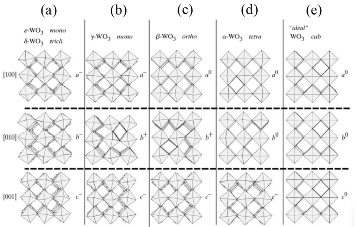
3Crystal Structures WO3 exhibits a perovskite-like structure based on corner and edge sharing of WO6 octahedra with O at the corner and W at the center of each octahedra.44 WO3 crystals go through structural transformations according to the sequence: tetragonal (> 740 °C) →
→ ) °C 43 − to 17 °C ( triclinic → ) 17 °C to 330 °C monoclinic ( → ) 330 °C to orthorhombic (740 °C
monoclinic (< −43 °C) as the temperature changes (Figure 2-2).44-47 Hexagonal WO3 is particularly (change in the optical absorption properties of a material as a function ochromism
to electr relevant
of the electrical bias applied). The electrochromism of WO3, first reported in 1979, benefits from its open tunnel structure and intercalation chemistry.48 In hexagonal WO3, three- and six-membered rings are formed by WO6 octahedra in the ab-plane and these octahedra are stacked by sharing the axial oxygen and form 4-coordinated square windows in the c-axis.45 Amorphous WO3 is built up of tightly bound (WO6)n ∙mH2O clusters with a large number of W=O and W-O-W bonds between the clusters. The porous structure of amorphous WO3 is enhanced by the corner or edge sharing octahedrons (3-8 membered rings network) forming clusters smaller than 20-30 Å.49,
50 Water molecules are easily filled in the open structure of amorphous WO3 films due to the ffects on the physical properties of have strong e
ter molecule a
W random packing of the clusters.
films and they can only partly removed by heating.51
Figure 2-2 Structural models for tungsten oxide: (a) low temperature monoclinic, triclinic; (b) room temperature monoclinic; (c) orthorhombic; (d) tetragonal and (e) simple cubic. (Reprinted with permission from Ref. 52, Copyright 2000, International Union of Crystallography)
Electronic band structure WO3 is an n-type semiconductor with bandgap Eg of about 2.6 -3.2 eV, function of the synthesis and processing conditions. Granqvist et al. calculated the density of states (DOS) for cubic WO3 (Figure 2-3).53 The results show that the O p states would form the valence band and W d states the conduction band; in addition, there would be considerable hybridization between the valence and the conduction bands. However, the value of Eg of 0.6 eV obtained from their calculations is quite different from the experimental results due to the fundamental limitations of local density approximation in semiconductor systems.54 For instance, amorphous WO3 with the
most distorted structure has Eg of ≈3.25 eV, whereas monoclinic WO3, in bulk form, has Eg of ≈ 2.6 eV at room temperature.55
Figure 2-3 DOS of cubic WO3. When energy is below 0 eV, filled states are found; empty states are found when energy is above 0 eV. (Reprinted with permission from Ref. 53, Copyright © 1996, American Physical Society)
Electrical conductivity (σ) For n-type metal oxide semiconductors, the electrical conductivity depends on the concentration of mobile electrons, which is mainly determined by the concentration of stoichiometric defects. Defects, such as oxygen vacancies, in the lattice of WO3 are able to increase σ by many orders of magnitude.56 Gillet et al. investigated WO3 conductivity variations as a function of temperature with different pressures of oxygen. The results indicated that the surface oxygen vacancies introduce donor levels in the gap and mobile electrons are produced by thermal activation. In addition, dopants57, microstructure characteristics (including grain size, nature of grain boundaries and specific crystalline phase) and film thickness also have a great influence on the conductivity. The electrical properties of WO3 are strongly dependent on the synthesis technique and growth conditions. For example, Vemuri et al. reported the effect of structure and size of nanocrystalline WO3 films on their electrical properties.58 They found that the lower conductivity of WO3 films treated at room temperature (RT) is due to their amorphous nature
and thus the conductivity increases with increasing substrate temperature because of the increasing crystalline nature and preferred orientation of the nanocrystalline WO3 films along (00L).58
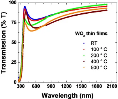
Optical properties The optical properties of WO3 in the visible region are dominated by the absorption threshold. When the photon energy is smaller than Eg, i.e. for wavelength λ longer than
hc/Eg, where h is the Planck constant and c is the speed of the light, the material does not absorb light. When the photon energy is equal to Eg, absorption from interband transitions will start to occur. For photon energies greater than the Eg, the light absorption coefficient α can be described:
𝛼ℎ𝜈 ∝ (ℎ𝜈 − Εg)𝜂
Where ν (= c/λ) is the photon’s frequency, h𝜈 is the photon’s energy and η is an exponent. For WO3, since the band gap is indirect (the crystal momentums of electrons and holes are not the same in the conduction band minimum and valence band maximum), the transitions are indirect and allowed, i.e. η = 2.53 Typical transmission spectra of WO3 are shown in Figure 2-4.
Figure 2-4 Transmission spectra of radio-frequency (RF) magnetron sputtered WO3 films on optical grade quartz substrates with different substrate temperatures (Reprinted with permission from Ref. 59, Copyright 2010, AIP Publishing LLC)