O
pen
A
rchive
T
OULOUSE
A
rchive
O
uverte (
OATAO
)
OATAO is an open access repository that collects the work of Toulouse researchers and
makes it freely available over the web where possible.
This is an author-deposited version published in :
http://oatao.univ-toulouse.fr/
Eprints ID : 19464
To link to this article :
DOI: 10.1109/TNS.2017.2710629
URL :
http://dx.doi.org/10.1109/TNS.2017.2710629
To cite this version : Zerarka, Moustafa and Austin, Patrick and Bensoussan,
Alain and Morancho, Frédéric and Durier, André TCAD simulation of the
Single Event Effects in normally-off GaN transistors after heavy ion radiation.
(2017) In: RADECS 2016, 19 September 2016 - 23 September 2016 (Bremen,
Germany).
Any correspondence concerning this service should be sent to the repository
administrator:
[email protected]
TCAD Simulation of the Single Event Effects
in Normally-
OFF
GaN Transistors
After Heavy Ion Radiation
M. Zerarka, P. Austin, A. Bensoussan, F. Morancho, and A. Durier
Abstract— Electrical behavior of commercial off-the-shelf
normally-off GaN power transistors under heavy ion irradiation is presented based on technology computer aided design numer-ical simulation in order to better understand the mechanism of single event effects (SEEs) in these devices. First, the worst case has been defined from the single event transient mechanism. Then, the decrease in the electric field observed after irradiation and the traps effect have been addressed. Finally, possible mech-anisms of SEE in these devices under heavy ion are proposed.
Index Terms— Efficient power conversion (EPC), gallium
nitride (GaN), heavy ion, HEMT, power transistor, radiation, single event effect (SEE), sensitive volume, simulation, technology computer aided design (TCAD).
I. INTRODUCTION
T
HE normally-OFFgallium nitride (GaN) power transistor could be specifically an attractive candidate for space and aeronautic power applications, due to its high electron mobility with high power. The use of these devices in such environment cannot be ensured without careful consideration of the effects of radiation. Natural radiation environment is composed of particles of various nature and energy, such as heavy ions, which can cause the destruction of these devices. Single event effects (SEEs) are one of the most menacing mechanisms, which could cause normally-OFFGaN power devices to fail in space systems. Few studies have been carried out to understand SEE in normally-OFFGaN power transistors.The objective of this paper is to investigate, by 2-D tech-nology computer aided design (TCAD) simulation, the mech-anism of the failure induced by heavy ion irradiation on com-mercial normally-OFF GaN power transistors [from Efficient Power Conversion (EPC)] in order to better understand the electrical behavior after irradiation, to define the sensitive
Manuscript received October 14, 2016; revised December 15, 2016; accepted May 24, 2017. Date of publication June 1, 2017; date of current version August 15, 2017. The paper is a part of the research done at Institut de Recherche et Technologie (IRT Saint Exupéry), Toulouse, France. The simulations were made at Laboratoire d’Analyse et d’Architecture des Systèmes — Centre National de la Recherche Scientifique (LAAS-CNRS). The study was conducted in the frame of Electronic Robustness contract Project sponsored by several funding partners (mains: Agence Nationale de la Recherche, Airbus, Thales Alenia Space France, LAAS-CNRS).
M. Zerarka, A. Bensoussan, and A. Durier are with the Institut de Recherche et Technologie Saint Exupery, 31432 Toulouse, France (e-mail: [email protected]).
P. Austin and F. Morancho are with the UPS and LAAS-CNRS, Université of Toulouse, 31077 Toulouse, France.
Color versions of one or more of the figures in this paper are available online at http://ieeexplore.ieee.org.
Digital Object Identifier 10.1109/TNS.2017.2710629
volume, and to suggest an explanation of the mechanism of SEEs for these devices.
Heavy ions inducing destructive failures have been exten-sively studied in RF normally-ONHEMT. Most previous work has been focused on the effects of protons, neutrons, and elec-trons. The failure generated by the protons in the AlGaN/GaN HEMT was first examined by Cai et al. [1] showing the decrease in the dc current and in the transconductance for different proton fluencies. Similar studies on irradiation of protons at different energies [2], [3] show that the GaN devices are extremely hardened to radiation and that the energy of the proton has a significant effect on the amount of defects created in the 2DEG of the HEMT because of differences in the loss of nonionizing energy [4], [5]. Several works also explain the shift of electrical characteristics before and after irradiation [6]– [8].
Furthermore, in RF normally-ONHEMTs, Onada et al. [9] find that the largest enhanced charge occurs when ions strike the gate electrode. Other studies of normally-ONRF HEMTS suggested that the largest enhanced charge occurs when ions strike between the gate and the drain [10], [11].
In the literature, a few studies address phenomena gen-erated by heavy ions in commercial off-the-shelf (COTS) power GaN transistors. Bazoli et al. [12] show that COTS GaN transistors (RT240PD, 70V) are not sensitive to single event burnout (SEB) under neutron and heavy ion irradiations tests; however, a phenomenon similar to Single Event Gate Rupture (SEGR) was observed in these devices although no oxide is under the gate. They supposed that the defects created in AlGaN layers by incident particles could be the origin of the gate insulation. They confirm that GaN transistors are less sensitive to SEB than MOSFETs. Recently, different generations of this GaN technology (EPC) have been tested under heavy ion irradiation. Scheick [13] assumes that the critical region seems to be near the edge of the gate on the drain side. The lot-to-lot variance that has been taken into account appears to be a very significant parameter [13]. Other results consider that these devices are not as robust as expected and show that normally-OFFpower GaN HEMTs are affected by a significant charge amplification mechanism [9], [14]. These latter consider that the mechanism of enhancement charge collection is associated with bipolar and back-channel effects.
Regarding simulation results, they are extremely rare in the literature due to the prematurity of this technology that remains
Fig. 1. Cross sectional view of the active region of the GaN EPC 2019 transistor.
Fig. 2. Experimental (datasheet) and simulated ID(VGS) transfer
character-istic of the 200 V EPC2019 GaN HEMT.
uncontrolled even by manufacturers (epitaxy limited, defects, and dislocations). Predictive approach of mobility and traps effect has been proposed in [15] to explain the degradation of performance characteristics in RF AlGaN/GaN HEMTs; they propose that a virtual gate effect is the cause of the increase in critical voltage and increased reliability. To our knowledge, any studies address simulation of SEE generated by heavy ions in COTS normally-OFF power GaN transistor and experimental results could not give a clear explanation of these failure mechanisms. Therefore, predictive modeling of these devices is strongly necessary; this is the aim of this paper.
II. TESTVEHICLES
A reverse engineering was carried out on samples GaN EPC2019ENG 200V (procured in 2014) in order to define the technological parameters of these devices. Fig. 1 gives a cross sectional view of the EPC2019 GaN HEMT that will be simulated. The structure consists of a substrate [silicon (Si)], a nucleation region comprising different AlGaN layers with aluminum rates gradually decreasing, an unintentional doped GaN buffer layer, an AlGaN barrier layer, a p-doped GaN layer [16], and a SiN passivation layer.
Despite a detailed constructional analysis, some parameters always remain unknown such as intentional and unintentional doping materials and level of doping concentrations, car-rier mobility, concentration, and energy of traps. However, it is necessary to first validate the physical and geometrical parameters obtained thanks to the technology analysis of EPC2019 transistor and calibrate by simulation those lacking,
Fig. 3. Schematic of simulation of heavy ion tracks impacting on normal incidence on the device from front and back side.
Fig. 4. Evolution of the drain current as a function of time after heavy ion impact for different LET (pC/µm) from the front side (x = 5 µm) at
VDS= 200 V in theOFF-state [27].
based on the experimental electrical characteristics of the device. Simulations were carried out with Sentaurus TCAD simulator [17]. The transport model used in simulation is the drift-diffusion model, and the current density under this model is described by the relation as follows:
j n = −qnµn∇8n,j = qpµ∇8p (1) where n and p are electron and hole concentrations, respec-tively; µn and µp are the electrons and holes mobility, respectively; 8n and 8p are the respective quasi-Fermi levels. GaN models are perfectly detailed in [18] and [17]. The key parameters of our calibration are the doping and traps concentrations. The most important concentrations are: an unintentional doping density of acceptor type of 1 × 10¹⁶
cm−3 in the GaN layer; an unintentional doping density of
donor type of 1 × 1016 cm−3 in the AlGaN layer; and an
acceptor trap density of 5 × 1017 cm−3 with energy level
of 0.45 eV from the conduction band. As shown in Fig. 2, the ID(VGS) transfer characteristics of the simulated structure
Fig. 5. Evolution of the drain current as a function of time after heavy ion impact between gate and drain electrode (x = 5µm) for different source–drain biases from the front side with 2 µm of track length and LET of 1 pC/µm [27].
EPC2019 devices have been tested to determine the actual values of their breakdown voltage: the same component may exhibit different values (between 200 and 420 V) when test was repeated under the same conditions. This can be explained by the heating effect which changes the traps energy after each test, increasing the trap-assisted gate tunneling mecha-nism [20]. In simulation, the value of the breakdown voltage was adjusted to 450 V by fitting some key parameters as the traps in the GaN buffer layer and their energy level.
III. CONDITIONS OFSIMULATIONSWITHHEAVYION
After calibrating the simulator, we simulated the struc-ture with different conditions as shown in Fig. 3. The aim is to investigate how the commercial power normally-OFF
GaN switch behaves at different conditions of heavy ion irradiation (position of tracks, range, and source–drain bias), while trying to find the most critical conditions for SEE and to localize the sensitive volume showing the highest change in residual electric field or trap density after irradiation simulation. These conditions have been also presented in our previous works in order to determine the sensitive volume in Si power devices (Vertical Diffused metal oxide semiconductor and transistor bipolaire à grille isolée) [21], [22].
In the first step, we studied the case of ions vertically generated in the volume of the cell of EPC2019, with track lengths of 2 µm generated at different x positions [see Fig. 3 (solid arrow)]. The objective is to determine the sensitive volume.
In the second step, we simulated the impact of ions pen-etrating from the front side with different track lengths. The case of ions penetrating from the backside was also studied [see Fig. 3 (dashed arrow)]. For these steps, all simulations were performed in the OFF-state, at the same source-drain bias corresponding to 90% of the breakdown voltage Vbr.
We also simulated these structures with different source-drain biases (40, 200, 300, and 400 V) in the OFF-state.
The ionizing impact is simulated by a function allowing the generation of electron–hole pairs in a specific area of
Fig. 6. Evolution of ID, IS, IG, and VGSas a function of time after heavy
ion impact from the front side at VDS= 200 V in blocking state [27].
the structure. The generation rate of the created charges is described by spatial and temporal Gaussian functions [17]. The track radius is set to 0.05 µm, the initial time of the charge generation is 3 × 10⁻¹³ s, and the temporal Gaussian
function width is 2 × 10⁻¹²s. Detailed work on the modeling
of the ion track charge and energy distribution can be found in [23] and [24].
IV. SIMULATIONRESULTS ANDDISCUSSION A. Single Event Transient Mechanism
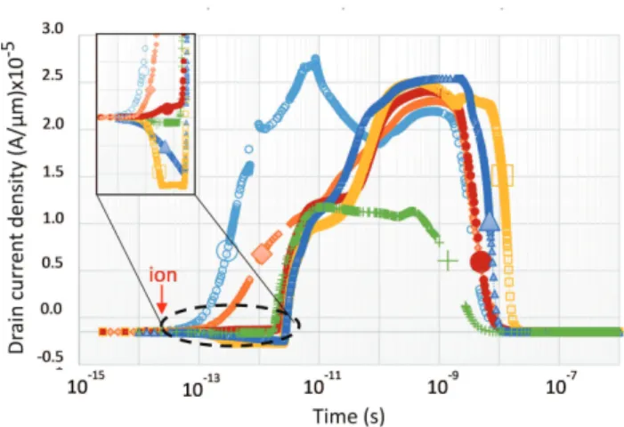
Results in Figs. 4 and 5 show the evolution of the drain current as a function of time after heavy ion impact for different Linear energy transfers (LETs) from the front side. Whatever the conditions (LET and bias), all failures are transient and the triggering current cannot be sustained. This transient current represents the charge enhancement. Gen-erally, in HEMTs heterostructures, the charge enhancement mechanism is associated with two mechanisms: the bipolar and the back-channel effects. When heavy ion crosses the active area of the device, electron–hole pairs are generated, creating ionized plasma. Electrons flow toward the drain contact with high mobility, leading to an excess of holes in the GaN buffer layer, thus electrons are injected to compensate from the source, leading to the switch of the parasitic bipolar transistor [9], [25], [26]. The second charge enhancement mechanism is due to the positive charge accumulation under the gate that helps to reduce the potential barrier between the source and the channel allowing the injection of electrons from the source to the drain via the channel [9], [25], [26]. In Fig. 4, the transient drain current reaches a saturation value for LET of 1 pC/µm. These LET correspond to the maximum of charge which can be generated in the GaN buffer region at 200 V. From this amount of charge, the amplitude of transient drain current does not increase anymore, whatever the LET value is set. This phenomenon value depends especially on the bias voltage but not on the ion energy or range. Fig. 5 confirms that the amplitude values of the drain current can be multiplied by a factor 6 when increasing the drain–source bias voltage for the same charge deposited by the heavy ion [27].
Fig. 7. Evolution of the drain current as a function of time after heavy ion impact for different x positions from the front side at V DS = 200 V in the
OFF-state (see Fig. 3 to refer to x position).
Fig. 6 explains the mechanism of the transient current after the heavy ion strike. It shows that only the self-polarization of the gate by the hole current coming from ionized plasma leads to turn-ON the device. The majority of the electron current coming from the source passes through the channel, reducing the electron current flowing through the GaN buffer or the whole structure to compensate for the accumulated holes, which minimizes the parasitic bipolar effect. The satura-tion value depends especially on the bias and not on the energy or range of the ion. Fig. 5 confirms that the amplitude values can be multiplied by increasing the drain–source bias voltage for the same charge deposited by the heavy ion. Since the ionization coefficients and detrapping are exponentially related to the electric field via Poisson’s equations, the rise in the polarization increases the detrapping and the generation of electron–hole pairs, increasing the hole current in the gate, leads to more charge enhancement [27]. This is similar to the direct characteristic ID(VDS): the saturation drain current
increases with the increase in gate bias (VGS).
If we compare with MOSFET device behavior under irradi-ation modeling, the proposed mechanism involves avalanche effect combined to the parasitic bipolar transistor structure, both providing charges to each other [28]. When considering GaN normally-OFFstructure under irradiation, we assume that the transient triggering of parasitic bipolar structure cannot maintain a drain current avalanche thus avoiding burnout failure.
B. Sensitive Volume
One can see, from the analysis of Fig. 7, that the transient current is less important when heavy ion is present in the source region, since outside of the space charge region, the tracks require a much larger LET. While there is no significant change in amplitude for all traces generated in the depletion region between the gate and drain, the change in shape is more evident. The tracks that are close to the source and gate have a negative current, just after the impact, and the tracks that are close to the drain do not have this negative
Fig. 8. Evolution of the drain current as a function of time after heavy ion impact for different track lengths (µm) from the front side at VDS= 200 V in blocking state.
current [see Fig. 7 (zoom)]. We do not know exactly the origin of this negative current. We think that, when heavy ion is generated close to the gate, excess of holes is close to the source which allows inducing a bipolar mechanism before back-channel effects. However, when heavy ion is generated close to the drain, excess of holes is close to the drain and relatively far from the source: holes need more time to reach the gate or source region and recombine partially. The bipolar mechanism needs high amount of holes unlike the mechanism of the back channel which can be activated with a small amount of charge. Heavy ion generated close to the drain will activate only the back channel and all the electrons will pass through the channel, which explains its relative speed triggering compared with the ones generated close to the gate region.
Figs. 8 and 9 show the evolution of the drain current as a function of time after heavy ion impact for different track lengths from the front side and back side, respectively. The transient drain current reaches a saturation value for ranges of 0.2 µm. These ranges correspond to 20% of the depth of the GaN buffer region at 200 V. From this penetration, the amplitude of transient drain current is constant, whatever the range value. The saturation value depends especially on the bias voltage and not on the energy or range of the ion. Fig. 5 confirms that the amplitude values are strongly related to the increasing drain–source bias voltage for the same charge deposited by the heavy ion, while keeping the same shape.
The comparison of Fig. 8 (front side) and Fig. 9 (back-side) shows that the sensitive case is observed when the heavy ion comes from the front side, especially for the lowest ranges. The tracks, which penetrate toward the channel area (range = 3. µm) from the back side, induce the same transient drain current of the one coming from the front side with a range of 0.2 µm. The first trigger time is slower for small ranges. The transient current does not occur in the same time scale as seen in the case of ion injected on the front side.
Fig. 9. Evolution of the drain current as a function of time after heavy ion impact for different track lengths ( µm) from the back side at VDS= 200 V in blocking state.
Fig. 10. Electric field decrease after radiation at different track positions (hor-izontal section at C1 of Fig. 3).
C. Effect of Radiation on the Electric Field
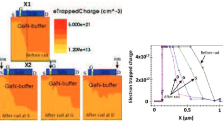
The decrease in the electric field before and after the impact of heavy ion has been analyzed. Fig. 10 shows a systematic observation of the electric field in the simulated structures before and after heavy ion irradiation at 300 V. Results show that the electric field significantly decreases along the structure after radiation.
Fig. 11 indicates that the density of traps has a significant effect on the peak of the electric field observed after radiation. Since the detrapping is more important in the ions strike close to the gate electrode, the electric field will decreased much more in this area. This may explain the increase in breakdown voltage observed in [29]. In contrast, for RF HEMT, Patrick et al. [15] suggest that the trap density in GaN buffer does not have a significant effect on the peak of the electric field observed after irradiation. They explain that it could be due to postradiation traps formed in the
Fig. 11. Electron trapped charge before and after heavy ion radiation (vertical section from x1 to x2).
Fig. 12. Electric field decrease with different track lengths (horizontal section at C1 of Fig. 3) (see Fig. 3 to refer to y position).
AlGaN/Nitride interface, not to postradiation traps formed in the GaN buffer layer; a similar explanation was adopted in [30] in their radiative tests (2 MeV protons) on AlGaN/GaN HEMT with different substrates (Si, SiC, and Al2O3). This difference
reveals that the trap density in the GaN buffer layer has a more significant effect in power switch HEMTs than in RF HEMTs. As in the case of different x positions, the decrease in the electrical field after irradiation can better demonstrate the effect of each track length. Fig. 12 shows a systematic observation of the electric field in the simulated structures before and after heavy ion radiation at different depths of penetration for ion coming from the front side. The same large decrease appears around the ion impact position near the gate electrode (x = 5µm), whatever the track length is. Here, the range has a little effect since the track position is located near the end of the depletion region with fewer traps; consequently, the detrapping effect on the electric field is the same. However, the decrease on the drain side is very important only when the heavy ion penetrates 40% of the GaN buffer layer (range = 0.4 µ). The most significant electric field decrease is occurring at 0.8 µm of range, which corresponds
Fig. 13. Evolutions of displacement drain current IDDand VDSas a function
of time after heavy ion impact from the front side at V DS = 400 V in blocking state (without impact ionization model) [27].
Fig. 14. Evolutions of displacement drain current IDDand VDSas a function
of time after heavy ion impact from the front side at V DS = 400 V in blocking state (with impact ionization model) [27].
to 80% of the depth of GaN buffer layer and from this range, the electric field decrease remains nearly the same.
D. Proposed Scenarios of Single Event Effect
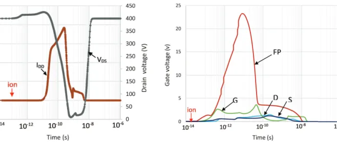
1) First Scenario (Burnout): : The plasma generated by a heavy ion can occupy a large part of this small device inducing a big dE/dt, which gives a large displacement current. Simulation shows that this current is collected by the elec-trodes. These simulated data, could provide possible scenarios of SEE in normally-OFFGaN power transistors under heavy ion. The displacement current, caused by the abrupt change of VDS or VDG immediately after heavy ion impact, is shown
in Fig. 13 without impact ionization model and in Fig. 14 with impact ionization model. Concerning the first case (with-out impact ionization model), the displacement current does not appear immediately after the ion impact: this current increase with the transient drop of VDS, and decreases when VDS ascends. On the other side, when the impact ionization
Fig. 15. Evolution of the gate voltage as a function of time after an heavy ion radiation for different x positions (S: source, G: gate, D: drain, FP) from the front side at V DS = 200 V in blocking state.
model is considered, a very important displacement current (0.1 A/µm) is observed, nearly 1000 times larger than the current simulated without considering the impact ionization model. This current appears just after the ion hits the front side simultaneously to the VDS increase [see Fig. 14 (zoom)]
and before the drop voltage. Even if this displacement current, caused by the avalanche phenomenon, occurs during a very short time, we assume that this mechanism is probably the origin of SEE in these devices since usually the avalanche phenomenon in the real components is not reversible. We also assume that this mechanism can cause a current filamentation as being responsible of destructive breakdown. This mecha-nism is observed only in the highest VDS over than 2000V.
For VDS less than 200 V, the impact ionization mechanism
has no effect. Furthermore, the very high current densities and conductivity of the GaN generated by the avalanche is assumed not to be supported by its limited thermal capacity and thermal conductivity (related to the Si substrate limitation); as a consequence, this increases the risk of thermal runaway [27]. The displacement current in Si devices was sometimes related to the triggering of the parasitic thyristor as the case of triode for alternating current, the combination of the high [dV/dt] and the presence of the stored charge can lead to the undesirable turn-ON and to the destructive failure of the thyristor without external gate drive current [31]. In the case of a GaN transistor, this possibility is very unlikely.
2) Second Scenario (Dielectric Rupture):: Results in Fig. 15 could also provide another possible scenario of SEE in normally-OFF GaN power transistors under heavy ion. Despite this similarity in drain current behavior between different track positions as shown in Fig. 7, there is an important difference in the gate voltage. Fig. 15 shows that the transient gate voltage is much more important when heavy ion is present in the field plate (FP) edge. The gate voltage value could exceed 22 V when heavy ion particles are generated in this region, exactly in the edge of the FP. This voltage gives a high electric field of 2.2 MV/cm at the
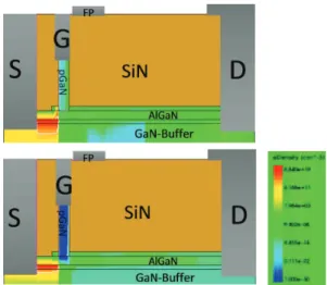
Fig. 16. Impact ionization when a heavy ion strikes at the field plate edge (left) and at the gate (right).
Fig. 17. Leakage current before (top) and after (bottom) radiation.
thickness of the passivation film (Si3N4) between the gate
and the FP (0.1 µm), which is close to the capacitance of this layer, the mean failure electric field for Si3N4 being
2.9 MV/cm [32]. Few studies address ion damage in Si3N4,
Wrobel [32] suggested that the density of electron–hole plasma along with the heavy ion track in the dielectric induces a conductive “pipe” that can be a discharge path of energy stored on the capacitor. We suppose that this hypothesis is possible in this case when heavy ions and this high transient gate voltage are applied together.
Fig. 15 shows a drawing of the evolution of the gate voltage as a function of time after heavy ion impact for different x positions (S: source, G: gate, D: drain, FP) from the front side at VDS = 200 V in OFF-state. From these results, we observe that susceptible region which may lead to the dielectric rupture can be located at the FP edge. This contact is the nearest to the drain contact and creates the highest electrical stress, which can exceed the edge gate stress on the
drain side. Therefore, impact ionization mechanism and related multiplication phenomena are enhanced when a heavy ion strikes under the FP edge rather than the other track positions as shown in Fig. 16, that compare the two critical positions, gate and FP. Several studies of SEGR in power MOSFETs have shown that the gate leakage current resulting from the ion impact has been increasing rapidly with the exposure time under the beam. This increase can lead to the breakdown of the gate oxide (SiO2) in most cases [27].
Other studies have shown that the dielectric breakdown was mainly affected by pre existing damage [33] and SEGR could also be triggered by ions crossing only the epitaxy without reaching the oxide [34]. Fig. 17 shows a significant increase in electron density after single heavy ion track, especially in the p-GaN layer, the interface p-GaN/Si3N4, and SiN/AlGaN
layer [Fig. 17 (green)]. This promotes the trap/defect-assisted gate tunneling and increases the leakage current at the gate after irradiation. We assume that the accumulation of this electron density after irradiation for longer ion exposures can considerably increase the risk of the degradation of Si3N4and
its rupture like SEGR in MOSEFT or triggering a burnout initiated by leakage current.
V. CONCLUSION
Using TCAD simulation, we explain the mechanism of the transient current after the heavy ion strike in normally-OFF
GaN power transistors. The self-polarization of the gate by hole current coming from ionized plasma leads to transient turn-ON the device. We assume that the minor effect of the parasitic bipolar transistor in such devices induces that the triggering is always reversible and avalanche drain current cannot be maintained. The worst case at 200 V in commercial normally-OFF GaN power transistors is related to an ion coming from the front side, striking next to the FP edge and crossing more than 20% of the GaN buffer layer. The most significant electric field decrease observed after radiation is occurring at the drain side. The density of traps in GaN buffer layer has a significant effect on the decrease in the electric field in contrast to RF HEMT devices. This may explain the increase in breakdown voltage observed in the literature.
A possible mechanism of SEE in these devices under heavy ion has been proposed: a heavy ion can induce a huge displacement current (0.1 A/µm) caused by the avalanche phe-nomenon in high voltage and the abrupt change in VDSor VDG
immediately after heavy ion impact is probably the origin of SEE. Another possible scenario supposes that the origin of SEE in normally-OFF GaN power transistors is probably the rupture of the dielectric passivation layer (SiN) and this susceptible configuration, which may lead to dielectric rupture, occurs when heavy ion strikes near the FP edge.
ACKNOWLEDGMENT
Constructional analysis on the GaN technology was con-ducted by SERMA technologies under Thales Alenia Space contract.
REFERENCES
[1] S. J. Cai et al., “Annealing behavior of a proton irradiated AlxGa1−xN/GaN high electron mobility transistor grown by MBE,”
IEEE Trans. Electron Devices, vol. 47, no. 2, pp. 304–307, Feb. 2000. [2] B. Luo et al., “DC and RF performance of proton-irradiated AlGaN/GaN high electron mobility transistors,” Appl. Phys. Let., vol. 79, no. 14, pp. 2196–2198, 2001.
[3] H.-Y. Kim, J. Kim, L. Liu, C. F. Lo, F. Ren, and S. J. Pearton, “Effects of proton irradiation energies on degradation of AlGaN/GaN high electron mobility transistors,” J. Vac. Sci. Technol. B, Microelectron. Process.
Phenom., vol. 30, no. 1, p. 012202, 2012.
[4] G. P. Summers, E. A. Burke, P. Shapiro, S. R. Messenger, and R. J. Walters, “Damage correlations in semiconductors exposed to gamma, electron and proton radiations,” IEEE Trans. Nucl. Sci., vol. 40, no. 6, pp. 1372–1379, Dec. 1993.
[5] J. R. Srour, C. J. Marshall, and P. W. Marshall, “Review of displacement damage effects in silicon devices,” IEEE Trans. Nucl. Sci., vol. 50, no. 3, pp. 653–670, Jun. 2003.
[6] X. Hu et al., “The energy dependence of proton-induced degradation in AlGaN/GaN high electron mobility transistors,” IEEE Trans. Nucl. Sci., vol. 51, no. 2, pp. 293–297, Apr. 2004.
[7] T. Roy et al., “Process dependence of proton-induced degradation in GaN HEMTs,” IEEE Trans. Nucl. Sci., vol. 57, no. 6, pp. 3060–3065, Dec. 2010.
[8] Y. S. Puzyrev, T. Roy, E. X. Zhang, D. M. Fleetwood, R. D. Schrimpf, and S. T. Pantelides, “Radiation-induced defect evolution and electrical degradation of AlGaN/GaN High-Electron-Mobility transistors,” IEEE
Trans. Nucl. Sci., vol. 58, no. 6, pp. 2918–2924, Dec. 2011.
[9] S. Onoda et al., “Enhanced charge collection by single ion strike in AlGaN/GaN HEMTs,” IEEE Trans. Nucl. Sci., vol. 60, no. 6, pp. 4446–4450, Dec. 2013.
[10] S. DasGupta, D. McMorrow, R. A. Reed, R. D. Schrimpf, and J. B. Boos, “Gate bias dependence of single event charge collec-tion in AlSb/InAs HEMTs,” IEEE Trans. Nucl. Sci., vol. 57, no. 4, pp. 1856–1860, Aug. 2010.
[11] S. Onoda, T. Makino, S. Ono, S. Katakami, M. Arai, and T. Ohshima, “Spatial, LET and range dependence of enhanced charge collection by single ion strike in 4H-SiC MESFETs,” IEEE Trans. Nucl. Sci., vol. 59, no. 4, pp. 742–748, Aug. 2012.
[12] S. Bazzoli, S. Girard, Ferlet-Cavrois, J. Baggio, P. Paillet, and O. Duhamel, “SEE sensitivity of a COTS GaN transistor and silicon MOSFETs,” in Proc. RADECS, Deauville, France, Sep. 2007, pp. 1–5. [13] L. Scheick, “Determination of single-event effect application require-ments for enhancement mode gallium nitride HEMTs for use in power distribution circuits,” IEEE Trans. Nucl. Sci., vol. 61, no. 6, pp. 2881–2888, Dec. 2014.
[14] C. Abbate et al., “Experimental study of single event effects induced by heavy ion irradiation in enhancement mode GaN power HEMT,”
Microelectron. Rel., vol. 55, nos. 9–10, pp. 1496–1500 Aug./Sep. 2015. [15] E. Patrick et al., “Modeling proton irradiation in AlGaN/GaN HEMTs: Understanding the increase of critical voltage,” IEEE Trans. Nucl. Sci., vol. 60, no. 6, pp. 4103–4108, Dec. 2013.
[16] A. Y. Polyakov, S. J. Pearton, P. Frenzer, F. Ren, L. Liu, and J. Kim, “Radiation effects in GaN materials and devices,” J. Mater. Chem. C, vol. 1, no. 5, pp. 877–887, Feb. 2013.
[17] Sentaurus TCAD Tools, Synopsys, Mountain View, CA, USA, 2013.
[18] J. C. Freeman, “Basic equations for the modeling of gallium nitride (GaN) high electron mobility transistors (HEMTs),” NASA, New York, NY, USA, Tech. Rep. NASA/TM-2003-211983, Feb. 2003. [Online]. Available: http://gltrs.grc.nasa.org
[19] Datasheet of EPC2019, accessed on 2013. [Online]. Available: http://epcco.com/epc/496Portals/0/epc/documents/datasheets/EPC2019_ datasheet.pdf
[20] G. Xie, E. Xu, B. Zhang, and W. T. Ng, “Study of the breakdown failure mechanisms for power AlGaN/GaN HEMTs implemented using a RF compatible process,” Microelectron. Rel., vol. 52, no. 6, pp. 964–968, Jun. 2012.
[21] M. Zerarka, P. Austin, and M. Bafleur, “Comparative study of sen-sitive volume and triggering criteria of SEB in 600 V planar and trench IGBTs,” Microelectron. Rel., vol. 51, nos. 9–11, pp. 1990–1994, Sep./Nov. 2011.
[22] M. Zerarka, P. Austin, G. Toulon, F. Morancho, H. Arbess, and J. Tasselli, “Behavioral study of single-event burnout in power devices for natural radiation environment applications,” IEEE Trans. Electron
Devices, vol. 59, no. 12, pp. 3482–3488, Dec. 2012.
[23] H. Dussault, J. W. Howard, Jr., R. C. Block, M. R. Pinto, W. J. Stapor, and A. R. Knudson, “Numerical simulation of heavy ion charge generation and collection dynamics,” IEEE Trans. Nucl. Sci., vol. 40, no. 6, pp. 1926–1934, Dec. 1993.
[24] H. Dussault, J. W. Howard, R. C. Block, M. R. Pinto, W. J. Stapor, and A. R. Knudson, “The effects of ion track structure in simulating single event phenomena,” in Proc. RADECS, Saint-Malo, France, Sep. 1993, pp. 509–516.
[25] D. McMorrow, A. R. Knudson, J. B. Boos, D. Park, and J. S. Melinger, “Ionization-induced carrier transport in InAlAs/InGaAs high elec-tron mobility transistors,” IEEE Trans. Nucl. Sci., vol. 51, no. 5, pp. 2857–2864, Oct. 2004.
[26] D. McMorrow et al., “Charge-enhancement mechanisms of GaAs field-effect transistors: Experiment and simulation,” IEEE Trans. Nucl. Sci., vol. 45, no. 3, pp. 1494–1500, Jun. 1998.
[27] M. Zerarka, P. Austin, A. Bensoussan, F. Morancho, and A. Durier, “TCAD simulation of the single event effects in normally-off GaN tran-sistors after heavy ion radiation,” in Proc. RADECS, Bremen, Germany, Sep. 2016.
[28] A. Luu “Méthodologie de prédiction des effets destructifs dus à l’envi-ronnement radiatif naturel sur les MOSFETs et IGBTs de puissance,” Ph.D. dissertation, Paul Sabatier Univ., Toulouse, France, 2009. [29] S. J. Pearton, Y.-S. Hwang, and F. Ren, “Radiation Effects in
GaN-Based High Electron Mobility Transistors,” JOM, vol. 67, no. 7, pp. 1601–1611, Mar. 2015.
[30] T. J. Anderson et al., “Substrate-dependent effects on the response of AlGaN/GaN HEMTs to 2-MeV proton irradiation,” IEEE Electron
Device Lett., vol. 35, no. 8, pp. 826–828, Aug. 2014.
[31] B. J. Baliga, Fundamentals of Power Semiconductor Devices. Raleigh, NC, USA: Springer, 1995, pp. 730–732.
[32] T. F. Wrobel, “On heavy ion induced hard-errors in dielectric structures,”
IEEE Trans. Nucl. Sci., vol. 34, no. 6, pp. 1262–1268, Dec. 1987. [33] D. M. Fleetwood and N. S. Saks, “Oxide, interface, and border traps in
thermal, N2O, and N2O-nitrided oxides,” J. Appl. Phys., vol. 79, no. 3,
pp. 1583–1594, 1996.
[34] D. Peyre et al., “SEGR study on power MOSFETs: Multiple impacts assumption,” IEEE Trans. Nucl. Sci., vol. 55, no. 4, pp. 2181–2187, Aug. 2008.

![Fig. 6. Evolution of I D , I S , I G , and V GS as a function of time after heavy ion impact from the front side at V DS = 200 V in blocking state [27].](https://thumb-eu.123doks.com/thumbv2/123doknet/3093980.87629/4.892.108.405.132.408/fig-evolution-function-time-heavy-impact-blocking-state.webp)