HAL Id: pastel-00002930
https://pastel.archives-ouvertes.fr/pastel-00002930
Submitted on 28 Jul 2010HAL is a multi-disciplinary open access
archive for the deposit and dissemination of sci-entific research documents, whether they are pub-lished or not. The documents may come from teaching and research institutions in France or abroad, or from public or private research centers.
L’archive ouverte pluridisciplinaire HAL, est destinée au dépôt et à la diffusion de documents scientifiques de niveau recherche, publiés ou non, émanant des établissements d’enseignement et de recherche français ou étrangers, des laboratoires publics ou privés.
Resonance Plasma Enhanced Chemical Vapor
Deposition MDECR-PECVD.
Bicher Haj Ibrahim
To cite this version:
Bicher Haj Ibrahim. The deposition of multilayer and gradient index thin films by Matrix Distributed Electron Cyclotron Resonance Plasma Enhanced Chemical Vapor Deposition MDECR-PECVD.. Physics [physics]. Ecole Polytechnique X, 2007. English. �pastel-00002930�
THÈSE
présentée pour obtenir le grade de
DOCTEUR DE L’ECOLE POLYTECHNIQUE Spécialité : Physique.
Bicher HAJ IBRAHIM
Dépôt de couches minces à saut et gradient d’indice
par plasma en résonance cyclotron
The deposition of multilayer and gradient index thin films
by MDECR-PECVD
Date de soutenance : le 12 avril 2007
Jury
Bernard AGIUS
Président
Jean-Eric BOURÉE
Directeur de thèse
Pavel BULKIN
Co-directeur
Mireille COMMANDRÉ
Frédéric FERRIEU
Rapporteur
Agnès GRANIER
Rapporteur
Jean-Christophe ROSTAING
LABORATOIRE DE PHYSIQUE DES INTERFACES ET COUCHES MINCES, CNRS UMR 7647 ÉCOLE POLYTECHNIQUE
“The Virtue of the man is to discipline his mind.”
Friedrich Nietzsche
I offer this work to :
all those who participated from near or far
in the orientation of my life and my mind.
Especially, to the soul of my father,
to my mother,
to my fiancée,
to my sisters and their husbands,
to my beloved nephews and nieces,
to all my teachers during my studies,
I would thank for this work :
- M. Bernard Drévillon Director of Laboratoire de Physique des Interfaces et des Couches Minces at Ecole Polytechnique who received me in his laboratory, and supported me during the PhD.
- M. Jean Eric BOURÉE the director of my PhD., who helped me scientifically, and took care of the advancement of the PhD.
- Special thanks to M. Pavel BULKIN for his daily help, his orientation was essential for me to improve and achieve this project. His know-how made me save time, and encouraged me to progress steadily.
- Miss Roelene BOTHA, my successor in the team, for her help during her internship and her thesis.
- M. Frédéric LIÈGE and M. Garry ROSE KITCHNER who installed the electronic equipments, and helped me to program the control of the different parts, and with whom I appreciated work and cooperation.
- M. Jean Luc MONCEL, M. Cyril JADAUD, M. Dominique CLÉMENT and M. Éléonor CARISTAN who installed the mechanical parts of the experiment, and who veiled on the security of the work.
- M. Grégory GIRARD, the previous PhD student for his support and advice during the beginning of the PhD.
- Mrs. Laurence CORBEL and Chantal GENESTE, for the administrative help and the good environment they installed in the laboratory.
- From Jobin-Yvon, Michel STHCAKOVSKY and Dmitri KOUZNETSOV. - Special acknowledgment to Pere ROCA i CABARROCAS, Dmitri DAINEKA,
Tatiana NOVIKOVA, Antonello DE MARTINO, Razvigor OSSIKOVSKI and Yvan BONNASSIEUX, for the interesting scientific explanation and cooperation.
- All the team of the Laboratory LPICM for the precious moments I passed with them : Quentin BRULIN, Céline BERNON, Ning NING, Martin FOLDYNA, Erik JOHNSON, Nans PHAM, Makrina ANASTASIADOU, Régis BISSON, Jérôme CHARLIAC, Arnaud-Julien GUILLEY, Gowtham MANOHARAN, Olivier GODDE, Laurent EUDE, Régis VANDERHAGHEN, Razvan NEGRU, Kim HYUN JONG, Alexei ABRAMOV, Yassine DJERIDANE, Costel-Sorin COJOCARU, Holger VACH, Laurent SCHWARTZ, Didier PRIBAT, Jean-Yves PAREY, Josiane MABRED, Dominique CONNE, Fatiha KAIL, Enric GARCIA-CAUREL, Dohyung KIM, Jérôme DAMON-LACOSTE, Marc CAHTELET, Van Diep BUI, Sami BEN-HATIT, Laurent PHILIPPE, Thien Hai DAO, Quang NGUYEN, Tran Thuat NGUYEN, Gregoriy DOLGONOS.
B. Haj Ibrahim The Deposition of Thin Films by MDECR-PECVD
Table of Contents
Introduction 1
Chapter 1 PECVD of Optical Thin Films 5
1.1 Requirements for Optical Thin Film Technology 5
1.1.1 The Design of Optical Thin Films 7
1.1.2 The Theory of Optical Thin Films: The Matrix Formalism 10
1.1.3 Thin Film Deposition 13
1.2 Principles of PECVD: Different Deposition Reactors 15
1.3 Range of Materials in PECVD 18
1.4 Control Techniques for Optical Material Deposition 20
1.4.1 Quartz Crystal Microbalance 20
1.4.2 Single Wavelength and Spectral Reflectometry 21
References 23
Chapter 2 High Density Plasma Sources 25
2.1 Plasma and Plasma Properties 26
2.2 Microwave Discharges and the ECR Effect 27 2.2.1 The Motion of a Charged Particle in an Electromagnetic Wave 27 2.2.2 The Larmor Radius and the ECR Effect 29
2.3 Low Pressure Microwave Reactors 31
2.3.1 Divergent ECR 32
2.3.2 Microwave Plasma Disk Reactors 33
2.3.3 Distributed ECR 34
2.3.4 Integrated Distributed ECR 35
2.3.5 Matrix Distributed ECR 36
References 38
Chapter 3 Implementation of an MDECR-PECVD Reactor: VENUS 41
3.1 Description and Construction 42
3.1.1 The Gas Panel, Mass Flow Controllers and Computer Control 45 3.2 Characterization of the Vacuum System and Process Parameter Range 49 3.2.1 Calculation of the Leak Rate and Residence Time 49 3.2.2 Radio Frequency Biasing of the Substrate 52 3.3 ECR Plasma Characterization by Optical Emission Spectroscopy 52
3.3.1 The Influence of SiH4 Flow 56
3.3.2 The Influence of Increased Microwave Power 57 3.3.3 The Influence of Biasing the Substrate 58 3.4. Nature of the Deposition Process in a HDP-PECVD Reactor:
Implications for Silica Deposition 59
3.4 Conclusion 62
B. Haj Ibrahim The Deposition of Thin Films by MDECR-PECVD
Chapter 4 Deposition of SiOxNy Optical Filters by MDECR-PECVD 67
4.1 Phase Modulated Ellipsometry 68
4.2 Characterization by Spectroscopic Ellipsometry 70 4.3 Characterization by FTIR Spectroscopy 74 4.4 The Influence of the Magnet Matrix Configuration 76 4.5 The Influence of the Applied Microwave Power on SiNx Deposition 81 4.6 The Influence of RF Substrate Biasing 83 4.7 The Feed-forward Deposition of Gradient Optical Filters 88 4.7.1 A Gradient Index AR Coating in the Visible Range 90 4.7.2 Rugate Filter Deposition and Side Lobe Suppression 92
4.7.2.1. Bovard’s model 93
4.7.2.2. Correlation of side lobe suppression between multilayer
and rugate filters 94
4.7.2.3. Comparison between sinusoidal layer and quintic layer 98
4.8 Conclusion 101
References 102
Chapter 5 Real-Time Control Using Multi-Channel Kinetic Ellipsometry 107
5.1 Kinetic Ellipsometry 108
5.1.1 Kinetic Ellipsometry Calibration 108
5.1.2 Influence of The Plasma Emission 110
5.2 Methods For Controlling Layer Thickness And Refractive Index 115
5.2.1 Trajectory control methods 115
5.2.1.1 Trajectory Distance Method 116
5.2.1.2 Trajectory Length Method 118
5.2.2 Direct Numerical Inversion Method 118
5.2.3 Real-time Least Square Fit 121
5.3 Examples of Optical Layer Control by Least Square Fit 122
5.3.1 Thickness Control of a Single Layer 122
5.3.2 Thickness Control of Two Layers HL 124
5.3.3 Thickness and Index Control of a Three Layer MHL AR Coating
for the Visible Range 127
5.7 Conclusion 129
References 130
Chapter 6 Summary and Conclusion 131
Appendix I : The Classical Lorentz Oscillator and Tauc-Lorentz Models 135
Appendix II : List of Publications 139
List of Figures
1.1 Most common types of optical depositions 9
1.2 Conventions of s and p polarizations 11
1.3 Representation of a multilayer stack 11
1.4 Thin film deposition techniques 14
1.5 Standard CVD tube reactor 15
1.6 Electron-molecule collisions in a plasma 16
1.7 A basic RF-PECVD reactor 17
1.8 Reflectance profile at 530 nm, for monitoring a M2HL visible AR coating 22 2.1 Motion of an electron and Larmor radius in a constant magnetic field 30 2.2 Trajectory of an electron under the ECR effect and the resulting increase
in the Larmor radius 30
2.3 Divergent ECR system with resonance locations as modeled in [12] 32
2.4 Example of a commercial Microwave Plasma Disc Reactor [17] 33 2.5 Divergent ECR plasma with magnet and antenna positions 34
2.6 The IDECR reactor Plasface [19] 35
2.7 MDECR line of antennas with ECR regions 36
2.8 ECR zone around an antenna’s magnet in an argon plasma 37
3.1 The reactor Venus during assembly 41
3.2 Schematic of reactor Venus 43
3.3 Schematic of antennas used in reactor Venus 43
3.5 Venus after construction 44
3.6 Gas distribution system of the reactor 45
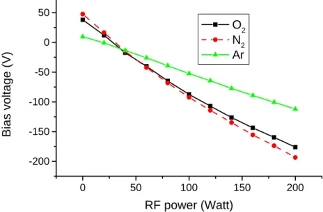
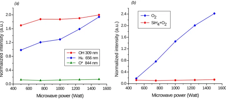
3.7 The structure of automation of the gas panel on the reactor 46 3.8 MFC’s response for transitions: (a) zero to maximal flow (b) one sccm 47 3.9 Manual control panel of gas flows, valves and microwaves 48 3.10 Loading of predefined gas flow files with the MFCs and DNET card status 48 3.11 Leak rate and pressure increase without pumping 50 3.12 Residence time and pumping speed of argon for a fully opened valve 51 3.13 Residence time and pumping speed of oxygen for a fully opened valve 51 3.14 Self-bias Voltage with increased power for different gases 52 3.15 Overlap of the emission cross sections and the EEDF 53 3.16 Optical ports used for OES measurements on the reactor Venus 54 3.17 Optical emission spectra for a SiNx deposition plasma 55 3.18 Optical emission spectra for a SiO2 deposition plasma 55 3.19 Optical emission intensities for H , O* and OH spectral lines taken at various
SiH4 gas flows 56
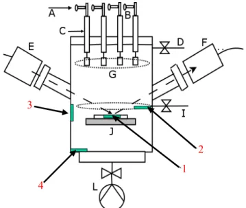
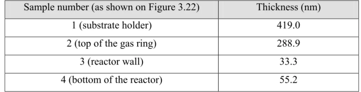
3.20 Optical emission intensities taken at various microwave powers 57 3.21 OES intensities taken at various RF bias Voltages on the substrate level 58 3.22 Sample arrangement for testing growth rate at different positions in the reactor 60 3.23 Gas distribution ring replaced by a capillary through which silane is injected
towards the substrate 60
3.24 The growth rate distribution for various silane flows 62 3.25 A summary of the different parts of the Venus reactor 64 4.1 Schematic view of a phase modulated ellipsometer 68
4.2 SiOxNy refractive index dispersion curves at various oxidants flow ratios 71 4.3 Refractive index versus oxidants ratio, at different SiH4 flows 72 4.4 Growth rate versus oxidants ratio, at two different SiH4 flows 73 4.5 FTIR spectra of SiOxNy, using a 5 sccm SiH4 flow 75 4.6 Comparison of SiOx deposited with pure O2 and with O2+N2 mixture 75 4.7 Magnetic field strength and ECR zones along a line connecting the midpoints
of two magnets 77
4.8 Simulation of the magnetic field distribution between two antennas: (a) Different directions of polarities, (b) Similar directions of polarities 77 4.9 Uniformity with changes in the magnet matrix configuration 79 4.10 Uniformity contours for the configurations shown in Figure 4.9 (a)-(c) 80 4.11 Variation of the refractive index and the growth rate of nitride layers
versus microwave power 82
4.12 Shift of Si-N peak with microwave power 82
4.13 Influence of RF biasing of the substrate holder on SiOxNy growth rate 83 4.14 FTIR measurement of SiNx at two different silane flows 84 4.15 SiOxNy index at 5 sccm SiH4 flow, with and without substrate biasing 85 4.16 FTIR measurement of SiNx at 5 sccm SiH4, with and without RF biasing 85 4.17 SiOxNy index at 10 sccm SiH4 flow, with and without substrate biasing 86 4.18 FTIR measurement of SiNx at 10 sccm SiH4, with and without RF biasing 87 4.19 SiOx deposited under different RF biasing conditions 87 4.20 Variations in the O2, N2 flows and refractive index when depositing a linear
gradient index layer 89
4.22 Index and rate profile for a gradient index AR coating 91
4.23 Transmission of a gradient index AR coating 91
4.24 Index profile of a rugate filter and a multilayer mirror at 619.5 nm (2 eV)
versus optical thickness 94
4.25 Reflectance of different multilayer mirrors for a glass substrate in air
medium: (a) (HL)NH stack. (b) 0.5HL(HL)N0.5H. (c) 0.5L(HL)NH0.5L. 95 4.26 Index profiles of : (a) 0.5HL(HL)N0.5H. (b) Rugate filter with 3 /8 and
/8 layers. (c) 0.5L(HL)NH0.5L. (d) Rugate filter with /8 and 3 /8 layers 96 4.27 Reflectance of rugate filters : (a) typical, (b) with 3 /8 and /8 layers,
(c) with /8 and 3 /8 layers 97
4.28 Quintic and sinusoidal matching layers 98
4.29 Reflectance of: (a) Quintic matched and (b) sinusoidal matched rugate filters 99 4.30 Oxidants flow and index profile versus thickness for one rugate period 100 4.31 Transmission of a sinusoidally matched 10 period rugate filter 100
5.1 Optical emission of N2 and O2 plasmas 111
5.2 Changes in the ellipsometric parameters when igniting and extinguishing an
O2 plasma 111
5.3 Ellipsometric parameters changes when igniting / extinguishing an N2 plasma 112 5.4 Change of the expected evolution of the trajectories by emission of
SiH4 / O2 plasma 112
5.5 Influence of an SiH4 / O2 plasma 113
5.6 Influence of heating a C-Si substrate to 150°C on IC 114
5.7 Influence of heating a C-Si substrate to 150°C on IS 114
5.10 Example of a local minimum in the distance method for a silica layer 117
5.11 Principle of trajectory length control 118
5.12 Reconstruction of the refractive index for a linear gradient profile using the direct numerical inversion method on post-treated measurements,
published in [1] 120
5.13 Spectroscopic ellipsometry fit between the theoretical model and the measured
data in [1] 120
5.14 Fitted and measured trajectories for thickness control of one layer 123
5.15 Transmission of a Fabry-Perot at 660 nm, made of two feed-forward rugate filters and an intermediate SiOxNy constant index layer controlled
by fitting on the thickness 124
5.16 Kinetic trajectories at 2eV of the HL layers 125
5.17 Experimental and theoretical transmission of a (HL)12H0.5L mirror 126
5.18 An (HL)12H0.5L filter 126
5.19 An example of an index fit on a silicon nitride layer at 1.7 eV 127 5.20 Refinement on the index of the first layer in the MHL stack 128 5.21 Comparison of thickness control only with thickness and indexc control of an
Nomenclature
Table of Abbreviations
AR, ARC Antireflection, and antireflection coating
a-Si:H, pm-Si, c-Si, µc-Si Respectively, amorphous, polymorphous, crystalline and
microcrystalline silicon
EM Electromagnetic
ECR Electron Cyclotron Resonance
FTIR Fourier Transform Infra Red
HDP High Density Plasma
H, L, M High, Low, Medium QWOT layer
ICP Inductively Coupled Plasma
IR, UV, VIS Infrared, Ultraviolet and Visible ranges
MFP Mean Free Path
MW Microwave
OES Optical Emission Spectroscopy
OLE Object Linking and Embedding
OPC OLE for Process Control
PECVD Plasma Enhanced Chemical Vapor Deposition
PEM Photo-Elastic Modulator
PME Phase Modulation Ellipsometry
QWOT Quarter Wavelength Optical Thickness
RF Radio Frequency
SE Spectroscopic Ellipsometry
STP Standard temperature and pressure (0°C, 1 atmosphere)
TCP Transformer Coupled Plasma
Definitions and units
- Mole: A quantity of the material corresponding to the molecular weight in grams. A mole of any gas at STP corresponds to 22.4 liters of volume.
- Avogadro’s number: The number of molecules contained in one mole of any material. It equals 6.022×10²³.
- Pressure units: 1 standard atmosphere = 760 mm Hg = 760 torr a 1 Pa = 1 N/m2 = 7.5 mtorr
1 mbar = 100 Pa = 750.06 mtorr
- sccm: Gas flow unit as Standard Cubic Centimeter per Minute, standard refers to STP b.
1 sccm = 19 23 10 2.69 22414 10 022 . 6 × = × molecules/min
- MFP: Mean Free Path, is the average distance traveled by a gas molecule between two successive collisions with other molecules.
At 1 mtorr and room temperature, the MFP is about 8 cm for argon gas atoms.
- Molecule energy: The gas energy is stored as a kinetic energy (transitional, vibrational, and rotational). The average kinetic energy of a molecule depends on the absolute temperature as follows:
where m is its mass,
c
2 is the mean square speed, and k is Boltzmann constant.Kelvin
eV
Kelvin
J
k
=
1
.
38
×
10
23/
=
8
.
617
×
10
−5/
It gives 11605 K per eV.
a
It comes with 35 gas molecules per cubic micrometers at 1 mtorr, which is an easy number to remember for people interested in etched semiconductors.
b
See page xi for abbreviations.
kT c m 2 3 2 1 2 =
Chapter 0
Introduction
This work is devoted to the study of the deposition of optical thin films and to the control of this process. Initially, the task was to develop a robust ellipsometric control technique for gradient refractive index layers. During the course of the work, it has evolved towards the broader area of ECR PECVD research and multilayer optical filter ellipsometry control.
Despite the fact that HDP-PECVD is used routinely in microelectronic fabrication, many questions about this technique are still unanswered. We have investigated aspects of this technique with the aim of gaining new insights on the physical processes involved.
In the thesis, the following parts of the work will be discussed, in order to present a coherent view of the subject:
1. Optical thin films, plasmas and plasma deposition technology. 2. ECR-PECVD features and development.
3. The MDECR deposition system Venus and the characterization of deposition plasmas. 4. Deposition of optical filters based on silicon oxynitride alloys, and several
characterization techniques such as spectroscopic ellipsometry. 5. Kinetic ellipsometry and ellipsometric control of optical thin films. 6. Conclusion and recommendations for future work.
These points represent the structure of this document. They will be detailed in the next sections and expanded upon in the following chapters.
1. PECVD of Optical Thin Films
The first chapter deals with a brief history of optical thin film development. It explains the different types of materials used for the fabrication of optical filters in view of the specific requirements of this field. The basics of design and material specifications are presented, with an overview of the elementary design structures. The underlying physics is discussed along with the main principles of the thin film matrix formalism. A short review of plasma deposition techniques is presented - as well as a review of the materials used for optical thin films – in order to place the ECR-PECVD of silicon oxynitrides in the proper context. At the end of the chapter a short discussion of methods for the control of deposition will be given.
2. High Density Plasma Sources
The second chapter will be an introduction into plasma physics and ECR principles. In this chapter we will review the basic characteristics of the plasma and most common plasma parameters. The ECR effect and its principles will be expanded upon. Different types of low-pressure plasma reactors will be considered, in order to explain the choice of MDECR PECVD.
3. Implementation of MDECR-PECVD: Reactor Venus
The third chapter will enter into all the details of the deposition system, Venus. The general design considerations, vacuum system, microwave system, MDECR plasma source, gas distribution system and control system and software will be described. The basic operation parameters of the machine will be presented and the characterization of the deposition plasma using optical emission spectroscopy will be detailed, in order to understand the link between the plasma and deposited materials.
4. Deposition of SiOxNy Optical Filters by MDECR-PECVD
The fourth chapter will give insight into photoelastic modulation ellipsometry and its use in spectroscopic mode for the characterization of the optical properties of materials, which will then be applied to the silicon oxynitrides. FTIR measurements will be used in order to corroborate the results obtained by SE. The measurements will help to improve the antenna configuration in the MDECR reactor and to understand the influence of the different deposition parameters such as the precursor ratio and gas flows, the pressure, the microwave power and the radio-frequency biasing. Some direct applications of this characterization - such as a gradient index antireflection coating for the visible range and a rugate filter - will be shown and explained.
5. Real-time Control Using Multi-Channel Kinetic Ellipsometry
Advanced optical control, using multi-wavelength kinetic ellipsometry, will be the subject of the fifth chapter. The principles, main advantages and limitations of the technique will be given. Special attention will be paid to photoelastic modulation ellipsometry, including its calibration and use for plasma deposition. Various control strategies and methods will be considered. Some examples will be given, such as a Fabry-Perot filter, a Bragg mirror and a three-layer antireflection coating, in order to show the capacity and the accuracy of the method.
6. Conclusion and Perspectives
In the final chapter, the above mentioned work will be summarized. Several suggestions for the modification of the Venus system to better suit the needs of optical thin film deposition will be given. Some ideas concerning work to be done in the future will be presented.
Chapter 1
PECVD of Optical Thin Films
A
fter a brief introduction to optical thin film technology and material requirements, this chapter discusses the different PECVD technologies. It represents a summary of the state of the art of these subjects.1.1.Requirements for Optical Thin Film Technology
Optical thin films were first used by Josef von Fraunhofer in 1817, when he observed that the aging of lenses made them acquire a higher transmission due to their corrosion by environmental conditions. He made the first antireflection coating ever known, by etching glass through exposure to a concentrated mixture of sulfuric and nitric acid vapours. The corrosion of the glass surface increased its porosity, which reduced its refractive index and resulted in a reduced reflection.
This method was used until the beginning of the 20th century, but the fact that these lenses were less solid and consequently not very durable, made it less popular. During the 1930’s, the first vacuum depositions of a MgF2 antireflective layer was done [1]. It was developed and used extensively during the Second World War. Since then, numerous techniques and materials have been developed. Nowadays, thin film materials can broadly be divided into three different groups [2] as can be seen in Table 1.1.
The main advantage of thin film systems is their compactness on substrates; they allow the modification of properties without considerably increasing the overall dimensions of the optical system.
Table 1.1. Different types of thin film materials
Type Example Applications
Metals
Al, Ag, Au, Cu alloys
Fe, Ni, Co
− IR and VIS mirrors − Optical storage − Magnetic layers − Broad-band absorbers − Clusters for CNTs
Semiconductors Si, Ge, GaAs, SiC
− IR applications − Microelectronics and
optoelectronics − Photovoltaics − LCD displays − Laser diodes, LEDs
Dielectrics
Oxides
(SiO2, TiO2, Al2O3, ZrO2) Fluorides
(MgF2, CaF2, Cryolite Na3AlF6) Nitrides
(Si3N4, TiN) Diamond
− Functional coatings − Antireflection coatings − Optical filters, windows − Protective films
(abrasion-resistant, encapsulation layers,…) − Semiconductor applications
The increasing requirements of new applications have resulted in the continuous development of new components based on optical thin films, such as different types of ARa coatings, encapsulation layers for organic devices, narrow band-pass filters, laser mirrors, beam splitters and waveguides. As a result of these developments, interest in transparent dielectrics is greater than ever. These components are widely used in different areas, such as telecommunications, imaging, medical instruments, meteorology, and many others. They influence our daily lives, as AR coatings for the visible range on spectacles and cameras, hot or cold mirrors for dentistry, AR or hydrophobic coating on cars’ windshields, etc. Dielectrics are also widely used, as mentioned above, in microelectronics and displays.
In this study, we are interested in the in-situ control of the deposition of silica and silicon-oxynitride layers, as well as their structural and optical properties. All these films have been fabricated mainly for optical filter applications.
a
1.1.1 The Design of Optical Thin Films
In designing and manufacturing optical thin films, one should take into consideration three sets of factors [2, 3]:
̇ Design Specifications
These include the transmittance, reflectance, absorption, spectral range and angle of incidence. A beam splitter of 60% transmittance, with low absorption in the visible range (400-700 nm) at an incidence angle of 45° can be considered as an example. The tolerance on these specifications is also important, depending on the application. For example, 2% reflectance for a commercial AR coating for spectacles can be acceptable whereas the same value can be catastrophic for a visible range telescope containing more than 20 reflective interfaces, since it would result in a drop of the total transmittance down to 67% and dramatically reduced visibility and luminance.
̇ Optical Properties of the Materials
These include the refractive index, absorption and dispersion for the substrate, medium and deposited layers. These properties determine the choice of materials to be used, the number of layers in the design and the thickness of each layer. They can be represented by the complex index:
where n represents the refractive index and k the extinction coefficient, dependence on being the dispersion of the material.
The specified precision of n and k values usually depends on the application. For optical coatings (excluding waveguides) it is between 0.01 and 0.001. The accuracy of the deposition method in terms of index reproducibility influences these properties and should also be taken into consideration.
)
(
)
(
)
(
λ
n
λ
i
k
λ
N
=
−
⋅
̇ Material Constraints
These may result from other, non-optical properties of the materials and may limit the applications for which different materials can be used. Some of these constraints may include: availability, cost, aging or long-term stability, roughness, water incorporation, laser damage threshold, resistance to heating and stress, adhesion, hardness, toxicity, hydrophilicitya or hydrophobicity. These constraints also include the available deposition technology, thus the importance of its choice and the need for its constant improvement.
In practice, optical designs are first explored theoreticallyb, with the aid of special software. They are then adapted to the design specifications. The choice of materials requires the consideration of available technology and the area of application. Usually a very simple starting design is chosen. To achieve the required specifications, an intelligent iterative optimization procedure is then performed. Several software packages are available commercially for this purpose. The most commonly used are FilmStar by FTG Software,
TFCalc by Software Spectra Inc., Essential Macleod by the Thin Film Center USA and Optilayer by Optilayer Ltd. Russia, or different in-house programs. They allow the fitting of
simple targets for reflectance and/or transmittance or for a larger number of design parameters, and they all contain a database of generic materials. Some of them also allow the treatment of graded index layers, which are acquiring more importance with the development of new deposition technologies[2].
Figure 1.1 shows the most common types of optical designs such as AR coatings, laser mirrors, filters and beam splitters.
a
Hydrophilicity (hydrophilia) is the chemistry term used to describe the affinity of a material for water. Hydrophobicity (hydrophobia) is the chemistry term used to describe the repulsion of a material for water. The terms hydrophilia/hydrophobia are used more for medical or psychological states.
b
Good references for optical designs include Thin Film Optical Filters by H. A. Macleod, and Design of Optical interference Coatings by A. Thelen.
Figure 1.1. Most common types of optical depositions (all at a normal angle of incidence) : (a) three layer standard M2HL visible AR coating, (b) HL-multilayer laser mirror, (c) HL-multilayer narrow-band filter, (d) 50 % visible range beam splitter.
(a) (b)
1.1.2 The Theory of Optical Thin Films: The Matrix Formalism
Optical thin films have been studied comprehensively during the past fifty years. Nowadays, conferences and meetings are periodically organized in order to exchange ideas and discuss the state-of–the-art of deposition and characterization techniques, designs and softwarea. At this point in time, the design of optical thin films (using exact calculations and available software) is an easier stage than their manufacture [4]. The manufacturing of optical filters, involving the use of deposition and control techniques, has always been a limiting factor and is still the subject of intense research. Improvements in filter accuracy and the fabrication of more complex filters with new specifications or special spectral shapes using new deposition tools are areas of continuing interest for scientists and engineers alike.
The matrix representation is a very practical method for the design and calculation of optical layer stacks [5-9]. We are interested by its study at oblique incidence, which is the general case, and which was first treated by F. Abelès. The case of normal incidence is much simpler and it can be found in many books concerning optics.
At oblique incidence, the response of an interface to a plane wave is sensitive to its polarization. After reflection or transmission, the polarization may change in different ways. Conventionally, two orthogonal linear polarizations are considered as a basis. Figure 1.2 shows these polarizations with the positive direction convention. These are the polarizations with electric fields parallel (p-polarized light) or perpendicular (s-polarized light) to the plane of incidenceb. The incidence point is the phase reference [10].
a
See the Topical Meetings on Optical Interference Coatings of the Optical Society of America.
b
p refers to parallel and s to senkrecht in German. In electromagnetic wave theory, they are correspondingly called TM (transverse magnetic) waves and TE (transverse electric) waves, respectively.
s
s
s
p
p
p
Figure 1.2. Conventions of s and p polarizations.
Each optical layer with constant index can be represented by a 2x2 complex matrix called an
Abelès Matrix. This matrix links the EM field on the two interfaces of the layer.
Figure 1.3. Representation of a multilayer stack.
For the jth layer in the multilayer stack shown in Figure 1.3, with nj as refractive index, dj as thickness, λ0 as wavelength of the light in free space and with angle of incidence θj, the change of phase introduced by the layer to the EM wave is:
(1.1)
n
Sn
1, d
1n
2, d
2n
N-1, d
N-1n
N, d
N 0n
0 0 j j j j n d θ λ π ϕ 2 cos 0 =j j j n q θ cos =
The Abelès matrix for this layer is written as [8]:
(1.2)
The tilted admittance, q is given by the following formula for s-polarization:
(1.3) and for p-polarization:
(1.4)
For a multilayer stack (Figure 3), the resulting matrix is the product of all the layers matrices:
(1.5)
NB: The layer number j is counted starting from the substrate, in order to be able to easily write an iterative matrix formula:
(1.6)
The resulting vector can be written as follows:
(1.7)
Where S refers to the substrate and q is defined according to polarizations as before. With
B C
Y = , we deduce the Fresnel coefficients[9] in amplitudea
(1.8)
(1.9)
a
R. Petit in his book, Ondes Électromagnétiques en radioélectricité et en optique, did a very interesting study of a single plane interface and multilayer system. He demonstrated these formulas in a methodological way, with the use of clear and more detailed sign conventions and boundary conditions (the continuity of tangential components of the EM field).
⎟ ⎟ ⎟ ⎠ ⎞ ⎜ ⎜ ⎜ ⎝ ⎛ = j j j j j j j iq q i M ϕ ϕ ϕ ϕ cos sin sin cos j j j n q = cosθ
∏
= = ⎟⎟ ⎠ ⎞ ⎜⎜ ⎝ ⎛ = 1 22 21 12 11 N j j M a a a a A ⎟⎟ ⎠ ⎞ ⎜⎜ ⎝ ⎛ × = ⎟⎟ ⎠ ⎞ ⎜⎜ ⎝ ⎛ S q A C B 1 S S S S SY
Y
Y
Y
r
+
−
=
, 0 , 0 P P P P PY
Y
Y
Y
r
, 0 , 0+
−
=
1 −=
j j jM
A
A
And for the transmittance:
(1.10)
(1.11)
In terms of intensity, the same expression can be used for the reflectance for the two polarizations separately:
(1.12)
While the transmittance is given by the following[9, 10]:
(1.13)
In the case of normal incidence, the result is no longer sensitive to polarization. If we imagine a decrease of the incidence angle until it reaches zero in Figure 1.3, incident and reflected p-polarization direction conventions become identical. Since we can no longer define a plane of incidence, there is no difference between s and p anymore.
1.1.3 Thin Film Deposition
Manufacturing methods of thin films can be divided into two categories: physical deposition processes and chemical deposition processes [11-14]. With the exception of the electroplating of metals, processes usually pass through an intermediate gas phase, so they are called Physical Vapor Deposition (PVD) or Chemical Vapor Deposition (CVD). Figure 1.4 shows the main PVD and CVD technologies. S S S S S
Y
Y
Y
t
, , 0 , 02
+
=
P S P P S PY
Y
Y
t
, , 0 ,2
+
=
2 r R = 2 , , 0 2 , , 0 Re Re P P S P S S S S t Y Y t Y Y T ⎟ ⎟ ⎠ ⎞ ⎜ ⎜ ⎝ ⎛ ⎟ ⎟ ⎠ ⎞ ⎜ ⎜ ⎝ ⎛ =1.2.Principles of PECVD : Different Deposition Reactors
Chemical Vapor Deposition [11-13] is the formation of a film of solid phase on a heated substrate, using chemical reactions of precursors in the gaseous phase. This technique is widely used in the manufacturing of microelectronics and optical components, because it is a well controlled and fast process, and allows the use of oriented growth (epitaxy), large substrates, and a large variety of materials. It also allows the accurate control of the film composition and properties by changing the gas mixture, temperature and other process parameters.
Figure 1.5 shows a typical schema of a CVD reactor. A typical example of CVD process is the deposition of polycrystalline silicon by pyrolysis of silane gas at 650°C which leads to decomposition of the gas by the following reaction:
) ( 2 ) ( ) ( 2
4 gas Si solid H gas
SiH → +
Figure 1.5. Standard CVD reactor.
Many different CVD techniques have been developed such as atmospheric pressure (APCVD), low-pressure (LPCVD), hot-wire (HWCVD), laser-enhanced (LECVD) and plasma enhanced (PECVD).
Gas inlet
Gas exhaust
Heater
Substrate
Elastic collisions
Inelastic ionizing collision
PECVD uses energetic electrons to dissociate and ionize neutral molecules of precursors and thus activate reactions which would normally require high temperatures in typical CVDa. This gives the possibility of depositing a larger variety of materials onto many different substrate types, provided the necessary gas phase precursors exist. It also enables different types of etching, cleaning and deposition processes. As plasmas are partially ionized gases, they have found applications in many different fields: thermonuclear fusion research, welding technology, industrial exhaust gas treatment, sterilization of medical tools, fluorescent lights and plasma displays [15] .
The plasma commonly used in deposition reactors is a cold plasma, named so because the temperature of the neutrals and ions is less than 5000 K. It is composed of relatively hot electrons (several eV) and of colder molecules, radicals and ions. The high temperature of the electrons compared to that of the neutrals and ions can be attributed to the electrons’ smaller mass. The energy exchange between the electrons, ions and neutrals also has a low probability when working at low pressure, because of the increased mean free path (MFP)b. The plasma reactors’ dimensions usually need to be larger than the MFP to make electrons exchange energy with molecules before impinging onto the walls. The reason for working at low pressure is to have an MFP large enough to ensure that the electrons reach an energy higher than the ionization energy of the molecules, as depicted in Figure 1.6.
Figure 1.6. Electron-molecule collisions in plasma.
a
For example, the CVD of SiOxNy usually requires temperatures between 700-900°C, while it can be done at
300°C in PECVD systems and at room temperature in ECR PECVD systems.
b
RF Generator Matching Network Plasma Gas inlet RF feed Substrate holder
The advantage of cold plasmas is the existence of a large number of ions and radicals which are not available in thermal equilibrium. The transfer of the energy to electrons from an electromagnetic field allows them to reach the ionization energy of the gas molecules and thus sustain the plasma continuously. The applied EM field will have only a slight effect on the energies of the radicals and ions. Consequently, the independent control of the mean ion energy and density - through the use of two sources of energy - is possible. Different types of electromagnetic energy sources exist, such as DC, RF or VHF and microwaves.
Certain RF and microwave plasmas have a high degree of ionization (up to several percent) and are consequently called high density plasmas (HDP)a. They also have a high degree of dissociation which can reach 100%. This results in high deposition rates and elevated ion bombardmentb. Figure 1.7 shows an example of a RF PECVD reactor. The next chapter will give a detailed discussion of electron cyclotron resonance PECVD systems.
Figure 1.7. A basic RF-PECVD reactor.
a
In RF plasmas only helicon and inductively coupled plasmas are HDP. Capacitive RF is not.
b
This may have advantages such as reduced hydrogen incorporation in silicon oxynitride layers. To pump
The working pressure in LF and RF reactors, also called capacitive reactors, is between 0.1 and 10 Torr, so the MFP is between 0.5 mm and 5 µm at room temperaturea
. The frequencies used are between 60 Hz and several tens of MHz, but are normally higher than 1 MHz, with generators of 13.56 MHz typically used in CCP RF PECVD reactors. This frequency and its harmonics are reserved for industrial applications and it therefore does not interfere with telecommunication frequencies.
1.3.Range of Materials in PECVD
For the production of optical thin film materials, the method used should ensure the reproducibility of the optical and mechanical properties (§ 1.1) with good uniformity and homogeneity. For the majority of applications, materials should be amorphous, in order to not show birefringence in the absence of external constraints[4]. Certain mechanical properties are also required, such as good adhesion to the substrate, lack of cracking, stability and resistance to changes in environmental conditions.
Through the technique of PECVD, we are usually able to produce materials meeting these requirements. Moreover, this technique allows deposition at higher rates and better packing density (as compared to competing techniques such as evaporation) due to biasing and the contribution of impinging ions. It is also a more suitable technique for the deposition of graded index layers, as it offers continuous deposition of different indices, which is important for rugate filters and waveguides.
Table 1.2 contains a summary of optical materials that can be produced using PECVD systems, taken from literature[4].
a
These values are calculated from the diameter of the N2 molecule (d=3.7Å), since the mean free path is given
by n d2 2 1 π
Table 1.2. Optical materials produced by PECVD and their precursorsa. Material Precursors n (550 nm) a-Si :H SiH4 4.0-5.0 SiO2 :H SiH4 / O2 or N2O 1.45–1.48 Tetraethoxysilane (TEOS) Hexamethyldisiloxane (HMDSO) SiO2 :H:C Tetramethyldisiloxane (TMDSO) 1.47–1.50 SiO2 :F SiH4 / O2 / CF4 TEOS / C2F6 TEOS / O2 / CF4 SiO2 :F:C Fluorotriethoxysilane (FTES) 1.41–1.47 Al2O3 AlCl3 /O2 or N2O 1.54–1.62 Trimethyl-aluminum:(CH3)3Al / O2 or N2O Al2O3 :C:H
Trimethyl-amine alane:(CH3)3NAlH3 / O2 or N2O
1.54–1.64
Si3N4 :H SiH4 / N2 or NH3 1.72–2.04
Hexamethyldisilazane (HMDSN) Si3N4 :H:C
Hexamethylcyclotrisilazane (HMCTSZN) 1.75
SiOxNy :H SiH4 / O2 /N2 or SiH4 /N2O/NH3 1.46–2.05
AlOxNy AlBr3 /H2 /N2O 1.60–2.10
TiO2 Titanium tetrachloride: TiCl4 / O2
Tetraisopropyltitanate (TIPT): Ti(OC3H7)4 / O2 TiO2 :C:H
Tetraethoxytitanate (TEOT): Ti(C2H5)4 / O2
2.10–2.45 Ta2O5 TaF5 /O2
Ta2O5 :H:C Tantalum pentaethoxide: Ta(OC2H5)5 / O2 or Ta(OCH3)5 / O2
2.12–2.16 a-C:H CH4,CnH2n+2 ,CnH2n , etc. 1.6–2.20 GeO2 :H:C Tetramethylgermanium (TMGe): Ge(CH3)4 / O2 1.463–1.477
Acetylacetonatozirconium: (C5H7O2)4Zr Y2O3-ZrO2
(YSZ) Dipivaloylmethanato yttrium : (C11H19O2)3Y
2.10
a
The material properties and conditions of deposition vary with the PECVD technique used. Information pertaining to silicon oxynitrides deposited by ECR-PECVD is given in Chapter 4.
1.4.Control Techniques for Optical Material Deposition
Thin film growth control requires highly sensitive methods of measurement, since the quantity of matter deposited is very small. For optical and semiconductor materials the dynamic measurement of the refractive index and the layer thickness - and therefore its growth rate - is of special interest. It is very important to have precise methods for measuring these parameters, since their accuracy is decisive for the film requirements. The choice of the measurement technique depends on the nature of the sample and the deposition method. The technique should not interfere with the deposition process as this can cause changes to the resulting film properties. Two or more techniques can also be combined in order to have more reliable information. In this study we will describe the principles of the following currently used control techniques:
• Quartz crystal microbalance (QCM).
• Single wavelength and spectral reflectometry.
• Kinetic ellipsometry, which will be detailed in Chapter 4.
1.4.1. Quartz Crystal Microbalance
The QCM technique is used for in-situ thickness or growth rate measurements on a surface near the substrate. It is based on mass measurement, and is achieved by recording the resonance frequency change of a piezoelectric quartz disc [13, 16].
The Sauerbrey relationship gives the resonance frequency decrease ∆f with the incremental change in mass ∆m of the layer grown:
(1.14)
where f0 is the fundamental frequency of the shear mode of the crystal, A its exposed area to the deposition, ρq the quartz density, and µq its shear modulus.
q q A m f f µ ρ ∆ − = ∆ 2 02
Knowing the deposited material density ρF and the film area on the quartz A, one can deduce the thickness change, by
(1.15)
This technique is widely used in evaporation, but is not suitable for plasma deposition. In evaporation, a scale factor is used to estimate the real thickness deposited on the substrate. It depends on the relative positions of the substrate, the quartz, and the crucible in the vacuum chamber, as well as the angular distribution of the material evaporation. This factor must therefore be characterized using another measurement method. The lifetime of a crystal depends on its minimum oscillation frequency, which is usually between 2 and 4 MHz.
1.4.2. Single Wavelength and Spectral Reflectometry
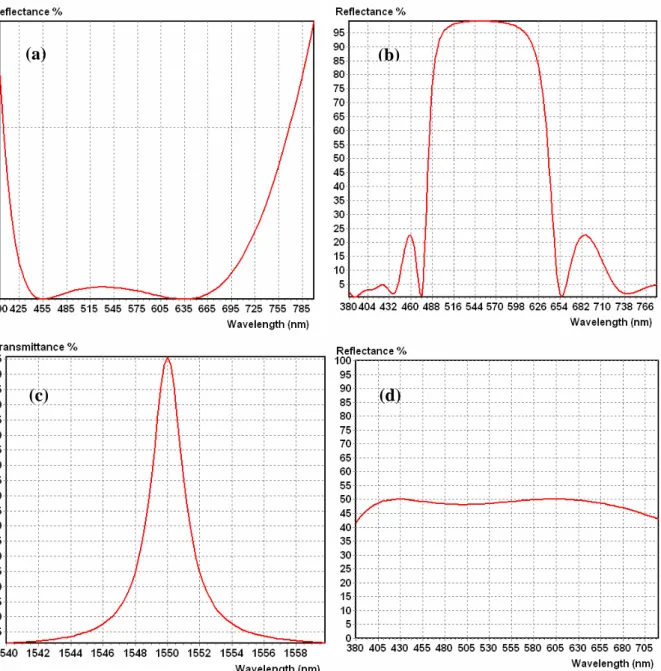
Single wavelength reflectometry has been used for a long time for monitoring optical layer deposition [6]. This method is very suitable for the control of QWOT multilayer depositions, since the ideal optical thickness of each layer corresponds to an interferometric maximum or minimum at the control wavelength. The technique can be used in either reflectance or transmission mode. Figure 1.8 shows the reflectance profile of a standard three layer antireflection coating on glass for the visible range.
This method can also be used for arbitrary thicknesses by changing the control wavelength for each layer, on the condition of having thicknesses higher than a QWOT of the deposited material for the lowest wavelength allowed by the apparatus.
F A m d ρ ∆ = ∆
Figure 1.8. Reflectance evolution at 530 nm, for monitoring an M2HL visible ARC.
A newer control method, based on broadband spectroscopic reflectometry, is currently widely applied. It uses an array of photodiodes to do the acquisition at different wavelengths, which permits fast spectroscopic measurements on the order of a few seconds. It consists of the following steps [17-20] :
• Estimating the current layer’s deposition time, taking into account the thickness accuracy. • Stopping the deposition a few percent before the estimated time.
• Taking a wideband measurement of the reflectance or transmission of the deposited layer and calculating the necessary thickness correction.
• Repeating the procedure until reaching the required thickness.
This method is more suitable with deposition systems allowing homogeneous and dense materials, such as magnetron sputtering [21]. It is less accurate with e-beam systems, where porosity needs to be taken into consideration [19].
Kinetic ellipsometry for deposition control will be discussed in Chapters 4 and 5. The advantage of this technique lies in its suitability for all deposition techniques and its fast acquisition rate of less than one second.
References
[1] G.M. Wells (Chairman), The Application of Metallic Fluoride Reflection Reduction Films to Optical Elements, Published at Frankford Arsenal, (October 1943).
[2] J.A. Dobrowolski, Optical properties of films and coatings, in Handbook of Optics,
Vol. I, (M. Bass, E. W. van Stryland, D. R. Williams, and W. L. Wolfe, editors), McGraw-Hill, (1995).
[3] L. Martinu, Plasma deposition of optical films and coatings: A review, Journal of
Vacuum Science and Technology A, Vol.18 (6), pp. 2619-2645, (2000).
[4] J.A. Dobrowolski, D. Poitras, P. Ma, H. Vakil and M. Acree, Toward perfect antireflection coatings: numerical investigation, Applied Optics, Vol. 41(16),
pp. 3075-3083, (2002).
[5] S. Furman, A.V.Tikhonravov, Basics of optics of multilayer systems, Editions
Frontières, Gif-sur-Yvette, (1992).
[6] H.A. Macleod, Thin Film Optical Filters, 2nd edition, Macmillan, New York, (1986). [7] A. Thelen, Design of Optical interference Coatings, McGraw-Hill, (1988).
[8] F. Abelès, Annales de Physique 5, pp. 596-640, 706-782, (1950).
[9] R. Petit, Ondes Électromagnétiques en radioélectricité et en optique, Masson, (1988).
[10] A. Macleod, Oblique incidence rules, SVC Winter Bulletin, pp. 22-28, (Feb. 2006).
[11] M.A. Lieberman, A.J. Lichtenberg, Principles of plasma discharges and materials processing, 2nd edition, John Wiley & Sons, (2005).
[12] D.M. Dobkin, M.K. Zuraw, D. M. Dobkin, Principles of chemical vapor deposition,
Kluwer Academic Publishers, (2003).
[13] M. Ohring, Materials science of thin films, deposition and structure, 2nd edition, Academic Press, (2002).
[14] F.F. Chen, J.P. Chang, Lecture notes on principles of plasma processing, University of
California, Los Angeles, (2002).
[15] M. Moisan, J. Pelletier, Physique des plasmas collisionnels: Application aux décharges hautes fréquences, EDP Sciences, (2006).
[16] C. Buzea, K. Robbie, State of the art in thin film thickness and deposition rate monitoring sensors, Reports on Progress in Physics, Vol. 68(2), pp. 385-409, (2005).
[17] B.T. Sullivan, J.A. Dobrowolski, G. Clarke, T. Akiyama, N. Osborne, M. Ranger, L. Howe, A. Matsumoto, Y. Song and K. Kikuchi, Manufacture of complex optical multilayer filters using an automated deposition system, Vacuum, Vol. 51(4),
pp.647-654, (1992).
[18] B.T. Sullivan, G. A. Clarke, T. Akiyama, N. Osborne, M. Ranger, J.A. Dobrowolski, L. Howe, A. Matsumoto, Yizhou Song and Kazuo Kikuchi, High-rate automated deposition system for the manufacture of complex multilayer coatings, Applied Optics,
Vol. 39(1), pp.157-167, (2000).
[19] B.T. Sullivan, J.A. Dobrowolski, Deposition error compensation for optical multilayer coatings: I. Theoretical description, Applied Optics, Vol. 31(19), pp.3821-2835,
(1992)
[20] B.T. Sullivan, J.A. Dobrowolski, Deposition error compensation for optical multilayer coatings. II. Experimental results-sputtering system, Applied Optics, Vol. 32(13), pp.
2351-2360, (1993).
[21] J.A. Dobrowolski, James R. Pekelsky, R. Pelletier, M. Ranger, B.T. Sullivan, A.J. Waldorf, Practical magnetron sputtering system for the deposition of optical multilayer coatings, Applied Optics, Vol. 31(19), pp. 3784-3789 (1992).
Chapter 2
H
igh Density Plasma Sources
M
icrowave excited plasmas are acquiring more and more importance as they can generate high-density plasmas over a large pressure range [1, 2]. In this study, the microwave excited plasma in which we are specifically interested is the Electron Cyclotron Resonance (ECR) discharge that has been adapted from fusion technologies to surface treatment processes such as cleaning, deposition and etching.ECR plasma sources, together with inductively (also called transformer) coupled and helicon sources, form the pillars on which high density plasma (HDP) PECVD is built. High density plasmas offer several characteristic features, including low pressure operation, large and highly controllable ion fluxes and heterogeneous reaction modes. Several processes benefit from these features, such as etching, plasma immersion ion implantation and surface cleaning, to name a few.
This chapter will begin by giving a brief overview of laboratory plasmas and their properties in Section 2.1, before discussing microwave plasmas and ECR discharges in Section 2.2. Section 2.3 will then focus on the different ECR reactors currently in use. This will serve to explain the choice of a matrix distributed (MD)ECR-PECVD system and provide the necessary background for Chapter 3, where the MDECR-PECVD reactor developped during this study is presented.
2.1. Plasma and Plasma Properties
A plasma can be defined as a gas containing charged and neutral species [3, 4] showing collective behavior. It consists of electrons, positive ions, negative ions, atoms, radicals, molecules and sometimes, in the case of dusty plasmas, atomic clusters with a negative charge. On average plasmas are electrically neutral, since any charge imbalance would create electric fields that would tend to move the charges to eliminate the imbalance. As a result, the combined density of electrons and negative ions will be equal to that of positively charged ions in any given volume of plasma. This property of plasmas is called quasi-neutrality.
Plasmas have two important characteristics making them ideal for thin film processing. Firstly, they are sources of chemically active species, radicals and ions that result from the collision of neutral background gases with electrons which are sufficiently energetic to break their chemical bonds. Substrate surface reactions can thus take place at much lower temperatures than in thermal processing. Secondly, low-pressure plasmas offer the added advantage of a non-collisional sheath, ensuring that the energy of the ions striking the surface can be accurately controlled within a broad range. Energetic ions play a synergetic role in deposition and etching processes and a determining role in sputtering processes.
Plasmas can be described by several important parameters [4-7]. These include:
• The plasma density ne, which is the concentration of charged species of the same sign. • The plasma temperature Te, which is the electron temperature measured in eV.
• The degree of ionization, which is the fraction of the original neutral species (atoms and molecules) that have been ionized. Plasmas with a degree of ionization much less than unity are referred to as weakly ionized plasmas.
• Other plasma parameters, such as collision frequency, Debye length and plasma frequency, will be discussed later in this chapter.
In order to have ionization, a constant source of energy is required. The loss of both ions and electrons due to recombination and diffusion and/or convection to the walls must be balanced by the rate of ionization. All technological plasmas are initiated and sustained by electric fields, produced by either direct-current (DC) or alternating-current (AC) power supplies. Typical AC frequencies of excitation are 100 kHz in the low frequency range, 13.56 MHz and its harmonics in the RF range and most commonly 2.45 GHz in the microwave region. These plasmas are sometimes correspondingly referred to as electric, gaseous or glow discharges.
2.2. Microwave Discharges and the ECR Effect
2.2.1. The Motion of a Charged Particle in an Electromagnetic Wave
The theoretical study of microwave plasmas is done by solving the equation of motion for an electron in an electromagnetic harmonic field [1, 2, 8]
(2.1)
It suggests a fluid model of electrons in motion with mean velocity V of the particle and several hypotheses and simplifications:
• The magnetic force of equation (2.2) is negligible compared to the electric force.
(2.2)
• No motion of ions, which are heavy compared to the electrons.
• The collision frequency between an electron and heavy particles is given by ν. ) exp( ) exp( t j H t j E ω ω c V eE FM ≈ ×
The resulting equation of motion is then
(2.3)
The first term of the right hand side of the equation (2.3) refers to the electric force, and the second term to the friction force. The mean velocity is thus given by
(2.4)
The solution results in several characteristic definitions, such as the root mean square value of electron displacement:
(2.5)
As this value is small compared to the reactor’s dimensions, collisions with the walls can be neglected. The electron-plasma angular frequency is given as:
(2.6)
This value depends only on the electron density. It is used to define the plasma density and identification of the different plasma zone types by comparing it with the electromagnetic field frequency [6].
The Debye length is given by
(2.7)
With the electron temperature Te in Volts. The Debye length depends on the electron temperature and density. It represents the length over which a significant variation of charge density can only be observed, and is used as a characteristic dimension of the plasma and the sheath. v V m t eE dt dV me =− ( )− e ⋅ ω j v m eE e
V
=
−
+1 2 / 1 2 2 ) (ν ω ω +=
e rms m eE rmsr
2 / 1 0 2)
/
(
ε
ω
pe=
ne
m
e ) ( 743 2 1 cm n T m T k e e pe e e B D ⎟⎟ ≈ ⎠ ⎞ ⎜⎜ ⎝ ⎛ = ω λFor ECR plasmas the study is very similar, with the exception of two points [1,2]:
• The collision frequency is much lower due to the very low pressure (in the mTorr range) consequently the MFP is much greater and the electrons reach ionization energy with fewer or no elastic collisions.
• We can only neglect the magnetic field linked to the EM wave. The static magnetic field created by the permanent magnets or the magnetic coils cannot be neglected. It creates the cyclotronic motion of the electrons, which will be discussed in the following section.
2.2.2. The Larmor Radius and the ECR Effect
The trajectory of a charged particle in a static magnetic field is determined by the Laplace force[4] :
(2.8)
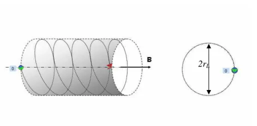
Under a constant magnetic field and in the absence of electric force it will follow a helicoidal trajectory with a constant radius. The Larmor radius is the characteristic of this cyclotronic motion which is the gyration of the charged particle in the magnetic field. In ECR, it is specifically used to describe the motion of electrons.
For an electron in a constant magnetic field, the Larmor radius is given by the formula
(2.9)
where me is the electron mass, T its kinetic energy, Ve its velocity, e the charge of the electron and B the magnetic field strength, as shown in Figure 2.1. The subsequent Larmor angular frequency will then be
) (V B q F = × eB V m eB T m r e e e L = = 2 e L m eB = ω
(2.10)
Figure 2.1. Motion of an electron and Larmor radius in a constant magnetic field.
Figure 2.2. Trajectory of an electron under the ECR effect and the resulting increase in the Larmor radius.
When applying microwaves, the alternating electric field (§ 2.2.1) will contribute to this motion. As can be seen in Figure 2.2, resonance will exist when the microwave frequency is equal to the Larmor frequency:
(2.10) L
MW ω
ω ≈
This signifies that the motion of the electron in the field created by the magnets is in harmony with the electric field generated by the microwaves. In the absence of collisions, the electric field constantly increases the electron velocity, and consequently its kinetic energya beyond the ionization threshold required for ionization and the creation of discharges [8, 9]. For a standard microwave power supply operating at 2.45 GHz, ECR will occur in the regions where the magnetic field component perpendicular to the plane of oscillation of the electric field vector is equal to 875 Gaussb.
Operating at low pressure is an important condition to ensure a sustained ECR effect. Pressures below 10 mTorr are normally used. Higher pressures will increase the collision frequency, which in turn will result in a transition to a collisional microwave plasma [9].
2.3. Low Pressure Microwave Reactors
ECR plasmas have distinct features due to the high ionization and gas dissociation levels at low pressures [9]. The plasma and deposition processes under such conditions depend on several parameters [10], such as the pressure, microwave power, substrate temperature and reactant gas flows. Additionally, the energy and flux of impinging ions depend on these parameters and may additionally be controlled by RF biasingc. To apply ECR technology towards thin film fabrication, several different designs of ECR reactors have been developed[11], including divergent ECR, microwave plasma disk reactors, distributed ECR, integrated ECR and multi-dipolar (or matrix distributed) ECR reactors.
a
Figure 2.2 illustrates this phenomenon. When the radius increases while the gyration frequency is constant, the electron’s velocity should increase to make a complete turn for each period.
b GHz B Tesla G m eB e 875 08753 . 0 45 . 2 2 × ⇒ ≈ ≈ = π . c
2.3.1. Divergent ECR
Divergent ECR PECVD systems, also referred to as NTT reactorsa, are considered to be the most typical ECR reactors. The microwaves, traveling through a rectangular or circular waveguide, are introduced into the vacuum chamber through a dielectric window [11]. One or several magnetic coils wound around the reactor are used to form a magnetic field with a specific strength and profile. The reactor volume may have from one to several ECR regions. The magnetic field profile along the chamber axis can be adjusted in order to localize the ECR region of the plasma where it is necessary. Figure 2.3 shows an example of such a reactor, taken from the literature [12].
The main disadvantage of these reactors is the radial non-uniformity of the field and thus scaling up beyond 50 cm proves difficult. The deposition of conductive materials such as a-Si on the microwave window may cause the reflection of microwaves and the gradual attenuation of the electric field beyond the dielectric window, while etching can also damage the window [12]. These systems are however the only commercially produced reactors for VLSI technology and used mainly for metal etch applications.
Figure 2.3. Divergent ECR system with resonance locations as modeled in [12].
a
2.3.2. Microwave Plasma Disk Reactors
The microwave plasma disk reactor (MPDR) was developed by Jes Asmussen of Michigan State University [13-17]. It combines multipolar magnetic confinement with a resonant cavity and internal tuning. The microwave mode can be chosen precisely by using such an arrangement, normally excited by a probe antenna. The cavity can be matched over a broad pressure range, from below one mtorr to over 300 torr. Operating as a resonant cavity, an applicator can induce a high strength tangential field against the top of the quartz discharge chamber without reflecting the power from the applicator. Very high powers can thus be coupled into the plasma by an evanescent electric field.
Figure 2.4 shows a commercial MPDR, from which it can be seen that the quartz discharge chamber is a serious drawback, as are the permanent magnets on the chamber’s border. Similar to divergent ECR systems, this window is sensitive to damage from etching gases and deposition of conductive layers. Additionally, the rapidly decreasing magnetic field of the permanent magnets will not only expand the ECR zone away from the wafer surface, but will also present a serious problem for scaling up the system due to the increasing radial non-uniformity [17].
2.3.3. Distributed ECR
The configuration of the magnets and antennas on the periphery of Distributed ECR reactors, an example of which is presented in Figure 2.5, is suitable for producing a uniform deposition on a large area between the antennas by diffusion of ionized species [18]. A benefit of these reactors is the ease with which the reactor may be scaled up by simply adding extra antennas and magnets, thus enlarging the plasma. The magnets contribute simultaneously to the ECR effect and to the plasma confinement. However, even if the plasma is uniform in the plane perpendicular to the antennas, it is not uniform along the axis, parallel to the antennas, because of attenuation of the microwaves along the applicators. Moreover, with increase of the radius of reactor, plasma density in the center tends to drop.
Figure 2.5. Divergent ECR plasma with magnet and antenna positions.
To overcome this problem, a configuration with standing waves with constant quasi-amplitude has been suggested [18]. A considerable reflection on the end of the antennas is consequently needed, therefore a high power supply and the low absorption of microwaves are necessary, which is technically difficult to realize. Moreover, each of the magnet sets and antenna sets need a cooling system. Integrated Distributed ECR, which is discussed next, seems to be a solution for some of these problems.
2.3.4. Integrated Distributed ECR
IDECR reactors allow a single cooling system for all the antennas and perfect proximity of the antennas and the magnets. Figure 2.6 shows the reactor Plasface, in the PICM Laboratory. The configuration consists of microwave antennas enveloping long magnets of SmCo5 with alternating polarities facing the substrate [19].
Figure 2.6. The IDECR reactor Plasface [19].
Enlargement of the deposition surface consists of increasing the number and the length of the antennas. The problem of microwave propagation and high interaction between the antennas, causing instability are still limiting factors in the scale-up of IDECR reactors. In addition, the lengthening of magnets is not a simple problem to solve.