Superconducting properties of natural and artificial grain boundaries in
bulk melt-textured YBCO
Ph. Vanderbemden a,b, A.D. Bradley b, R.A. Doyle b, W. Lo b, D.M. Astill b, D.A. Cardwell b, A.M. Campbell b
a SUPRAS, Montefiore Electricity Institute B28, University of Liège, Sart-Tilman, B-4000 Liège, Belgium bIRC in Superconductivity, University of Cambridge, Madingley Road, Cambridge CB3 0HE, UK
Abstract: A range of experimental techniques have been used to characterize melt-processed YBa2Cu3O7-δ
samples containing single-grain boundaries. Both natural high-angle boundaries, which sometimes appear during the grain growth process, and artificial low-angle boundaries, obtained by joining two single domains, have been investigated. Electrical resistivity, current-voltage characteristics, magnetic moment measurements and Hall probe mapping techniques have been employed to investigate the boundaries. Results are compared with the properties of single domain material (i.e., containing no grain boundary) for which Tc ≈ 89 K and Jc||ab (77 K, 1 T) > 104 A/cm2. Resistance measurements across all the grain boundaries show a stronger dependence on current and magnetic field than that measured within the grains and exhibit a pronounced resistive 'tail'. The I-V curves obtained for the high-angle natural grain boundary are sharp and differ from the rounded I-V curves which are characteristic of single-grains. Field mapping measurements used to evaluate the critical current anisotropy are in agreement with magnetisation measurements. The limitations of this technique for investigating boundaries are discussed. It was found that current anisotropy can conceal a weak link between two grains, leading to a false indication of single-grain behaviour. Artificially engineered boundaries are shown to have significant potential for applications in high fields at 77 K.
Keywords: High-angle boundaries; Low-angle boundaries; I-V curves
1. Introduction
Quasi single-crystalline monolithic melt-textured YBa2Cu3O7 (YBCO) has been shown to be able to trap significant magnetic inductions ( > 2 T) at liquid nitrogen temperature [1]. As a result these materials have clear potential for permanent magnet engineering applications such as superconducting motors, magnetic bearings and flywheels [2]. The maximum induction which can be achieved in bulk superconductors is determined by the product of the critical current and the radius over which it flows. It is, therefore, limited by any weak links which connect regions of otherwise strongly superconducting material, and also by solid state chemical considerations which make it very time consuming to grow samples larger than 3-5 cm in diameter.
The microstructure of melt-processed YBCO monoliths [3] generally consists of a pseudo-crystalline YBa2Cu3O7 (Y-123) matrix containing secondary phases, mostly Y2BaCuO5 (Y-211), and other defects such as cracks, twins and stacking faults. These defects can provide strong pinning centers which are essential for high Jc material although they frequently also restrict the uniform flow of current within the specimen. The Y-123 matrix itself is composed, characteristically, of large parallel platelets with parallel c-axes but which may be rotated in the ab-plane.
Regions of large single domains in melt-processed YBCO are known to be separated by domain (or grain) boundaries. In general, applying an external magnetic field to a ceramic superconductor induces intragranular shielding currents which circulate within the grains and intergranular currents which flow through grain boundaries. However, the undesirable natural grain boundaries which may form during growth of the YBCO pellet often have high-angle misorientation ( > 10°). In this case the intergranular critical current density is usually considerably less that of the grain and, in addition, decreases by several orders of magnitude in the presence of small magnetic fields ( ≈ 10 mT) [4]. The average trapped magnetic induction generated by a multi-grain pellet is therefore due mainly to intragranular currents.
On the other hand, although large YBCO single domains up to 7 cm diameter have been successfully synthesised by a top seeding technique [5], it is known that the intragranular Jc degrades with the increasing distance from
the seed [3]. On this basis it would appear to be technologically important to produce larger samples by joining single domains. This requires the creation of artificial low-angle grain boundaries to ensure good connectivity between two adjacent single domains, i.e., with a high intergranular critical current density. The processing of
samples joined in this way which exhibit good transport carrying properties is a formidable challenge.
Understanding the transport current and magnetic behaviour of both natural (high-angle) and artificial (virtually zero-angle) grain boundaries necessitates reliable characterization. The weak-link behaviour of grain boundaries has been studied extensively since the discovery of high-Tc superconductors. Systematic investigations, however, have been reported mainly for artificially induced grain boundaries formed by thin films grown on bicrystal substrates [6] and intergrown bicrystals [7-9]. It has also been shown that the use of a multiple seeding growth technique can provide large and clean boundaries of general tilt and twist misorientation [6].
Electrical characterization in most of the studies performed to date involves measuring the transport critical current as a function of applied magnetic field and results suggest generally that the Jc(B) behaviour is strongly
dependent on the misorientation angle. A common feature of high-angle intergranular Jcs is their strong field
dependence, whereas no significant weak link effects are usually observed for misorientations less than 5°. This was confirmed by recent magneto-optical studies performed by Uspenskaya et al. [10]. It should also be emphasized that interpretation of I-V characteristics of grain boundaries requires great care since they may be sensitive to self-field effects and to inhomogeneity of current transfer between grains which often makes determination of critical current density difficult [7].
Another possible approach for evaluating the behaviour of grain boundaries in YBCO pellets is to measure the trapped flux by scanning a miniature Hall probe over the top surface of the sample [11-15]. Such measurement techniques are increasingly popular since they are non-destructive and may be applied to large samples. In some cases, the flux profile can reveal a granular microstructure and show the presence of detrimental barriers which inhibit the flow of superconducting current [11,12]. However, as will be shown here, this technique needs to be applied with considerable caution when evaluating the properties of grain boundaries in large samples.
The aim of the present work is to investigate the properties of grain boundaries in melt-processed YBCO with various measurement techniques including electrical resistivity, I-V curves, Hall probe mapping and magnetization. By comparing the properties of grain boundaries with those of single-grains, we are able to describe several important features characteristic of the boundaries.
2. Experimental techniques
2.1. Synthesis processes 2.1.1. Melt-processed materials
The precursor bodies used for melt-processing were prepared by uniaxial pressing and sintering a powder containing YBa2Cu3O7-δ + 0.3 Y2BaCuO5 and 0.1 wt.% of Pt [16]. A SmBa2Cu3O7-δ seed was placed on top of the sintered precursor body, which was then heated to 1025°C in a thermal gradient box furnace [17] to peritectically decompose the Y-123 phase. The sample was then crystallized by slow cooling in air at 0.3°C/h between 1000°C and 900°C [3]. YBCO single-grains up to 3 cm diameter can be fabricated routinely by this technique.
2.1.2. Artificial boundaries
Large YBCO grains were selected from melt-processed YBCO bodies prior to the joining process and cleaved or cut along their crystallographic ab-planes. These planes were used as a reference for further processing of the grains, such as cutting and polishing. Grains of selected orientations were stacked in a furnace at room temperature with their smooth surfaces in contact and a static pressure of 0.5 MPa applied to the top of the stack. These grains were then joined by heating the loaded arrangement to a temperature between 920°C and 980°C. The detailed mechanism whereby the joining takes place is as follows. Between 920°C and 980°C, Ba-Cu-O, trapped in the platelet boundaries during the original fabrication of the samples becomes liquid. Large numbers of platelet boundaries (always in the ab-plane) invariably intersect the boundary to be joined, at an angle which depends on the choice of angle of the final boundary. Even for artificially prepared 'c-axis' boundaries, which are in principle parallel to the platelet boundaries, preparation of the faces to be joined invariably exposes a small number of platelet boundaries to the surface because of their small thickness and the difficulty of polishing the surface perfectly flat and smooth. Once the Ba-Cu-O phase becomes liquid, it migrates into the surface to be joined, no doubt assisted by surface tension effects. Once there, it dissolves 123 phase which later recrystallises during cooling, driving the impurity phase out of the boundary and forming a robust join as the sample solidifies. Solid state diffusion (the sample is rather close to the melting temperature of 123) under the action of the
imposed pressure may also assist in formation of a good boundary. As will be shown below, although we do not yet understand the detailed mechanisms of intergrowth across the interface, it is nonetheless clearly able to produce boundaries which do not display the usual characteristic features of defected links.
2.2. Transport measurements
Bar-shaped samples of typical size 2 × 0.3 × 0.3 mm3 intended for transport measurements were cut from the initial melt-processed sample using a wire saw. Each specimen contained either a single-grain or two adjacent grains with the boundary approximately perpendicular to the length of the bar. The grain boundary structure could be observed in the latter on all four faces of the specimen after polishing. Ohmic contacts were made by initially depositing Ag onto the sample by thermal evaporation. Thin gold wires (25 µm diameter) were attached to the contacts with silver epoxy and annealed in O2 at 420°C for 5 min. In samples containing grain boundaries, voltage contacts were placed both within the grains and across the well-defined grain boundary (see Fig. 1). In practice YBCO monoliths are prone to fracture along the ab -planes during cutting due primarily to the presence of the platelet boundaries, even when low cutting rates are used (10 µm/h). For this reason, the determination of the c-axis resistivity of the single-grain had to be performed on a flat sample (size 1 × 1 × 0.3 mm3) with the c-axis parallel to the shorter dimension of the specimen. In this case the current and voltage electrodes were attached using silver epoxy paste in the configuration depicted in Fig. 1b. By assuming a priori that ρc>> ρab, both the large rectangular upper and the lower faces are expected to be effectively equipotential
with the current inside the specimen flowing almost uniformly over the entire specimen cross-section. This configuration is thus a reasonable approximation to the classical four-point technique provided that the resistivity anisotropy is sufficiently high. The anisotropy ratio measured in this single-grain sample was found to exceed 80 (see Section 2.3). However, because a small component of in-plane resistivity cannot be excluded, this value is only a lower bound for the true anisotropy ratio.
Fig. 1: Schematic diagram of experimental arrangements used for transport measurements on samples having
ab-planes (a) or c-axis (b) current flow and samples containing one grain boundary (c).
Electrical resistance as a function of temperature was measured using the four-point technique described above. In addition, the potential differences across the grain and the grain boundary were recorded simultaneously. A constant alternating current (ƒ= 73 Hz) was injected through the sample and the resulting voltages amplified using a low-noise transformer prior to measurement by an EG&G 5210 Lock-In Amplifier. This method eliminates spurious thermoelectric effects and enables sub-nanovolt resolution to be achieved. In addition, I-V curves were measured with a programmable Keithley 220 DC current source and a Keithley 182 nanovoltmeter. A conventional iron-cored electro-magnet was used to apply low magnetic fields (B < 0.3 T), whereas higher magnetic fields up to 7 T were generated with an Oxford Instruments superconducting magnet.
2.3. Magnetic measurements
A cubic sample geometry was selected for the magnetic measurements (side length 2 mm) with two faces parallel to the ab planes of the single-domain. In this geometry, the demagnetization factor D is strictly the same
(approximately 1/3) for H||ab and H||c. This allows us to attribute any flux penetration anisotropy to the material microstructure and not to geometric effects.
A commercial Quantum Design SQUID was used for the measurement of DC magnetic moment loops. The applied magnetic field was swept from - 5 T to + 5 T and a small scan length (5 cm) selected to ensure reasonable field uniformity. The remnant field of the superconducting magnet was eliminated before each measuring sequence by the standard practice of applying a succession of decreasing fields in alternate directions. The spatial distribution of trapped magnetic induction was measured by scanning a miniature Hall probe fixed to a motor-driven xyz micro-positioning stage over the sample surface. The specimen was initially cooled to 77 K in an applied magnetic field of 0.5 T (Field Cooled). This external field was then removed and the Hall probe moved across the top surface of the specimen parallel to both x and y with a step size of 0.1 mm in each direction. The active area of the Hall probe, sensitive to the component of the local induction parallel to the applied field (i.e., perpendicular to the surface), was 0.1 × 0.1 mm2. The probe is nominally in contact with the sample. In practice, it is separated from it by a layer of varnish to protect the surface of the Hall probe.
We estimate the thickness of this layer to be about 0.1 mm. This value is larger than the penetration depth so that some 'smearing' of the measured signal is expected.
3. Characterization of the single domains
3.1. Transport measurements
Fig. 2 shows the temperature dependence of the electrical resistivities ρab and ρc for a single-grain with an
injection current (1 mA) parallel and perpendicular to the ab-planes of the sample respectively. It can be seen that both transitions are very sharp (∆T< 1 K). The critical temperatures determined from the ρab(T) and ρc(T)
plots are 88 K and 89.5 K, respectively; the small difference can be attributed to different oxygenation levels within the samples. It can also be seen that the ab-plane resistivity displays a quasi-linear metallic behaviour in the normal-state. The residual resistivity obtained by extrapolating the normal-state resistivity down to T = 0 is slightly negative and this characteristic has also been reported for Y-123 single crystals [18]. It is supported by the fact that ρab(T) is weakly non-linear above Tc. The c-axis resistivity is much larger than ρab and weakly
metallic in nature. The anisotropy ratio ρc/ρab measured at room temperature is 80, which is well within the range
that would be expected for a single crystal (30 to 100) [18]. This would suggest, therefore, that platelet boundaries and microcracks do not significantly impede the flow of current parallel to the YBCO c-axis.
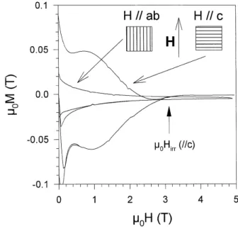
Fig. 3: Magnetization as a function of internal field for single-grain samples with H\\c and H\\ab at a
temperature of 77 K.
3.2. Magnetic measurements
Fig. 3 shows M(H) curves measured on a cubic single-grain sample at T= 77 K for H||c and H||ab. The applied field has been corrected for the demagnetization factor in this data by using the formula Hcorr = Happ - DM, where Hcorr and Happ represent the corrected and the applied magnetic field, respectively. The well-known 'anomalous-peak' or 'fishtail' is clearly apparent at µ0H ≈ 0.9 T for H||c. This effect has been reported for both Y-123 single
crystals [19] and melt-processed YBCO [20]. It has been attributed variously to oxygen deficient regions having lower Tc and Hc2 and acting as field-induced pinning centres [21] or to dynamic effects [22]. This peak is absent
when H||ab (Fig. 3), which is to be expected since it is related to currents circulating in the ab-planes [19]. The irreversibility field, Hirr, can be determined from the point where the upper and the lower branches of the
M-H loop converge. The value of µ0Hirr for H||c is 3.1 T and greater than 5 T (the maximum field which could be applied) for H||ab.
An anisotropy in Hirr has also been reported for single crystals [23] and is consistent with the much larger Hc2 value for H||ab compared with H||c.
The intragranular critical current derived from M(H) measurements using the Bean model [24] is plotted in Fig. 4. The value of the ratio Jcab/Jcc (inset in Fig. 4) measured at 77 K is close to 3 for small magnetic fields, in
agreement with results obtained in Ref. [25] and with recent magneto-optical measurements [10] performed on large grain melt-processed YBCO.
Although we have assumed, in the above calculation of Jc, that screening currents flow right across the sample, it
is important to know if M(H) loops measured on single domains can give any information about the length scale over which shielding currents, Is, really flow. To investigate this, magnetization loops were measured at 80 K on a rectangular single-grain specimen (4x2x2 mm3). This sample was then cleaved in two identical cubes (2x2x2 mm3), and M(H) measurements repeated on the two cubes positioned side by side and attached with insulating GE varnish. Sample geometries and results are presented in Fig. 5. The small decrease of the total sample volume caused during cutting has been taken into account during calculation of the magnetization from the measured magnetic moment in this data.
Fig. 4: Critical current densities extracted from the magnetization loops shown in Fig. 3. Inset: field variation of
the ratio Jcab/Jcc at 77 K.
Fig. 5: Comparison of the magnetization as a function of internal field measured for the original single-grain
(SG) sample and the split double-grain (DG) sample at 77 K.
The induced currents circulate parallel to the cutting plane when the applied magnetic field is directed parallel to the c-direction of the lattice and hence, should not be influenced by the cutting and rejoining process. This is illustrated in Fig. 5 which shows that the M(H) loops for the original and the GE varnish joined samples coincide. When the applied magnetic field is directed parallel to the insulating joint, however, the situation is
more complex. Accordingly, we calculate the expected difference in moment after cleaving of the crystal. We assume a Bean model and that currents loops flow over a length scale comparable to the sample size. The anisotropy ratio of critical currents is denoted by r = Jcab/J
cc. Generally speaking, for a rectangular sample with side lengths x and y (x ≤ y), thickness t and for an applied field H\\ y\\ab-plane, the magnetic moment m is given by
In our case, the starting single-grain (SG) dimensions are t = s, x = s, y = 2s. As a consequence, we expect the magnetic moment m to be given by
while for the cleaved and glued pair (double-grain DG) it should be given by
The anisotropy ratio r characteristic of our single-grain material is found to be close to 3 (cf. insert in Fig. 4). For this value of anisotropy, both calculated magnetic moments (for the single and cleaved samples, respectively) have a very close value. This is in fairly good agreement with the measured difference which lies between 10% and 20% (depending on the applied magnetic field). Note that even if an isotropic current flow was assumed (Jcab = Jcc, leading to r = 1), the calculated difference would be 25% only. On the other hand, if the specimen was granular and the length scale for current flow was much smaller than the size of the single-grains, both magnetic moments should have exactly the same value. This means that the magnetization is only weakly sensitive to the current length scale, particularly if the critical current anisotropy ratio is taken into account. In addition, it should be emphasized that the above calculations are at best semi-quantitative, since they neglect corner effects. Therefore, although magnetization measurements are clearly not the most sensitive method for determining the current length scale, the significant difference between magnetization loops in Fig. 5 when H||ab gives us indirect but reasonable proof that this current length scale is macroscopic rather than microscopic. This is also consistent with independent evidence from the transport measurements (Fig. 2), that supercurrents indeed flow right across the sample and self-consistently supports our assumptions in the calculation of Jc in Fig. 4.
It can be concluded from the above results that the single-grain properties are characteristic of good-quality melt-processed YBCO material and that defects in the microstructure do not influence significantly the uniform current flow. Having established the properties of the bulk YBCO material, the effect of domain boundaries will now be discussed.
4. Characterization of a natural high-angle boundary
The high-angle naturally occurring grain boundary is illustrated schematically in Fig. 6 together with the resistance as a function of temperature measured within the single-grain (G) and across the grain boundary (B) for currents from 3 mA to 30 mA. The latter value corresponds to a current density of 15 A/cm2. The resistive transition of the grain is observed to be sharp without any intermediate step. The grain boundary R(T) curve, on the other hand, decreases sharply at T= Tc before levelling off to form a 'foot-like' structure towards the bottom
of the transition. The initial decrease is caused by the superconducting transition of the grains whereas the broader feature can be attributed to the boundary. The tail shape is very similar to the thermally activated phase slippage (TAPS) observed in over-damped Josephson junctions [26,27]. Both grains become superconducting at
T ≈ Tc but the Josephson coupling energy EJ is smaller than the thermal energy kT. The phase coherence between the order parameter of the two neighbouring superconductors is then affected by thermal fluctuations and can slip by 2π, which results in a non-zero time-averaged voltage [26-28]. This corresponds in a finite resistance. EJ increases as the temperature decreases further and until it exceeds kT. The boundary is then able to carry a supercurrent and its resistance vanishes. It is also worth noting that the resistive tail broadens significantly with a small increase of injection current (cf. Fig. 6) whereas the grain transition remains largely unaffected by this parameter. The above results indicate clearly that these measurements characterise the grain boundary.
Fig. 6: Schematic diagram of a naturally occurring grain boundary studied in this paper and comparison of the
resistance measured across this high-angle grain boundary (B) and within an YBCO grain (G).
Fig. 7: I- V curves measured across the grain boundary at T = 77 K.
The current-voltage characteristics across the natural boundary measured at 77 K and for different applied magnetic fields are shown in Fig. 7. The sharp onset of voltage at Ic and the strong dependence on even very
small magnetic fields are again characteristic of Josephson-like boundaries. This behaviour differs from the more rounded I-V curve characteristic of a single-grain.
The latter two transport measurements (R-T and I-V) are particularly useful for elucidating features representative of the weakly-linked (high-angle) natural grain boundary, for which the intergranular current density measured at 77 K and zero-field was 2 A/cm2. This value is too low to enable intergranular currents to contribute significantly to the trapped induction of melt-processed YBCO, which underlines the importance of joining YBCO single-grains by fabricating artificial low-angle grain boundaries.
5. Characterization of artificial low-angle grain boundaries
Two kinds of low-angle artificial grain boundaries were investigated as shown schematically in Fig. 8. The c-axis of each grain in 'c-c-axis boundaries' is perpendicular to the boundary plane and hence parallel to the direction of current flow (Fig. 8a). On the other hand, the c-axis is parallel to the boundary plane in the case of the 'ab-plane boundaries' and current transfer occurs along the ab-'ab-planes (Fig. 8b).
5.1. Artificial c-axis grain boundaries
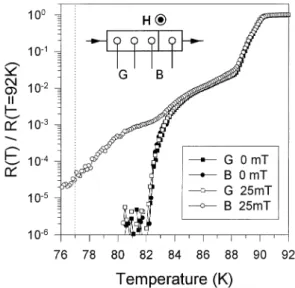
The electrical resistance of the artificial boundary was measured by electrodes placed within the grain (G) and across the boundary (B). An injection current of 1 mA was used in this measurement, corresponding to a current density of 0.4 A/cm2. The applied magnetic field was either 0 or 25 mT parallel to the boundary. The resulting
R(T) curves for the c-axis boundary, normalized at 92 K, are compared in Fig. 9. The grain transition (squares) is
seen to exhibit two steps, occurring at T ≈ 89 K and T ≈ 83 K. This double-step behaviour could be due to inhomogeneous oxygenation of the grains in this particular sample. In a zero applied field the grain and the boundary curves coincide. This is no longer true, however, when a 25 mT field is applied parallel to the boundary plane, in this case a significant broadening of the boundary transition occurs. This feature suggests a strong decrease of the intergranular c-axis critical current with increasing magnetic field. As a consequence, these measurements clearly show that the artificial c-axis boundary is incapable of sustaining a current density of 0.4 A/cm2 at T = 11 K and in a field of 25 mT.
Fig. 9: Comparison of the resistance measured within an YBCO grain and across an artificial c-axis grain
boundary.
Fig. 10: Distribution of magnetic induction on the surface of a sample containing an artificial c-axis grain
boundary. µ0Happ = 10 mT, T = 11 K.
The results of Hall probe mapping carried out close to the surface of the c-axis boundary are shown in Fig. 10. The sample edges and the boundary position are indicated in the diagram. Initially, the sample was cooled down to 77 K in zero applied field. A magnetic field of 10 mT was then applied and the field distribution within the sample measured with a miniature Hall probe. Note that this field is larger than both the first and the full penetration fields for this sample orientation. This is essential because at fields smaller than the first penetration field, the screening currents would always flow within λ of the surfaces. Consequently, currents flowing on adjacent surfaces would completely cancel within the spatial resolution of our Hall probe, making investigation of the boundary behaviour impossible. The field map obtained (Fig. 10) using the conditions described above shows a unique set of screening ellipses (constant field contours) centered in the middle of the sample. The figure thus suggests that the two neighbouring grains are connected by shielding currents flowing across the boundary. In what follows we shall show that this is not correct, and that this and other features in the Hall scan in Fig. 10 arise from the particular experimental conditions. Note that if we simply assume the shielding currents to be intergranular, and evaluate the corresponding critical current density using the Bean model [24], we find a value of 25 A/cm2 at 77 K and 10 mT. By assuming J
c ~ 1/B, this critical current density would be 10 A/cm2 at
25 mT, which is 25 times larger than the value measured by transport measurements (< 0.4 A/cm2). This discrepancy is less surprising, because of a number of other features in the field map (Fig. 10). Firstly, we are unable to clearly resolve the effects of the edges of the sample and indeed the flux profiles do not reflect the
samples aspect ratio. Further, while flux is expected to enter at the edges, the field is apparently larger at the corners than in these regions. Certainly, the finite spatial resolution and size of the Hall probe, as well as its distance from the surface of the specimen, are expected to smear out the sample response and are consistent with most of the coarse features described above. However, before we return to a discussion of the possible pitfalls of a Hall scan in this configuration, we first address other possible sources of the observed discrepancy. In fact, many reasons may account for the difference between the transport and magnetic Jc measurements:
(i) The presence of pores reduces the effective cross-section of the samples used for R(T) measurements and consequently underestimates the transport Jc. However, it is unlikely that this could account for a factor greater
than 2.
(ii) The use of a simple Bean model, which strictly holds only for an infinite cylinder or slab, can result in a miscalculation of the magnetic Jc. However, the sample is fully penetrated when µ0H = 10 mT and the induction B is very close to µ0H. Consequently, demagnetization effects under these conditions are negligible and the error
associated with the Bean model subsequently small.
(iii) The induction is mapped on the top surface of the specimen and not in the interior. Since B ≈ µ0H, however,
the induction within the sample is probably close to that at the surface.
(iv) Finally, intragranular currents flowing sufficiently close to the grain surface may effectively cancel at the grain boundary, due to the limited spatial Hall probe resolution and its finite distance from the sample surface. In order to further investigate hypothesis (iv), we conducted an 'experimental simulation' to elucidate what we really observe in Fig. 10 and how we might interpret this. A 'zero intergranular critical current' boundary was prepared artificially by gluing 2 identical single-grain cubes (2x2x2 mm3) together with insulating GE varnish. In this case, field shielding can only result from currents flowing separately in each cube and the resultant flux profile can be interpreted clearly. A Hall probe mapping of the flux trapped by this specimen was performed for 3 different grain orientations with respect to the boundary plane. In all configurations, the c-axis of both grains are parallel to each other and the magnetic field H used to magnetize the sample was always parallel to the boundary plane. Results of these measurements are summarized in Fig. 11.
The first notable feature is that all the trapped flux profiles are slightly asymmetric with respect to the joined face (located at x = 0). This is probably due to a slightly larger value of Jc for the right-hand grain than for the
left-hand grain and will not be considered further in the present study. When the common c-axis of the grains is perpendicular to the boundary (configuration 1), only one peak is apparent in the flux profile. This is the same situation as that in Fig. 10, and allows us to elucidate why we see a single peak even when the connectivity is poor, and discussed in more detail below. For a c-axis aligned parallel to the joined plane and H parallel to c (configuration 2), the induction profile displays a plateau with its centre at the position of the resulting grain boundary. Two smooth peaks centred over each cube clearly emerge when H is perpendicular to c (configuration 3).
The behaviour illustrated in Fig. 11 can be explained qualitatively by considering the critical current density anisotropy in these specimens. According to SQUID measurements carried out on the same single-grain cubes (Section 3.2), the ratio Jcab/J
cc lies between 3 and 4 at T = 77 K in the presence of small magnetic fields. Current loops flowing over the sample cross-section, and reflecting this anisotropy, are illustrated schematically in Fig. 11. In configuration 1, the portion of current sheet adjacent to the insulating junction is quite narrow. This suggests that currents flowing in two opposite directions in the vicinity of the central plane may effectively cancel each other within the resolution of the Hall probe and, in consequence, only one peak is visible in the trapped flux profile. Configuration 2 is characterized by two sets of quasi-square current loops which reflect the lack of asymmetry in the ab-planes. This is an intermediate case between configuration 1 discussed above and configuration 3 for which the current sheets parallel to the boundary are relatively broad. In this case, current cancellation in the vicinity of the junction is less significant and the trapped flux exhibits two peaks, as illustrated by the experimental data. This simple model, based on the anisotropy in Jc, is then able to explain the
Fig. 11: Distribution of trapped magnetic induction on the surface of two joined single-grain cubes and
schematic diagram illustrating anisotropy of current flow in each case.
In considering the maximum value of the trapped induction, it is clear that configuration 2 (H||c and Jc||ab) gives
the highest induction (Bmax = 13.5 mT).
Configurations 1 and 3, for which H||ab and Jc partially circulates along the c-axis, are characterized by Bmax =
3.2 mT and 3.5 mT, respectively. The value of the ratio Bmax(||ab):Bmax(||c) is found to be 4 which is in excellent
agreement with the anisotropy ratio determined by the hysteresis measurements (Section 3.2).
It may be concluded from this experiment that the flux profile measured on the top surface of two neighbouring grains having their c-axis perpendicular to the grain boundary may display a single peak, even if the grains are fully decoupled, i.e., even if the intergranular critical current density is zero. This observation suggests that Hall probe flux mapping at the top surface of an YBCO pellet is not always sensitive to the presence of weak links in the sample microstructure. Consequently, great care is required when interpreting flux profiles obtained by this measurement technique.
In the particular case of the artificial c-axis boundary, the shielding profile measured at B = 10 mT does not enable a reliable extraction of the intergranular Jc, although a small (unknown) part of the current could cross the
boundary. The calculation of Jc using Hall probe mapping results is then overestimated considerably and the real
intergranular critical current density is probably closer to the value determined by transport measurements.
5.2. Artificial ab-plane boundaries
The electrical resistance was measured for electrodes placed within the grain (G) and across the ab-plane artificial boundary (B) fabricated by high temperature joining for an injection current of 1 mA (corresponding to a current density of 5 A/cm2). Different magnetic fields from 0 to 7 T were applied perpendicular to the ab-planes in this measurement and the resulting R(T) data normalized at 92 K are plotted in Fig. 12. The resistive transitions for the grain are sharp and linear for all values of applied magnetic fields. The resistance measured across the grain boundary, on the other hand, displays a drop at T = Tc followed by a clear 'foot-like' structure.
The initial decrease in R(T) arises from the superconducting transition of both grains adjacent to the boundary while the foot is a characteristic of the boundary itself. In addition, a broadening of the transition of the grain occurs with increasing magnetic fields; this is also visible on the upper part of the grain boundary curves. Remarkably, however, the tail width remains almost unaffected (∆T<2.5 K) by magnetic fields up to 7 T, suggesting that the irreversibility field of the grain boundary is comparable to that of the grains. This, in turn, implies a good grain connectivity. It should also be noted that the onset of the tail appears for a normalized resistance approximately equal to 0.005 and would therefore be very difficult to see if a linear scale was used.
Fig. 12: Comparison of the resistance measured within an YBCO grain and across an artificial ab-planes grain
boundary for applied magnetic fields from 0 to 7 T, parallel to the c-axis.
Fig. 13: Resistance across an artificial ab-plane grain boundary measured for different currents. A 1 T magnetic
field is applied parallel to the c-axis.
The current-dependence of the resistance curve measured at 1 T across the artificial boundary is shown in Fig. 13 for injection currents between 0.1 and 20 mA (corresponding to current densities J from 0.5 to 100 A/cm2). The resistive tail is slightly broadened with increasing currents. The temperatures below which the boundary is able to carry a supercurrent have been determined at the point where the R(T) curves emerge from the typical noise level of the instrumentation (at a voltage criterion of 1 nV). This occurs at a temperature of 77 K when I = 10 mA (J =50 A/cm2), in which case the artificial boundary may be characterized by an intergranular critical current density Jc(T= 77 K,B= 1 T||c) equal to 50 A/cm2. Although this value is two orders of magnitude lower than the
intragranular current density, it remains high compared to typical naturally occurring grain boundaries which can appear during melt processing. Therefore, we can conclude that this artificial joining process appears promising.
6. Conclusions
Magnetic and transport experiments have been performed in order to characterize the superconducting properties of melt-textured YBCO samples containing single-grain boundaries. Results have been compared with measurements carried out on single domains.
The single-grain properties are similar to those of YBCO single crystals. The electrical resistivities ρab and ρc
fishtail visible when induced currents circulate in the ab-planes. The current density anisotropy measured at T = 77 K in small magnetic fields is close to the ratio 3:1.
Careful examination of the resistance curves plotted on a logarithmic scale has proved effective in investigating weak link behaviour. In our measurements, the resistive transition across a single boundary has been shown typically to exhibit an initial decrease arising from the grain transition followed by a foot-like tail, even for low-angle grain boundaries. The width of the tail is sensitive to both the injection current and the applied magnetic field.
Hall-probe mapping experiments carried out on two single-grain cubes joined by insulating varnish have been used to investigate cancelling effects between intragranular currents circulating in two decoupled neighbouring grains. The anisotropy ratio has been shown to be the relevant parameter if the grains have the same size. An important implication of these experiments is that Hall probe mapping at the surface of YBCO pellets should be used with care when estimating the intergranular Jc.
Finally, artificial boundaries engineered by joining two YBCO single domains display a remarkably weak field dependence. These boundaries therefore have great potential for applications in high fields at 77 K.
Acknowledgements
Ph. Vanderbemden is grateful to the F.N.R.S. for a research grant and to the Communauté Française de Belgique for the provision of a travel grant. Wai Lo would like to acknowledge the financial support of International Energy Systems.
References
[1] R. Weinstein, Y. Ren, J. Liu, I.G. Chen, R. Sawh, V. Obot, C. Foster, Presented at International Symposium on Superconductivity, Hiroshima, Japan, Oct. 1993.
[2] A.M. Campbell, D.A. Cardwell, Cryogenics 37 (1997) 567.
[3] W. Lo, D.A. Cardwell, CD. Dewhurst, H.T. Leung, J.C.L. Chow, Y.H. Shi, J. Mater. Res. 12 (11) (1997) 2889.
[4] H. Küpfer, I. Apfelstedt, R. Flükiger, C. Keller, R. Meier-Hirmer, B. Runtsch, A. Turowski, U. Wiech, T. Wolf, Cryogenics 28 (1988) 650.
[5] R. Tournier, E. Beaugnon, D. Bourgault, X. Chaud, P. Gautier-Picard, J. Noudem, A. Erraud,P. Tixador, J.M. Barbut, O. Belmont, L. Porcar, J. Sanchez, Presented at 1st SCENET Workshop on Superconducting Materials for Power Applications, Kassel, Germany, April 1997.
[6] D.J. Miller, V.R. Todt, M. Louis-Weber, X.F. Zhang, D.G. Steel, M.B. Field, K.E. Gray, Presented at the International Workshop on the Processing and Applications of Superconducting (RE)BCO Large Grain Materials, Cambridge, UK, July 1997.
[7] M.B. Field, D.C. Larbalestier, A. Parikh, K. Salama, Physica C 280 (1997) 221.
[8] C. Sarma, G. Schindler, D.G. Haase, C.C. Koch, A.M. Saleh, A.I. Kingon, Appl. Phys. Lett. 64 (l) (1994) 109. [9] M. Nilsson-Mellbin, A. Parikh, K. Salama, Physica C 223 (1994) 19.
[10] L.S. Uspenskaya, V.K. Vlasko-Vlasov, V.I. Nikitenko, T.H. Johansen, Phys. Rev. B. 56 (18) (1997) 11979. [11] I.G. Chen, J. Liu, R. Weinstein, K. Lau, J. Appl. Phys. 72 (3) (1992) 1013.
[12] X.H. Jiang, D.M. Astill, W. Lo, D.A. Cardwell, T.A. Coombs, A.M. Campbell, J.G. Larsen, Physica C 249 (1995) 171. [13] T. Higuchi, N. Sakai, M. Murakami, M. Hashimoto, IEEE Trans. Appl. Supercond. 5 (2) (1995) 1818.
[14] Y.H. Zhang, A. Parikh, K. Salama, IEEE Trans. Appl. Supercond. 7 (2) (1997) 1787.
[15] K. Nagashima, S. Takebayashi, T. Higuchi, S.I. Yoo, H. Fujimoto, M. Murakami, in: T. Matsushita, K. Yamafuji (Eds.), Proceedings of the 8th International Workshop on Critical Currents in Superconductors, World Scientific 1996, p. 403.
[16] W. Lo, D.A. Cardwell, S.L. Dung, R.G. Barter, J. Mater. Sci. 30 (1995) 3995. [17] D.A. Cardwell, W. Lo, H. Thorpe, A. Roberts, J. Mat. Sci. Lett. 14 (1995) 1444.
[18] T.A. Friedmann, M.W. Rabin, J. Giapintzakis, J.P. Rice, D.M. Ginsberg, Phys. Rev. B 42 (10) (1990) 6217. [19] L. Klein, E.R. Yacoby, Y. Yeshurun, A. Erb, G. Müller-Vogt, V. Breit, H. Wühl, Phys. Rev. B 49 (6) (1994) 4403. [20] M. Ullrich, D. Müller, K. Heinemann, L. Niel, H.C. Frey-hardt, Appl. Phys. Lett. 63 (3) (1993) 406.
[21] M. Daeumling, J.M. Seuntjens, D.C. Larbalestier, Nature 346 (1990) 332. [22] G.K. Perkins, A.D. Caplin, Phys. Rev. B 54 (1996) 12551.
[23] A. Schilling, R.A. Fisher, N.E. Phillips, U. Welp, W.K. Kwok, G.W. Crabtree, Phys. Rev. Lett. 78 (25) (1997) 4833. [24] C.P. Bean, Rev. Mod. Phys. 1 (1964) 31.
[25] H. Fujimoto, M. Murakami, S. Gotoh, K. Yamaguchi, M. Yoshida, T. Takata, N. Koshizuka, S. Tanaka, Supercond. Sci. Technol. 5 (1992) S93.
[26] R. Gross, P. Chaudhari, D. Dimos, A. Gupta, G. Koren, Phys. Rev. Lett. 64 (2) (1990) 228. [27] V. Ambegaokar, B.I. Halperin, Phys. Rev. Lett. 22 (25) (1969) 1364.