ISMRE2018/XXXX-2018 ALGERIA
Development of graded band gap intrinsic layers for
Single-junction a-Si:H solar cell
Idda Ahmed
*, Ayat Laila, Daoudi Mebarka, Benslimane Hassane..
Laboratory of Physic and Semiconductor Devices, Physics Department, University of Béchar, P. O. Box 417, Béchar 08000, Algeria.
*Corresponding author: idda.ahmed@pg.univ-bechar.dz
Abstract— the influence of the absorber layer (i-layer)
properties on the amorphous solar cells parameters has been an object of research since the 1980s. In this study, a numerical simulation was carried out to study the influence of the intrinsic layer by using a novel technique based on graded band gap for amorphous single junction solar cells. In this context, we use the software called AMPS-1D. The optimized properties of the different layers of a-Si:H solar cell, especially intrinsic layer, were suggested to obtain the maximum conversion efficiency. Indeed, the use of intrinsic multilayer can control the spectral overlap by employing band-gap grading which the potential initial conversion efficiency of single-junction solar cell reach to 11.52%.
Keywords— Hydrogenated amorphous silicon, Absorber layer, graded band gap, Solar cells.
I. INTRODUCTION
The main objectives of the photovoltaic industries are to minimize costs and to increase the cell efficiency. One of the promising optoelectronic materials for applications in solar cells is hydrogenated amorphous silicon a-Si:H. so, a-Si:H has a high optical absorption coefficient (>105cm-1), a tunable band-gap (from 1.6 to 1.8 eV) and low temperature of deposition [1-2].
In order to create high-performance solar cells, it is important to be able to control and limit the diffusion of atoms in the intermediate i-layer in the solar cell production process. Some of the strategies to increase the use of the light in the intrinsic layer are to reduce the optic losses in the non active regions of the cell and increasing the light confinement [3].
Several simulations and experimental results have been approved the interrelation between the performances of a-Si:H solar cell (including charge carrier transport, recombination losses, and electric field distributions) and the properties of absorber layer [2-4]. Therefore, the intrinsic layer turns out to play a crucial role for solar cell optimization. Indeed, very small changes of the intrinsic layer design significantly affect initial solar cell performance and the stability upon light exposure. Intrinsic wide-band-gap layer improves the open-circuit voltage. However, these layers often provoke additional degradation due to a redistribution of the electric field. On the other hand, the using a-Si:H alloys (a-SiC:H, a-SiO:H, a-SiGe:H...etc) for i-layer provide a good solution to enhance hydrogenated amorphous silicon i-layer properties..
II. DESIGN AND SIMULATION
One-dimensional AMPS numerical simulation of pin graded band gap a-Si:H thin-film solar cells is used in this work. It is a powerful tool to build a reasonable physical model to test the viability and numerical simulations that can help to predict any changes in cell performance resulting from the modified reasonable parameters.
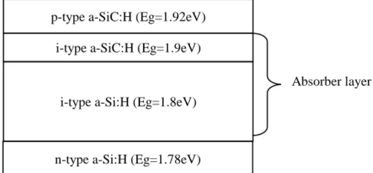
The structure as designed is shown in figure 1. The structure is composed of a glass window, a transparent conductor oxide (TCO) anode, a P-I-N junction and a Al cathode. The input set used in our simulation is reported in Table 1.
Fig. 1. Schematic view of a-Si:H single-junction solar cell.
TABLE I. PARAMETERS USED IN THE SIMULATION.
Parameters Structures layer
p-aSiC:H i-aSiC:H i-aSi:H n-aSi:H
Thickness [nm] 10 varied 570 12
Mobility gap [eV] 1.92 1.90 1.72 1.78 Electron mobility [cm2/Vs] 20 20 20 20 Hole mobility [cm2/Vs] 2 2 2 2 Effective DOS in CB [/cm3] 2x10 20 1x10²⁰ 1x10²⁰ 1x10²⁰ Effective DOS in VB [/cm3] 2x10 20 1x10²⁰ 1x10²⁰ 1x10²⁰
The basic solar cell performance parameters are the short circuit current density Jsc, the open circuit voltage Voc , the fill factor FF and the efficiency η. These parameters are briefly discussed below.
A. Short circuit current density Jsc
The flow of carriers into the external circuit constitutes a reverse electrical current density which under short circuit
i-type a-SiC:H (Eg=1.9eV) p-type a-SiC:H (Eg=1.92eV)
i-type a-Si:H (Eg=1.8eV)
n-type a-Si:H (Eg=1.78eV)
conditions (V = 0) is known as the short circuit current density Jsc. By convention, we take Jsc as a positive quantity, and describe the actual current density at short circuit as either +Jsc or -Jsc, depending on the current reference adopted.
B. Open circuit voltage Voc
The separation of charges sets up a forward potential difference between the two contacts of the solar cell, which under open circuit conditions (J = 0) is known as the open circuit voltage Voc.
C. Fill Factor FF
The fill factor is a measure of the “squareness” of the
J-V curve under illumination and is defined as the ratio:
OC SC m m V J V J FF (1)
where Jm and Vm are respectively the values of current density and voltage at the maximum power condition. Again, Jm is treated as a positive quantity; the actual current at maximum power then is ± Jm depending on the current
reference. D. Efficiency η
The efficiency of the cell is the power density delivered at the maximum power point as a fraction of the incident light power density Pinc
(02) The four quantities Jsc,
Voc, FF and η are the key performance characteristics of a
solar cell. All of them should be defined for particular illumination conditions. The standard test conditions (STC) or standard reporting conditions (SRC) for solar cells are the Air Mass 1.5 Global spectrum („AM1.5G‟), an incident power density of 1000 W/m2 and a cell or module temperature of 300°K.
E. J-V characteristics
The overall current voltage response of the solar cell, its current voltage characteristic, is the sum of the short circuit current and the dark current. The dark current can usually be approximated quite well by a slight adaptation of the ideal Shockley equation. The J-V characteristic is then described by:
(3)
J0: is the saturation current density, q the elementary charge, k Boltzmann‟s constant and T the absolute temperature.
Thus, the expected current density at reverse bias in the dark is -J0. In Eq. (4), n is called the diode quality factor, or the
diode ideality factor. J = 0 yields
(4)
In real cells, the J-V curve deviates from the ideal Eq. (4) by parasitic effects, which can be described by two resistances, one in series (Rs) and one in parallel (Rsh) with the cell.
Series resistance is due to the resistance of the cell material to current flow, especially through the front surface to the contacts. The parallel resistance can be due to a leakage current trough the cell (e.g. around the edges of the device). Thus when parasitic resistances are included the diode equation (4) becomes:
(5) The single junction p-i-n a-Si:H solar cell performances depends on the following factors:
Number of photons with energies higher than the band gap;
Absorption coefficients;
Properties of the layers, particularly the absorber i-layers.
Generally, the single junction a-Si:H cell uses p-type layers of a-SiC:H semiconductor deposited on n-type a-Si:H semiconductor, which is an intermediate intrinsic layer between p- and n-type layers. To improve the efficiency of this solar cell, the main attention should be paid mainly to obtaining a high short-circuit current Jsc by developing light traps as well as a higher open-circuit voltage Voc [6]. There are several ways to increase the performances of solar cells which the use of different alloys of a-Si in absorber layer, each of which uses a certain part of the spectrum of solar radiation for the production of electric current.
In a-Si:H p-i-n solar cell, the intrinsic layer can play a key role in improvement solar cell performances. The most important task in optimizing the i-layer is to understand the relation of its properties and deposition conditions, and the controllable range of the properties as a whole. The number of absorbed photons can be controlled by adjusting the gap width of each layer, the absorption coefficient of the material also depends on the characteristics of the material constituting each layer. Consequently, the current of each layer can be controlled by varying the layer thickness. For example, if the number of photons entered in each layer is the same, the layers with low coefficient of absorption must be thicker than the other, to absorb the same number of photons as the other layers, as well as produce the same number of electron-hole pairs. The optical and electrical properties of the a-Si:H intrinsic layer are of prime importance in the performance of a-Si solar cells. Recent studies have shown the following important facts concerning the relation between the absorber layer properties and solar cell performance and their improvements [7].
Another way to increase the efficiency of solar cells is the use of such layers, each of which uses a certain part of the spectrum of solar radiation for the production of electric current [10-12]. The strategies to increase the use of the light in the intrinsic layer are to reduce the optic losses in the non active regions of the cell and increasing the light confinement by redesign the intrinsic layer structure in using a-Si:H alloys like a-SiC:H and a-SiGe:H or µc-Si:H to have an intrinsic tandem, multi- or hetero-layer [11].
inc OC SC inc m m
P
FF
V
J
P
V
J
ln 1 0 J J q nkT V SC OC SC J nkT qV J J 0 exp 1
SC sh S S J A R A JR V nkT A JR V q J J 0 expIII. RESULT AND DISCUSSION
This paper attempts to show a solar cell simulation that is based on graded band-gap (intrinsic multilayer) in single junction. Modelling and analysis has been shown numerically that absorber multi-layer structure can enhance the efficiency of solar cell at the same thickness of single intrinsic layer. The optimization of the characteristics of intrinsic layer can improve significantly the solar cell parameters Voc, Jsc , FF, and efficiency.
In order to evaluate the effect of i-layer thickness on the solar cell performances, short-circuit current density (Jsc), open-circuit voltage (Voc), fill factor (FF) and conversion efficiency (η) are simulated as a function of i-layer thickness, seen fig 2.
Fig. 2. Photovoltaic parameters of Si:H solar cell as a function of a-SiC:H i-layer thickness, (a) Open circuit voltage, (b) short circuit current density, (c) Fill factor, (d) Efficiency.
The fill factor FF and open circuit voltatge Voc of the solar cell under AM1.5 illumination represented on fig.2 (a) initially increase until achieving its maximum value in the range 1-3nm and then slightly decreases with the increasing of the a-SiC:H i-layer thickness. However, the short circuit current density (Jsc) increase as a function of a-SiC:H i-layer thickness to reach 16.69mA/cm2 f or thickness from 2 to 10nm. As a result, the highest efficiency (Eff) can be achieved in the range 1-3nm of buffer layer thickness. On the other hand, a significant drop in efficiency in the range 3-10nm is due to the decline in VOC and rapid deterioration
of the FF when the thickness is over 5nm.
Fig. 3. Simulated current-voltage characteristics of the (p) a-SiC:H/(i)a-SiC:H/(i)a-Si:H/(n)a-Si:H structures.
In this paper, we verified that the best characteristics of p-i-n solar cells are when the value of the open-circuit voltage (Voc), short-circuit current density (Jsc), fill factor (FF), and efficiency (η) are 0.89 V, 16.69 mA/cm2, and 77.3%, respectively for grading band-gap a-SiC:H/a-Si:H/a-Si:H of 1.92eV, 1.9eV 1.8eV and 1.78eV, respectively. Thus, the graded bandgap was significantly performed compared with other studies of simple solar cell [2-4. After a numerical analysis of a single-junction a-Si:H solar cells and its optimizing, the best efficiency achieved is 11.52% that is the highest efficiency in comparison to a maximum value of the similar solar cell efficiency [11-12],.
IV. CONCLUSIONS
The optimized p-a-SiC:H/i-a-SiC:H-buffer/i-a-Si:H/n-a-Si:H single-junction solar cell has been designed numerically to investigate the design validation for higher efficiency. The simulation results demonstrate the effect of i-a-SiC:H layer into the absorber layer due to the variation of thickness thus the best efficiency achieved is 11.52% for grading bandgap a-Si:H solar cell. These results indicate that a-SiC:H intrinsic layer is a promising candidate for use as a top cell in tandem and multi junction solar cells.
REFERENCES
[1] Jae-Won Shin, Kwang-Mook Park, Jin-Eui Kim, And Sie-Young Choi, “The Properties of a-Si:H p-i-n Solar Cell by Intrinsic Layer‟s Thickness”. Mol. Cryst. Liq.Cryst.,Vol.551: pp.257–263, 2011. [2] Haruhisa Hashimoto, Shinya Tsuda, “Effects of the i-layer properties
and impurity on the performance of a-Si solar cells”. Solar Energy Materials and Solar Cells 34 (1994) 303-312.
[3] Peyman Jelodarian and Abdolnabi Kosarian, “Effect of p-Layer and i-Layer Properties on the Electrical Behaviour of Advanced
a-Si:H/a-0 5 10 15 0.870 0.875 0.880 0.885 0.890 Voc (V) Thickness (nm) Voc 0 5 10 15 16.64 16.66 16.68 16.70 Jsc (m A/cm 2 ) Thickness (nm) Jsc 0 5 10 15 76.0 76.5 77.0 77.5 FF (%) Thickness (nm) FF 0 5 10 15 11.2 11.3 11.4 11.5 Eff (%) Thickness (nm) Eff 0.0 0.2 0.4 0.6 0.8 1.0 -120 -100 -80 -60 -40 -20 0 20 J( mA /c m 2) V(V) Vco= 0.89V Jsc=16.69 mA/cm2 FF=77.30 % = 11.52 % (a) (b) (c) (d)
SiGe:H Thin Film Solar Cell from Numerical Modeling Prospect,” International Journal of Photoenergy Volume 2012,.
[4] Yutaka Hayashi, , Debin Li, Atsushi Ogura, and Yoshio Ohshita “ Role of i-aSi:H Layers in aSi:H/cSi Heterojunction Solar Cells,” IEEE journal of photovoltaics, vol. 3, no. 4, october 2013.
[5] Khikmat Kh. Muminov, Ashrafalsadat S. Mirkamali, “ Simulation of the Efficiency of a-SiC:H/a-Si:H Tandem Multilayer Solar Cells,”. [6] Hung-Jung Hsu, Cheng-Hang Hsu, and Chuang-Chuang Tsai, “ The
Effect of Bandgap Graded Absorber on the Performance of a-Si1– xGex:H Single-Junction Cells with �c-SiOx:H N-Type Layer,” International Journal of Photoenergy Volume 2013,.
[7] L. Ayat, A. F. Bouhdjar, AF. Meftah ., and N. Sengouga. “Numerical simulation of the effect of the free carrier motilities on light-soaked a-Si:Hp–i–n solar cell”. J. Semicond. 2015, 36(7)..
[8] Mingming Lia, et al , « Silicon content influence on structure and photoluminescence properties of carbon rich hydrogenated amorphous silicon carbide thin films”, Journal of Alloys and Compounds, Volume 753, 15 July 2018, Pages 320-328..
[9] Benslimane Hassane, Dennai Benmoussa, “Simulation of graded band gap p-i-n GaN/InN solar cell using AMPS-1D”, The 5th International
Conference on Electrical Engineering – Boumerdes (ICEE-B). October 29-31, 2017, Boumerdes, Algeria.
[10] Wilfried G.J.H.M. van Sark · Lars Korte Francesco Roca (Eds.), “Physics and Technology of Amorphous-Crystalline Heterostructure Silicon Solar Cells”. 2012 Springer-Verlag Berlin Heidelberg
[11] Seung Yeop Myong,a) Sang Soo Kim, and Koeng Su Lim. “ Improvement of pin-type amorphous silicon solar cell performance by employing double silicon-carbide p -layer structure ”. J. Appl. Phys., Vol. 95, No. 3, 1 February 2004/.
[12] T. Zimmermann, et al, « High-Rate Deposition of Intrinsic a-Si:H and μc-Si:H Layers for Thin-Film Silicon Solar Cells using a Dynamic Deposition Process”,Mater. Res. Soc. Symp. Proc. Vol. 1426 © 2012 Materials Research Society.
[13] Hiroyuki Fujiwaraa_ and Michio Kondo. “ Effects of a-Si:H layer thicknesses on the performance of a-Si:H/c-Si heterojunction solar cells ” Journal Of Applied Physics 101, 054516 _2007.
[14] Gourab Das · Sourav Mandal Sumita Mukhopadhyay Chandan Banerjee Asok K. Barua1. “ Effect of oxide based graded buffer and bottom n-layer on the performance of the single junction amorphous silicon solar cells, ” JMater Sci: Mater Electron.