Open
Archive TOULOUSE
Archive Ouverte (OATAO)
OATAO is an open access repository that collects the work of Toulouse researchers and
makes it freely available over the web where possible.
This is an author-deposited version published in : http://oatao.univ-toulouse.fr/
Eprints ID : 9311
To cite this version :
Trinsoutrot, Pierre and Rabot, Caroline and Vergnes, Hugues and
Delamoreanu, Alexandru and Zenasni, Aziz and Caussat, Brigitte
High quality graphene synthesized by atmospheric pressure CVD
on copper foil. (2013) In: 19th European Conference on Chemical
Vapor Deposition (EuroCVD19), 1- 6 Sept 2013, Varna, Bulgaria.
Any correspondance concerning this service should be sent to the repository
administrator: [email protected]
To link to this article : DOI:
10.1016/j.surfcoat.2013.06.050
URL : http://dx.doi.org/10.1016/j.surfcoat.2013.06.050
High quality graphene synthesized by atmospheric pressure CVD on
copper foil
Pierre Trinsoutrot
a, Caroline Rabot
b, Hugues Vergnes
a, Alexandru Delamoreanu
b,c,
Aziz Zenasni
b, Brigitte Caussat
a,⁎
aUniversité de Toulouse, Laboratoire de Génie Chimique, ENSIACET/INP Toulouse/UMR CNRS 5503, 4 allée Émile Monso, BP 44362, 31432 Toulouse Cedex 4, France bCEA, LETI, MINATEC Campus, 17 rue des Martyrs, 38054 Grenoble Cedex 9, France
cUJF-Grenoble 1/CNRS/CEA LTM, 17 rue des Martyrs, 38054 Grenoble Cedex 9, France
a b s t r a c t
Keywords: Graphene CVD Copper Methane Raman spectroscopyGraphene was synthesized at 1000 °C by Atmospheric Pressure Chemical Vapor Deposition on copper foil from methane diluted in argon and hydrogen. The influence of the main synthesis parameters was studied on 2 × 2 cm2foils in order to obtain continuous monolayer graphene without crystalline defect. The uniformity,
crystal quality and number of layers of graphene were analyzed by Raman spectroscopy and Scanning Electronic Microscopy. First, an increase of the annealing pre-treatment duration induced an increase of the average size of copper grains, leading to larger graphene flakes of higher crystallinity presenting a lower number of layers. Similar evolutions of graphene characteristics were observed when decreasing the methane concentration to 20 ppm, whereas an increase of run duration led to a loss of graphene quality and to a higher number of graphene layers, confirming that graphene formation is not self-limiting on copper. An optimum hydrogen/ methane ratio was found, quite different from other results of the literature, probably due to differences in the copper pre-treatment step. Finally, an optimized three step process was developed to form monolayer continuous graphene of high quality, successfully transposed to 7 × 7 cm2substrates after a reactor scale-up.
1. Introduction
Graphene is a single atomic layer of carbon atoms bonded in a hexag-onal lattice, exhibiting high mobility and optical transparency, in addi-tion to flexibility, robustness and environmental stability. Graphene attracts enormous interest thanks to this extraordinary combination of properties, in particular in the fields of optoelectronics and transparent conductors[1–3]. Graphene synthesis on copper by chemical vapor de-position (CVD) has become the favored approach to form high quality transferable graphene, due to the potential for large area, increasingly inexpensive, commercially viable production[4]. However, utilization of such graphene in many applications requires systematic optimization of the CVD processes for obtaining selective single or bilayer growth, as well as highly crystalline, large area domains[5]. Indeed, CVD processes have typically yielded polycrystalline graphene films composed of rela-tively small graphene grains (also called flakes). The higher density of grain boundaries degrades the physical and chemical properties of graphene[6]. Thus, it is desirable to prepare large single-crystal graphene to minimize the impact of defects found at grain boundaries. Similarly, good optical properties will be obtained by minimizing the number of graphene layers[7]. The CVD synthesis of graphene on Cu has long
been considered to be surface mediated and self-limiting due to the ex-tremely low carbon solubility in Cu, leading to the formation of monolay-er films[4]. However these last years, it has been shown that such self-limiting behavior only exists under specific conditions, in particular very low pressure and small amount of carbon precursor[8,9]. Atmo-spheric Pressure CVD (APCVD) would obviously be more suited to large-scale production than Low Pressure or Ultra High Vacuum CVD. Despite many efforts to understand the influences of the copper substrate characteristics and of the synthesis conditions on the graphene features, there are still many challenges to be solved to form large monolayer graphene domains of high crystalline quality on large surfaces.
In this framework, the present study concerns the synthesis of graphene by APCVD on copper foils from methane diluted in argon and hydrogen. We first investigate experimentally the influence of the copper surface crystalline state and of the main synthesis conditions on the graphene crystalline quality, number of layers and homogeneity on 2 × 2 cm2substrates. Then, optimized synthesis conditions are found
to form homogeneous mono and bi-layer graphene of high crystalline quality. Finally, after a reactor scale-up, the process is successfully reproduced on 7 × 7 cm2substrates.
2. Experimental
The CVD reactor consists in a horizontal tube in quartz of 1400 mm length and 50 mm inner diameter. A three zone furnace of 760 mm
⁎ Corresponding author. Tel.: +33 5 34 32 36 32; fax: +33 5 34 32 36 97. E-mail address:[email protected](B. Caussat).
length surrounds the reactor. The 25 μm-thick copper foils (99.999% Alfa Aesar, 2 × 2 cm2) were placed in the central isothermal zone of
the reactor, using a substrate holder which maintains them vertically during the process, as detailed below. They were heated to 1000 °C in a 20 sccm H2and 400 to 1200 sccm Ar flow and annealed for 1 to 3 h.
Then between 0.0125 and 0.05 sccm of methane, corresponding to methane concentrations between 10 and 120 ppm, were introduced into the reactor during 30 to 90 min, with the same Ar and H2flow
rates. The samples were then cooled to room temperature with an average rate of 16 °C/min under the same Ar/H2flow rates without
methane. Raman spectroscopy (confocal Raman microscope Labram — Horiba Yvon Jobin) with a laser excitation wavelength of 532 nm and optical microscopy were used to evaluate the thickness, crystalline quality and uniformity of graphene at room temperature. Each spec-trum was obtained by 5 acquisitions of 30 s accumulation time. Three to six analyses were systematically performed at various places on each sample. The morphology of graphene films was analyzed using Scanning Electron Microscopes (Jeol JSM 6700F and SEM Hitachi 5500). The copper crystal state was analyzed by X-Ray Diffraction (XRD, SIEMENS D5000).
3. Results and discussion
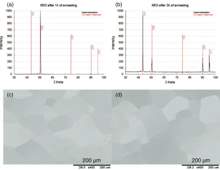
First, two pre-deposition annealing durations were studied, 1 h and 3 h. For some samples, the process was stopped just before the deposition step, and the copper surface was analyzed by XRD. As shown inFig. 1(a) and (b), after 1 h the Cu substrate mainly presents
oriented (100) grains, whereas after 3 h, (111), (100), (311) and (111) peaks appear. Similar polycrystalline orientations have also been found in other studies[3,10]. SEM views ofFig. 1(c) and (d) show that the average size of copper grains is about several hundreds of microns and tends to be higher after 3 h. This trend is confirmed by the FWHM (full width at half maximum) of the (100) peak which is thinner after 3 h, which means that longer annealing duration leads to a larger average size of grains.
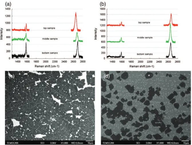
After annealing, the copper substrate was exposed to 120 ppm of methane for 30 min. As shown inFig. 2(a) and (b), graphene nuclei are smaller and more numerous after 1 h of annealing than after 3 h. This observation is in agreement with Wang et al.[11]and Han et al.[12]results, which have shown that longer annealing time sig-nificantly reduces graphene nucleation.
The corresponding Raman spectra are presented inFig. 2(c) and (d). The disorder-induced D-peak (~1345 cm− 1) intensity is clearly
lower after 3 h of annealing. Moreover, the average number of layers estimated from the 2D (~ 2689 cm− 1)/G (~ 1591 cm− 1) peak ratios, is
also lower after 3 h. Indeed, graphene is mostly 3–4 layers after 1 h and 1–2 layers after 3 h.
According to several authors, during annealing, the surface rough-ness and the number of defects of the copper substrate are decreased due to an enhanced crystal state, the level of volatile impurities and contaminants is reduced [11] and the surface oxide is eliminated thanks to the presence of hydrogen[13]. Therefore, the Cu active sites for graphene nucleation are reduced leading to less numerous and larger graphene domains. According to Vlassiouk et al.[3], the
(a)
(b)
(c)
(d)
200 µm
200 µm
crystallographic orientation of the Cu foil may affect the carbon pre-cursor dehydrogenation and adsorption, the generation of hydrogen atoms and the surface diffusion, all steps able to modify the number of graphene layers.
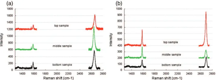
Then, the influence of methane concentration was studied for annealing durations of 3 h. Two samples were synthesized at 20 and 40 ppm of methane. Raman analyses are presented inFig. 3(a) and (b). A small peak before the G band is present on some spectra. We verified by specific Raman analyses on the copper substrate that it is due to the substrate and that it only appears when the Raman intensity of graphene peaks is low. Such variations of intensities are related to the crystalline orientation of the substrate[14]. In both cases, graphene presents few or no defects. This was also the case at 120 ppm of methane (Fig. 2(d)), meaning that for this range of oper-ating conditions, this absence of defects is mainly due to the Cu surface state induced by the 3 h annealing. Graphene synthesized at 20 ppm is strictly monolayer, whereas with 40 ppm of methane, the resulting graphene is mono or bilayers with multilayer spots. This result is in agreement with those found in the literature, since the maximum methane concentrations allowing the synthesis of mono-layer graphene vary from 5 ppm to 41 ppm[9]. According to Vlassiouk et al.[3], the highest concentration of activated carbon exists at the beginning of the process, when the open surface area of the catalyst is maximum. If the inlet CH4 concentration is not kept low enough,
multi-layer graphene is formed, which means that under APCVD condi-tions, graphene synthesis on copper is not always self-limiting, as also observed by other authors[8,15,16]. The mechanisms involved in the formation of multi-layer graphene on copper are not yet understood.
According to Li et al.[16], due to the weak carbon–copper interactions, ad-layers could form simultaneously and beneath the first layer by diffu-sion of carbon species between the catalytic substrate and the first layer.
Fig. 3(c) and (d) shows SEM views of the two samples. Obviously, a decrease of the methane concentration leads to a decrease of the nuclei density and to an increase of the nuclei average size. Wu et al.[9]also found that the amount of injected methane greatly influ-ences graphene nucleation and growth. They observed the same evo-lutions as ours. Luo et al.[17]also obtained high quality graphene using very low methane concentrations.
The hydrogen/methane ratio is also crucial in graphene synthesis. It is now well-known that hydrogen acts as an activator of surface-bound carbon and also as an etching agent controlling the size and morphology of graphene domains[18]. Losurdo et al.[19]reported no graphene synthesis without hydrogen and a degradation of graphene quality at too high H2concentration, thus confirming this dual role. It
is then necessary to find an optimal hydrogen/methane ratio. Here, two ratios were tested, 800 and 400 for 20 ppm of methane. The Raman spectra given inFig. 4clearly point out a decrease in graphene quality for the ratio of 400. The average number of layers is increased and a nonnegligible D-band is present. On the opposite, the ratio of 800 leads to a high quality monolayer graphene. In their study, Vlassiouk et al.[3]mentioned an optimal H2/CH4ratio of 300, but for
synthesis conditions involving different substrate pre-treatments and higher residence time of gas into the reactor.
The SEM analyses performed indicate that all the results obtained above correspond to discontinuous graphene (i.e. flakes). For photonic and optoelectronic applications, high quality continuous graphene is
necessary. In order to reach a full coverage, the deposition duration was then finally increased from 60 min to 90 min. Raman spectra are presented inFig. 5. This duration increase did not allow obtaining con-tinuous graphene and led to a loss of graphene quality. Indeed, bi and multilayers appear and the amount of defects is slightly higher. Wu et al.[9]and Wang et al.[11]observed an increase of the surface coverage without a marked evolution of the number of graphene layers, but for deposition durations not exceeding 60 min. The non-self-limiting
behavior of graphene synthesis for the tested conditions is then confirmed.
The difficulty to obtain a full coverage of the substrate with graphene of high quality has already been mentioned[9,16]. Wu et al.[9]have shown that if the methane concentration is too low, a complete cover-age would necessitate very long run durations. The most efficient way to obtain a continuous monolayer of graphene seems to use a several step process, first involving a very low methane concentration in order
Fig. 3. Raman spectra of graphene formed with (a) 40 ppm, (b) 20 ppm of methane — SEM views of graphene formed with (c) 40 ppm, (d) 20 ppm of methane.
to form strictly monolayer graphene flakes with low nucleation density. Then, methane concentration is progressively increased, to counter-balance the decrease of active copper area. The aim is to maintain a steady-state carbon ad-atom supply and to get complete monolayer graphene coverage with large grain size [9,16], thus ensuring good physical properties.
An optimized three step process was then developed. The methane concentrations used were 10 ppm for 1 h, 40 ppm for 1 h and 9500 ppm for the final step of 5 min. Raman spectra taken on 6 different points on the sample are given inFig. 6(a). They are all similar even if some small variations can be noticed on the 2D peak position. They can be attributed to differences in graphene stress which can vary according to the copper crystal orientation. These differences can lead to modifications of the 2D peak position over the sample without any change in the graphene layer number[20,21]. SEM views confirmed that the graphene film is homogeneous and continuous. Moreover, the graphene presents a high crystalline quality, as indicated by the very low D-band intensity. Only mono and bilayers (2D/G peak ratios > 1) were observed over the entire copper surface.
The process was then reproduced on a larger CVD reactor, 100 mm internal diameter, 760 mm length, using the same furnace. This reactor allows to treat Cu substrates of 7 × 7 cm2
. The gas flow
rates were increased to keep the same residence time of the gas phase. Similar Raman spectra (Fig. 6(b)) and SEM views were obtained, showing that an industrialization of the process could be considered.
4. Conclusion
The aim of the study was to develop an Atmospheric Pressure Chemical Vapor Deposition process for the synthesis of graphene with characteristics suitable for opto-electronics uses. A parametric study was conducted to understand the influence of each key param-eter on the crystal state, number of layers, density and size of nuclei and continuity of graphene. Based on these results, a three step pro-cess involving a progressive increase of methane concentration was developed. Graphene obtained by this process has a good crystalline quality and is mostly formed of continuous mono-bi-layers. A larger decrease of the methane concentration in the last step would probably allow the synthesis of strictly monolayer graphene film. Finally, the three-step process originally developed on 2 × 2 cm2copper foils has
been successfully reproduced on 7 × 7 cm2copper foils after a reactor scale-up. The analysis of the synthesized graphene performances in terms of transparency and electrical conductivity is in progress.
Fig. 5. Raman spectra for run durations of (a) 60 min, (b) 90 min at 20 ppm of methane.
Fig. 6. Raman spectra of graphene produced from an optimized three step process (a) on a 2 × 2 cm2
Cu foil, (b) on a 7 × 7 cm2
Acknowledgments
The work was supported by the FP7-NMP GRENADA European project. The authors acknowledge M. Molinier and E. Prevot from LGC/INP de Toulouse for technical support.
References
[1] J. Zhang, P.A. Hu, X. Wang, Z. Wang, Chem. Phys. Lett. 536 (2012) 123–128.
[2] Y.H. Zhang, Z.Y. Chen, B. Wang, Y.W. Wu, Z. Jin, X.Y. Liu, G.H. Yu, Mater. Lett. 96 (2013) 149–151.
[3] I. Vlassiouk, P. Fulvio, H. Meyer, N. Lavrik, S. Dai, P. Datskos, S. Smirnov, Carbon 54 (2013) 58–67.
[4] X.S. Li, W. Cai, J. An, S. Kim, J. Nah, D. Yang, R. Piner, A. Velamakanni, I. Jung, E. Tutuc, S.K. Banerjee, L. Colombo, R.S. Ruoff, Science 324 (2009) 1312–1314.
[5] K. Celebi, M.T. Cole, J.W. Choi, F. Wyczisk, P. Legagneux, N. Rupesinghe, J. Robertson, K.B.K. Teo, H.G. Park, Nano Lett. 13 (2013) 967–974.
[6] S. Chen, H. Ji, H. Chou, Q. Li, H. Li, J.W. Suk, R. Piner, L. Liao, W. Cai, R.S. Ruoff, Adv. Mater. 25 (2013) 2062–2065.
[7] X. Li, Y. Zhu, W. Cai, M. Borysiak, B. Han, D. Chen, R.D. Piner, L. Colombo, R.S. Ruoff, Nano Lett. 9 (2009) 4359–4363.
[8] S. Bhaviripudi, X. Jia, M.S. Dresselhaus, J. Kong, Nano Lett. 10 (2010) 4128–4133.
[9] W. Wu, Q. Yu, P. Peng, Z. Liu, J. Bao, S.S. Pei, Nanotechnology 23 (2012) 035603.
[10] J.D. Wood, S.W. Schmucker, A.S. Lyons, E. Pop, J.W. Lyding, Nano Lett. 11 (2011) 4547–4554.
[11] H. Wang, G. Wang, P. Bao, S. Yang, W. Zhu, X. Xie, W.J. Zhang, JACS 134 (2012) 3627-3630.
[12] G.H. Han, F. Günes, J.J. Bae, E.S. Kim, S.J. Chae, H.J. Shin, J.Y. Choi, D. Pribat, Y.H. Lee, Nano Lett. 11 (2011) 4144–4148.
[13] M.H. Yamukyan, K.V. Manukyan, S.L. Kharatyan, J. Alloys Compd. 473 (2009) 546–549.
[14] L.M. Malard, M.A. Pimenta, G. Dresselhaus, M.S. Dresselhaus, Phys. Rep. 473 (2009) 51–87.
[15] M. Kalbac, O. Frank, L. Kavan, Carbon 50 (2012) 3682–3687.
[16] Q. Li, H. Chou, J.H. Zhong, J.Y. Liu, A. Dolocan, J. Zhang, Y. Zhou, R.S. Ruoff, S. Chen, W. Cai, Nano Lett. 13 (2013) 486–490.
[17] Z. Luo, S. Kim, N. Kawamoto, A.M. Rappe, A.T. Charlie Johnson, ACS Nano 5 (2011) 9154–9160.
[18] I. Vlassiouk, M. Regmi, P. Fulvio, S. Dai, P. Datskos, G. Eres, ACS Nano 5 (2011) 6069–6076.
[19] M. Losurdo, M.M. Giangregorio, P. Capezzuto, G. Bruno, Phys. Chem. Chem. Phys. 13 (2011) 20836–20843.
[20] M. Mohr, J. Maultzsch, C. Thomsen, Phys. Rev. B 82 (2010) 201409–201410.
[21] T.M.G. Mohiuddin, A. Lombardo, R.R. Nair, A. Bonetti, G. Savini, R. Jalil, N. Bonini, D.M. Basko, C. Galiotis, N. Marzari, K.S. Novoselov, A.K. Geim, A.C. Ferrari, Phys. Rev. B 79 (2009) 205433–205442.